MC10EPT20, MC100EPT20 3.3V TTL/CMOS to Differential ... - Darlas
MC10EPT20, MC100EPT20 3.3V TTL/CMOS to Differential ... - Darlas
MC10EPT20, MC100EPT20 3.3V TTL/CMOS to Differential ... - Darlas

You also want an ePaper? Increase the reach of your titles
YUMPU automatically turns print PDFs into web optimized ePapers that Google loves.
The <strong>MC10EPT20</strong> is a 3.3 V <strong>TTL</strong>/<strong>CMOS</strong> <strong>to</strong> differential PECL<br />
transla<strong>to</strong>r. Because PECL (Positive ECL) levels are used, only +3.3 V<br />
and ground are required. The small outline 8–lead SOIC package and the<br />
single gate of the EPT20 makes it ideal for those applications where<br />
space, performance, and low power are at a premium.<br />
The 100 Series contains temperature compensation.<br />
• 390 ps Typical Propagation Delay<br />
• Maximum Frequency > 1 Ghz Typical<br />
• <strong>Differential</strong> 3.3 V PECL Outputs<br />
• PNP <strong>TTL</strong> Inputs for Minimal Loading<br />
• V CC Range of 3.0V <strong>to</strong> 3.6V<br />
• ESD Protection: >1.5 KV HBM, >200 V MM, >2 KV CDM<br />
• Q Output will default HIGH with inputs open<br />
• Meets or Exceeds JEDEC Spec EIA/JESD78 IC Latchup Test<br />
• Moisture Sensitivity Level 1, Indefinite Time Out of Drypack.<br />
For Additional Information, See Application Note AND8003/D<br />
• Flammability Rating: UL–94 code V–0 @ 1/8”,<br />
Oxygen Index 28 <strong>to</strong> 34<br />
• Transis<strong>to</strong>r Count = 150 devices<br />
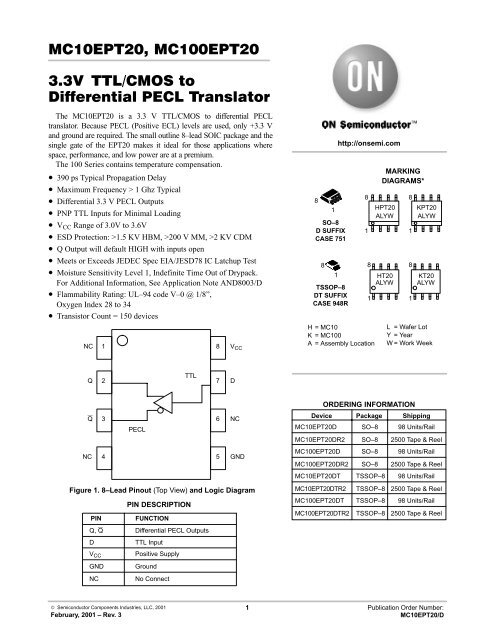
NC<br />
1<br />
8<br />
V CC<br />
8<br />
SO–8<br />
D SUFFIX<br />
CASE 751<br />
8<br />
1<br />
1<br />
TSSOP–8<br />
DT SUFFIX<br />
CASE 948R<br />
http://onsemi.com<br />
8<br />
1<br />
8<br />
1<br />
H = MC10<br />
K = MC100<br />
A = Assembly Location<br />
MARKING<br />
DIAGRAMS*<br />
HPT20<br />
ALYW<br />
HT20<br />
ALYW<br />
8<br />
KPT20<br />
ALYW<br />
1<br />
8<br />
1<br />
KT20<br />
ALYW<br />
L = Wafer Lot<br />
Y = Year<br />
W = Work Week<br />
Q<br />
2<br />
<strong>TTL</strong><br />
7<br />
D<br />
Q 3<br />
6 NC<br />
PECL<br />
NC 4 5 GND<br />
Figure 1. 8–Lead Pinout (Top View) and Logic Diagram<br />
PIN DESCRIPTION<br />
PIN<br />
FUNCTION<br />
Q, Q <strong>Differential</strong> PECL Outputs<br />
D<br />
<strong>TTL</strong> Input<br />
V CC<br />
Positive Supply<br />
GND Ground<br />
NC<br />
No Connect<br />
ORDERING INFORMATION<br />
Device Package Shipping<br />
<strong>MC10EPT20</strong>D SO–8 98 Units/Rail<br />
<strong>MC10EPT20</strong>DR2 SO–8 2500 Tape & Reel<br />
<strong>MC100EPT20</strong>D SO–8 98 Units/Rail<br />
<strong>MC100EPT20</strong>DR2 SO–8 2500 Tape & Reel<br />
<strong>MC10EPT20</strong>DT TSSOP–8 98 Units/Rail<br />
<strong>MC10EPT20</strong>DTR2 TSSOP–8 2500 Tape & Reel<br />
<strong>MC100EPT20</strong>DT TSSOP–8 98 Units/Rail<br />
<strong>MC100EPT20</strong>DTR2 TSSOP–8 2500 Tape & Reel<br />
© Semiconduc<strong>to</strong>r Components Industries, LLC, 2001<br />
February, 2001 – Rev. 3<br />
1 Publication Order Number:<br />
<strong>MC10EPT20</strong>/D
<strong>MC10EPT20</strong>, <strong>MC100EPT20</strong><br />
MAXIMUM RATINGS (Note 1.)<br />
Symbol Parameter Condition 1 Condition 2 Rating Units<br />
V CC Power Supply GND = 0 V 6 V<br />
V I Input Voltage GND = 0 V V I V CC 6 V<br />
I out Output Current Continuous<br />
Surge<br />
50<br />
100<br />
mA<br />
mA<br />
TA Operating Temperature Range –40 <strong>to</strong> +85 °C<br />
T stg S<strong>to</strong>rage Temperature Range –65 <strong>to</strong> +150 °C<br />
θ JA Thermal Resistance (Junction <strong>to</strong> Ambient) 0 LFPM<br />
500 LFPM<br />
8 SOIC<br />
8 SOIC<br />
190<br />
130<br />
°C/W<br />
°C/W<br />
θ JC Thermal Resistance (Junction <strong>to</strong> Case) std bd 8 SOIC 41 <strong>to</strong> 44 °C/W<br />
θ JA Thermal Resistance (Junction <strong>to</strong> Ambient) 0 LFPM<br />
500 LFPM<br />
8 TSSOP<br />
8 TSSOP<br />
185<br />
140<br />
°C/W<br />
°C/W<br />
θ JC Thermal Resistance (Junction <strong>to</strong> Case) std bd 8 TSSOP 41 <strong>to</strong> 44 °C/W<br />
T sol Wave Solder
<strong>MC10EPT20</strong>, <strong>MC100EPT20</strong><br />
AC CHARACTERISTICS V CC = 3.0 V <strong>to</strong> 3.6 V; GND = 0 V (Note 6.)<br />
–40°C 25°C 85°C<br />
Symbol Characteristic Min Typ Max Min Typ Max Min Typ Max Unit<br />
f max<br />
Maximum Frequency<br />
(See Figure 2. F max /JITTER)<br />
> 1 > 1 > 1 GHz<br />
t PLH ,<br />
t PHL<br />
Propagation Delay <strong>to</strong><br />
Output <strong>Differential</strong> 280 350 430 300 370 450 320 400 490<br />
ps<br />
t SKEW Device–<strong>to</strong>–Device Skew (Note 7.) 150 150 170 ps<br />
t JITTER<br />
Cycle–<strong>to</strong>–Cycle Jitter<br />
(See Figure 2. F max /JITTER)<br />
1 < 2 1 < 2 1 < 2 ps<br />
t r Output Rise/Fall Times Q, Q<br />
t f (20% – 80%)<br />
70 100 170 80 120 180 90 140 190 ps<br />
6. Measured using a 750 mV source, 50% duty cycle clock source. All loading with 50 ohms <strong>to</strong> V CC –2.0 V.<br />
7. Skew is measured between outputs under identical transitions.<br />
900<br />
9<br />
VOLTAGE (mV)<br />
800<br />
700<br />
600<br />
500<br />
400<br />
300<br />
200<br />
8<br />
7<br />
6<br />
5<br />
4<br />
3<br />
2<br />
ps (RMS)<br />
100<br />
1<br />
ÉÉÉÉ<br />
(JITTER)<br />
0<br />
0 200 400 600 800 1000 1200 1400 1600<br />
ÉÉÉÉ<br />
ÉÉÉÉ<br />
FREQUENCY (MHz)<br />
Figure 2. F max /Jitter<br />
http://onsemi.com<br />
3
<strong>MC10EPT20</strong>, <strong>MC100EPT20</strong><br />
Driver<br />
Device<br />
Q<br />
Qb<br />
D<br />
Db<br />
Receiver<br />
Device<br />
50 50 <br />
V TT<br />
V TT = V CC – 2.0 V<br />
Figure 3. Typical Termination for Output Driver and Device Evaluation<br />
(See Application Note AND8020 – Termination of ECL Logic Devices.)<br />
Resource Reference of Application Notes<br />
AN1404 – ECLinPS Circuit Performance at Non–Standard V IH Levels<br />
AN1405 – ECL Clock Distribution Techniques<br />
AN1406 – Designing with PECL (ECL at +5.0 V)<br />
AN1504 – Metastability and the ECLinPS Family<br />
AN1568 – Interfacing Between LVDS and ECL<br />
AN1650 – Using Wire–OR Ties in ECLinPS Designs<br />
AN1672 – The ECL Transla<strong>to</strong>r Guide<br />
AND8001 – Odd Number Counters Design<br />
AND8002 – Marking and Date Codes<br />
AND8009 – ECLinPS Plus Spice I/O Model Kit<br />
AND8020 – Termination of ECL Logic Devices<br />
http://onsemi.com<br />
4
<strong>MC10EPT20</strong>, <strong>MC100EPT20</strong><br />
PACKAGE DIMENSIONS<br />
–X–<br />
B<br />
–Y–<br />
–Z–<br />
H<br />
<br />
<br />
G<br />
A<br />
D<br />
<br />
<br />
S<br />
C<br />
<br />
<br />
<br />
<br />
SO–8<br />
D SUFFIX<br />
PLASTIC SOIC PACKAGE<br />
CASE 751–07<br />
ISSUE V<br />
<br />
<br />
<br />
N X 45<br />
M<br />
K<br />
J<br />
<br />
<br />
<br />
<br />
<br />
<br />
<br />
<br />
<br />
<br />
<br />
<br />
<br />
<br />
<br />
<br />
<br />
<br />
<br />
<br />
<br />
<br />
<br />
<br />
<br />
<br />
http://onsemi.com<br />
5
<strong>MC10EPT20</strong>, <strong>MC100EPT20</strong><br />
PACKAGE DIMENSIONS<br />
TSSOP–8<br />
DT SUFFIX<br />
CASE 948R–02<br />
ISSUE A<br />
<br />
<br />
L<br />
<br />
<br />
<br />
–T– <br />
<br />
<br />
2X L/2<br />
PIN 1<br />
IDENT<br />
<br />
C<br />
D<br />
8 5<br />
1<br />
8x<br />
A<br />
–V–<br />
K REF<br />
4<br />
<br />
G<br />
B<br />
–U–<br />
<br />
<br />
<br />
M<br />
F<br />
DETAIL E<br />
DETAIL E<br />
–W–<br />
<br />
<br />
<br />
<br />
<br />
<br />
<br />
<br />
<br />
<br />
<br />
<br />
<br />
<br />
<br />
<br />
<br />
<br />
<br />
<br />
<br />
<br />
<br />
<br />
<br />
<br />
<br />
http://onsemi.com<br />
6
<strong>MC10EPT20</strong>, <strong>MC100EPT20</strong><br />
Notes<br />
http://onsemi.com<br />
7
<strong>MC10EPT20</strong>, <strong>MC100EPT20</strong><br />
ON Semiconduc<strong>to</strong>r and are trademarks of Semiconduc<strong>to</strong>r Components Industries, LLC (SCILLC). SCILLC reserves the right <strong>to</strong> make changes<br />
without further notice <strong>to</strong> any products herein. SCILLC makes no warranty, representation or guarantee regarding the suitability of its products for any particular<br />
purpose, nor does SCILLC assume any liability arising out of the application or use of any product or circuit, and specifically disclaims any and all liability,<br />
including without limitation special, consequential or incidental damages. “Typical” parameters which may be provided in SCILLC data sheets and/or<br />
specifications can and do vary in different applications and actual performance may vary over time. All operating parameters, including “Typicals” must be<br />
validated for each cus<strong>to</strong>mer application by cus<strong>to</strong>mer’s technical experts. SCILLC does not convey any license under its patent rights nor the rights of others.<br />
SCILLC products are not designed, intended, or authorized for use as components in systems intended for surgical implant in<strong>to</strong> the body, or other applications<br />
intended <strong>to</strong> support or sustain life, or for any other application in which the failure of the SCILLC product could create a situation where personal injury or<br />
death may occur. Should Buyer purchase or use SCILLC products for any such unintended or unauthorized application, Buyer shall indemnify and hold<br />
SCILLC and its officers, employees, subsidiaries, affiliates, and distribu<strong>to</strong>rs harmless against all claims, costs, damages, and expenses, and reasonable<br />
at<strong>to</strong>rney fees arising out of, directly or indirectly, any claim of personal injury or death associated with such unintended or unauthorized use, even if such claim<br />
alleges that SCILLC was negligent regarding the design or manufacture of the part. SCILLC is an Equal Opportunity/Affirmative Action Employer.<br />
PUBLICATION ORDERING INFORMATION<br />
NORTH AMERICA Literature Fulfillment:<br />
Literature Distribution Center for ON Semiconduc<strong>to</strong>r<br />
P.O. Box 5163, Denver, Colorado 80217 USA<br />
Phone: 303–675–2175 or 800–344–3860 Toll Free USA/Canada<br />
Fax: 303–675–2176 or 800–344–3867 Toll Free USA/Canada<br />
Email: ONlit@hibbertco.com<br />
Fax Response Line: 303–675–2167 or 800–344–3810 Toll Free USA/Canada<br />
N. American Technical Support: 800–282–9855 Toll Free USA/Canada<br />
EUROPE: LDC for ON Semiconduc<strong>to</strong>r – European Support<br />
German Phone: (+1) 303–308–7140 (Mon–Fri 2:30pm <strong>to</strong> 7:00pm CET)<br />
Email: ONlit–german@hibbertco.com<br />
French Phone: (+1) 303–308–7141 (Mon–Fri 2:00pm <strong>to</strong> 7:00pm CET)<br />
Email: ONlit–french@hibbertco.com<br />
English Phone: (+1) 303–308–7142 (Mon–Fri 12:00pm <strong>to</strong> 5:00pm GMT)<br />
Email: ONlit@hibbertco.com<br />
EUROPEAN TOLL–FREE ACCESS*: 00–800–4422–3781<br />
*Available from Germany, France, Italy, UK, Ireland<br />
CENTRAL/SOUTH AMERICA:<br />
Spanish Phone: 303–308–7143 (Mon–Fri 8:00am <strong>to</strong> 5:00pm MST)<br />
Email: ONlit–spanish@hibbertco.com<br />
Toll–Free from Mexico: Dial 01–800–288–2872 for Access –<br />
then Dial 866–297–9322<br />
ASIA/PACIFIC: LDC for ON Semiconduc<strong>to</strong>r – Asia Support<br />
Phone: 303–675–2121 (Tue–Fri 9:00am <strong>to</strong> 1:00pm, Hong Kong Time)<br />
Toll Free from Hong Kong & Singapore:<br />
001–800–4422–3781<br />
Email: ONlit–asia@hibbertco.com<br />
JAPAN: ON Semiconduc<strong>to</strong>r, Japan Cus<strong>to</strong>mer Focus Center<br />
4–32–1 Nishi–Gotanda, Shinagawa–ku, Tokyo, Japan 141–0031<br />
Phone: 81–3–5740–2700<br />
Email: r14525@onsemi.com<br />
ON Semiconduc<strong>to</strong>r Website: http://onsemi.com<br />
For additional information, please contact your local<br />
Sales Representative.<br />
http://onsemi.com<br />
8<br />
<strong>MC10EPT20</strong>/D