BYV72EW series
BYV72EW series
BYV72EW series
- No tags were found...

Create successful ePaper yourself
Turn your PDF publications into a flip-book with our unique Google optimized e-Paper software.
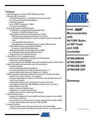
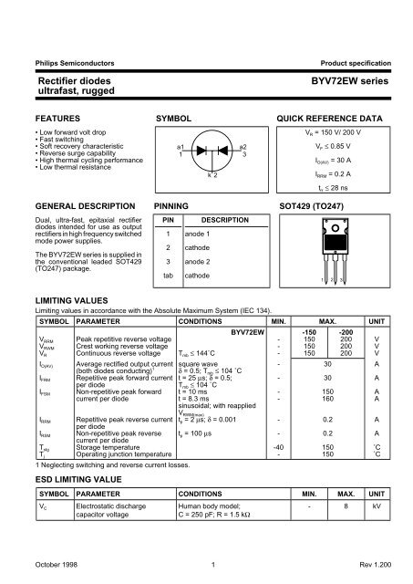
Philips Semiconductors<br />
Rectifier diodes<br />
ultrafast, rugged<br />
Product specification<br />
<strong>BYV72EW</strong> <strong>series</strong><br />
FEATURES SYMBOL QUICK REFERENCE DATA<br />
• Low forward volt drop<br />
• Fast switching<br />
• Soft recovery characteristic<br />
• Reverse surge capability<br />
• High thermal cycling performance<br />
• Low thermal resistance<br />
a1<br />
a2<br />
1 3<br />
k 2<br />
V R = 150 V/ 200 V<br />
V F ≤ 0.85 V<br />
I O(AV) = 30 A<br />
I RRM = 0.2 A<br />
t rr ≤ 28 ns<br />
GENERAL DESCRIPTION PINNING SOT429 (TO247)<br />
Dual, ultra-fast, epitaxial rectifier<br />
diodes intended for use as output<br />
PIN DESCRIPTION<br />
rectifiers in high frequency switched 1 anode 1<br />
mode power supplies.<br />
2 cathode<br />
The <strong>BYV72EW</strong> <strong>series</strong> is supplied in<br />
the conventional leaded SOT429<br />
(TO247) package.<br />
3 anode 2<br />
tab cathode<br />
1<br />
2 3<br />
LIMITING VALUES<br />
Limiting values in accordance with the Absolute Maximum System (IEC 134).<br />
SYMBOL PARAMETER CONDITIONS MIN. MAX. UNIT<br />
<strong>BYV72EW</strong> -150 -200<br />
V RRM Peak repetitive reverse voltage - 150 200 V<br />
V RWM Crest working reverse voltage - 150 200 V<br />
V R Continuous reverse voltage T mb ≤ 144˚C - 150 200 V<br />
I O(AV) Average rectified output current square wave - 30 A<br />
I FRM<br />
(both diodes conducting)<br />
Repetitive peak forward current<br />
δ = 0.5; T mb ≤ 104 ˚C<br />
t = 25 µs; δ = 0.5; - 30 A<br />
I FSM<br />
per diode<br />
Non-repetitive peak forward<br />
T mb ≤ 104 ˚C<br />
t = 10 ms - 150 A<br />
current per diode t = 8.3 ms - 160 A<br />
I RRM Repetitive peak reverse current<br />
RWM(max)<br />
t p = 2 µs; δ = 0.001<br />
sinusoidal; with reapplied<br />
V<br />
- 0.2 A<br />
per diode<br />
I RSM Non-repetitive peak reverse t p = 100 µs - 0.2 A<br />
current per diode<br />
T stg<br />
T j<br />
Storage temperature<br />
Operating junction temperature<br />
-40<br />
-<br />
150<br />
150<br />
˚C<br />
˚C<br />
1 Neglecting switching and reverse current losses.<br />
ESD LIMITING VALUE<br />
SYMBOL PARAMETER CONDITIONS MIN. MAX. UNIT<br />
V C Electrostatic discharge Human body model; - 8 kV<br />
capacitor voltage<br />
C = 250 pF; R = 1.5 kΩ<br />
October 1998 1 Rev 1.200
Philips Semiconductors<br />
Rectifier diodes<br />
ultrafast, rugged<br />
Product specification<br />
<strong>BYV72EW</strong> <strong>series</strong><br />
THERMAL RESISTANCES<br />
SYMBOL PARAMETER CONDITIONS MIN. TYP. MAX. UNIT<br />
R th j-mb Thermal resistance junction to per diode - - 2.4 K/W<br />
mounting base both diodes conducting - - 1.4 K/W<br />
R th j-a Thermal resistance junction to in free air - 45 - K/W<br />
ambient<br />
ELECTRICAL CHARACTERISTICS<br />
characteristics are per diode at T j = 25 ˚C unless otherwise stated<br />
SYMBOL PARAMETER CONDITIONS MIN. TYP. MAX. UNIT<br />
V F Forward voltage I F = 15 A; T j = 150˚C - 0.83 0.90 V<br />
I F = 15 A - 0.95 1.05 V<br />
I F = 30 A - 1.00 1.20 V<br />
I R Reverse current V R = V RWM ; T j = 100 ˚C - 0.5 1 mA<br />
V R = V RWM - 10 100 µA<br />
Q s Reverse recovery charge I F = 2 A; V R ≥ 30 V; -dI F /dt = 20 A/µs - 6 15 nC<br />
t rr1 Reverse recovery time I F = 1 A; V R ≥ 30 V; - 20 28 ns<br />
-dI F /dt = 100 A/µs<br />
t rr2 Reverse recovery time I F = 0.5 A to I R = 1 A; I rec = 0.25 A - 13 22 ns<br />
V fr Forward recovery voltage I F = 1 A; dI F /dt = 10 A/µs - 1 - V<br />
October 1998 2 Rev 1.200
Philips Semiconductors<br />
Rectifier diodes<br />
ultrafast, rugged<br />
Product specification<br />
<strong>BYV72EW</strong> <strong>series</strong><br />
I F<br />
I<br />
rrm<br />
t rr<br />
I = 1A<br />
dI<br />
F<br />
dt<br />
0.5A<br />
IF<br />
0A<br />
time<br />
I<br />
rec<br />
= 0.25A<br />
Q 100%<br />
s 10%<br />
IR<br />
trr2<br />
I<br />
R<br />
R<br />
Fig.1. Definition of t rr1 , Q s and I rrm<br />
Fig.4. Definition of t rr2<br />
time<br />
10<br />
V F<br />
V fr<br />
5<br />
Fig.2. Definition of V fr<br />
V F<br />
time<br />
I F<br />
0 5 10 15 20 25<br />
PF / W<br />
20<br />
Vo = 0.705 V<br />
Rs = 0.0097 Ohms<br />
BYV42<br />
Tmb(max) / C<br />
102<br />
D = 1.0<br />
15<br />
0.5<br />
114<br />
0.1<br />
0.2<br />
126<br />
I<br />
tp<br />
tp<br />
D =<br />
T<br />
138<br />
0<br />
IF(AV) / A<br />
Fig.5. Maximum forward dissipation P F = f(I F(AV) ) per<br />
diode; square current waveform where<br />
I F(AV) =I F(RMS) x √D.<br />
T<br />
t<br />
150<br />
Voltage Pulse Source<br />
R<br />
D.U.T.<br />
PF / W<br />
15<br />
10<br />
Vo = 0.705 V<br />
Rs = 0.0097 Ohms<br />
4<br />
BYV42<br />
2.8<br />
2.2<br />
Tmb(max) / C<br />
114<br />
a = 1.57<br />
1.9<br />
126<br />
Current<br />
shunt<br />
to ’scope<br />
5<br />
138<br />
Fig.3. Circuit schematic for t rr2<br />
0<br />
150<br />
0 5 10 15<br />
IF(AV) / A<br />
Fig.6. Maximum forward dissipation P F = f(I F(AV) ) per<br />
diode; sinusoidal current waveform where a = form<br />
factor = I F(RMS) / I F(AV) .<br />
October 1998 3 Rev 1.200
Philips Semiconductors<br />
Rectifier diodes<br />
ultrafast, rugged<br />
Product specification<br />
<strong>BYV72EW</strong> <strong>series</strong><br />
1000<br />
trr / ns<br />
100<br />
Qs / nC<br />
100<br />
IF=20A<br />
IF=20A<br />
10A<br />
5A<br />
2A<br />
1A<br />
IF=1A<br />
10<br />
10<br />
1<br />
1 10 100<br />
dIF/dt (A/us)<br />
Fig.7. Maximum t rr at T j = 25 ˚C; per diode<br />
1.0<br />
1.0 10 100<br />
-dIF/dt (A/us)<br />
Fig.10. Maximum Q s at T j = 25 ˚C; per diode<br />
10<br />
Irrm / A<br />
Transient thermal impedance, Zth j-mb (K/W)<br />
10<br />
IF=20A<br />
1<br />
1<br />
IF=1A<br />
0.1<br />
0.1<br />
0.01<br />
P<br />
D<br />
tp<br />
D =<br />
T<br />
tp<br />
0.01<br />
1 10 100<br />
-dIF/dt (A/us)<br />
Fig.8. Maximum I rrm at T j = 25 ˚C; per diode<br />
T<br />
t<br />
0.001<br />
1us 10us 100us 1ms 10ms 100ms 1s 10s<br />
pulse width, tp (s) BYV42E<br />
Fig.11. Transient thermal impedance; per diode;<br />
Z th j-mb = f(t p ).<br />
50<br />
40<br />
IF / A<br />
Tj = 150 C<br />
Tj = 25 C<br />
30<br />
20<br />
typ<br />
10<br />
0<br />
0<br />
max<br />
0.5 1.0<br />
1.5<br />
VF / V<br />
Fig.9. Typical and maximum forward characteristic<br />
I F = f(V F ); parameter T j<br />
October 1998 4 Rev 1.200
Philips Semiconductors<br />
Rectifier diodes<br />
ultrafast, rugged<br />
Product specification<br />
<strong>BYV72EW</strong> <strong>series</strong><br />
MECHANICAL DATA<br />
Dimensions in mm<br />
Net Mass: 5 g<br />
16 max<br />
5.3<br />
7.3<br />
1.8<br />
5.3 max<br />
o<br />
3.5<br />
max<br />
3.5<br />
21<br />
max<br />
15.5<br />
max<br />
seating<br />
plane<br />
2.5<br />
15.5<br />
min<br />
4.0<br />
max<br />
1<br />
2 3<br />
2.2 max<br />
3.2 max<br />
1.1<br />
0.4<br />
M<br />
0.9 max<br />
5.45<br />
5.45<br />
Notes<br />
1. Refer to mounting instructions for SOT429 envelope.<br />
2. Epoxy meets UL94 V0 at 1/8".<br />
Fig.12. SOT429 (TO247); pin 2 connected to mounting base.<br />
October 1998 5 Rev 1.200
Philips Semiconductors<br />
Rectifier diodes<br />
ultrafast, rugged<br />
Product specification<br />
<strong>BYV72EW</strong> <strong>series</strong><br />
DEFINITIONS<br />
Data sheet status<br />
Objective specification This data sheet contains target or goal specifications for product development.<br />
Preliminary specification This data sheet contains preliminary data; supplementary data may be published later.<br />
Product specification This data sheet contains final product specifications.<br />
Limiting values<br />
Limiting values are given in accordance with the Absolute Maximum Rating System (IEC 134). Stress above one<br />
or more of the limiting values may cause permanent damage to the device. These are stress ratings only and<br />
operation of the device at these or at any other conditions above those given in the Characteristics sections of<br />
this specification is not implied. Exposure to limiting values for extended periods may affect device reliability.<br />
Application information<br />
Where application information is given, it is advisory and does not form part of the specification.<br />
© Philips Electronics N.V. 1998<br />
All rights are reserved. Reproduction in whole or in part is prohibited without the prior written consent of the<br />
copyright owner.<br />
The information presented in this document does not form part of any quotation or contract, it is believed to be<br />
accurate and reliable and may be changed without notice. No liability will be accepted by the publisher for any<br />
consequence of its use. Publication thereof does not convey nor imply any license under patent or other<br />
industrial or intellectual property rights.<br />
LIFE SUPPORT APPLICATIONS<br />
These products are not designed for use in life support appliances, devices or systems where malfunction of these<br />
products can be reasonably expected to result in personal injury. Philips customers using or selling these products<br />
for use in such applications do so at their own risk and agree to fully indemnify Philips for any damages resulting<br />
from such improper use or sale.<br />
October 1998 6 Rev 1.200