TLP627,TLP627-2,TLP627-4 - Soemtron.org
TLP627,TLP627-2,TLP627-4 - Soemtron.org
TLP627,TLP627-2,TLP627-4 - Soemtron.org
- No tags were found...

Create successful ePaper yourself
Turn your PDF publications into a flip-book with our unique Google optimized e-Paper software.
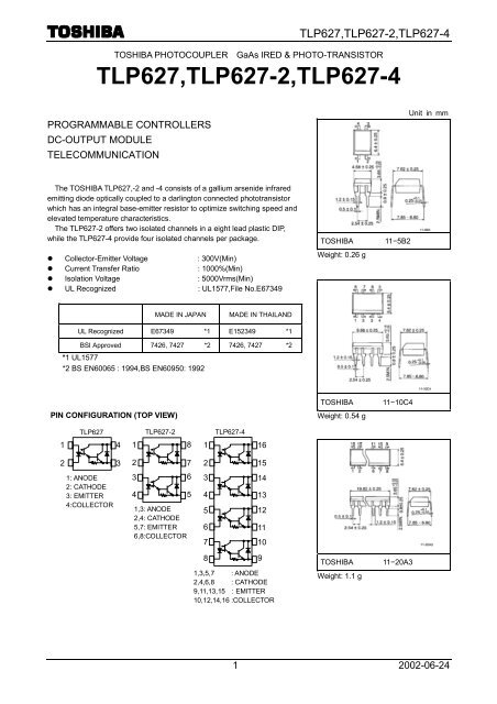
<strong>TLP627</strong>,<strong>TLP627</strong>-2,<strong>TLP627</strong>-4TOSHIBA PHOTOCOUPLER GaAs IRED & PHOTO-TRANSISTOR<strong>TLP627</strong>,<strong>TLP627</strong>-2,<strong>TLP627</strong>-4PROGRAMMABLE CONTROLLERSDC-OUTPUT MODULETELECOMMUNICATIONUnit in mmThe TOSHIBA <strong>TLP627</strong>,-2 and -4 consists of a gallium arsenide infraredemitting diode optically coupled to a darlington connected phototransistorwhich has an integral base-emitter resistor to optimize switching speed andelevated temperature characteristics.The <strong>TLP627</strong>-2 offers two isolated channels in a eight lead plastic DIP,while the <strong>TLP627</strong>-4 provide four isolated channels per package. Collector-Emitter Voltage Current Transfer Ratio Isolation Voltage UL Recognized: 300V(Min): 1000%(Min): 5000Vrms(Min): UL1577,File No.E67349TOSHIBAWeight: 0.26 g11−5B2MADE IN JAPANMADE IN THAILANDUL Recognized E67349 *1 E152349 *1BSI Approved 7426, 7427 *2 7426, 7427 *2*1 UL1577*2 BS EN60065 : 1994,BS EN60950: 1992PIN CONFIGURATION (TOP VIEW)TOSHIBAWeight: 0.54 g11−10C4<strong>TLP627</strong><strong>TLP627</strong>-2<strong>TLP627</strong>-414181162 3272151: ANODE2: CATHODE3: EMITTER4:COLLECTOR364 51,3: ANODE2,4: CATHODE5,7: EMITTER6,8:COLLECTOR345671413121110891,3,5,7 : ANODE2,4,6,8 : CATHODE9,11,13,15 : EMITTER10,12,14,16 :COLLECTORTOSHIBAWeight: 1.1 g11−20A31 2002-06-24
<strong>TLP627</strong>,<strong>TLP627</strong>-2,<strong>TLP627</strong>-4INDIVIDUAL ELECTRICAL CHARACTERISTICS (Ta=25°C)CHARACTERISTIC SYMBOL TEST CONDITION MIN. TYP. MAX. UNITForward Voltage V F I F = 10 mA 1.0 1.15 1.3 VLEDDETECTORReverse Current I R V R = 5 V — — 10 µACapacitance C T V = 0 , f=1MHz — 30 — pFCollector-EmitterBreakdown VoltageV (BR)CEO IC = 0.1mA 300 — — VEmitter-CollectorBreakdown VoltageCollector Dark CurrentV (BR)ECO IE = 0.1mA 0.3 — — VI CEOV CE = 200V — 10 200 nAV CE = 200V , Ta = 85°C — — 20 µACapacitance Collectorto EmitterC CE V=0 , f=1MHz — 10 — pFCOUPLED ELECTRICAL CHARACTERISTICS (Ta=25°C)CHARACTERISTIC SYMBOL TEST CONDITION MIN. TYP. MAX. UNITCurrent Transfer Ratio I C/I F I F=1mA , V CE=1V 1000 4000 — %Saturated CTR I C/I F(sat) I F=10mA , V CE=1V 500 — — %Collector-EmitterSaturation VoltageV CE(sat)I C=10mA , I F=1mA — — 1.0I C=100mA , I F=10mA 0.3 — 1.2VISOLATION ELECTRICAL CHARACTERISTICS (Ta=25°C)CHARACTERISTIC SYMBOL TEST CONDITION MIN. TYP. MAX. UNITCapacitance Input to Output C S V S=0 , f=1MHz — 0.8 — pFIsolation Resistance R S V S=500V , R.H.≤60% 510 10 10 14 — ΩIsolation VoltageBVsAC, 1minute 5000 — —AC, 1second, in oil — 10000 —VrmsDC, 1 minute, in oil — 10000 — Vdc3 2002-06-24
<strong>TLP627</strong>,<strong>TLP627</strong>-2,<strong>TLP627</strong>-4SWITCHING CHARACTERISTICS (Ta=25°C)CHARACTERISTIC SYMBOL TEST CONDITION MIN. TYP. MAX. UNITRise Time tr — 40 —Fall Time tfV CC=10VI C=10mA— 15 —Turn-on Time tonR L=1009— 50 —Turn-off Timetoff— 15 —Turn-on Time tON — 5 —Strage Time tsR L=1809 (Fig.1)V CC=10V , I F=16mA— 40 —Turn-off TimetOFF— 80 —µsFig.1 SWITCHING TIME TEST CIRCUITIFRLVCCVCEIFVCEts9VVCC1VtONtOFF4 2002-06-24
<strong>TLP627</strong>,<strong>TLP627</strong>-2,<strong>TLP627</strong>-45 2002-06-24
<strong>TLP627</strong>,<strong>TLP627</strong>-2,<strong>TLP627</strong>-46 2002-06-24
<strong>TLP627</strong>,<strong>TLP627</strong>-2,<strong>TLP627</strong>-47 2002-06-24
<strong>TLP627</strong>,<strong>TLP627</strong>-2,<strong>TLP627</strong>-4RESTRICTIONS ON PRODUCT USE000707EBC TOSHIBA is continually working to improve the quality and reliability of its products. Nevertheless, semiconductordevices in general can malfunction or fail due to their inherent electrical sensitivity and vulnerability to physicalstress. It is the responsibility of the buyer, when utilizing TOSHIBA products, to comply with the standards ofsafety in making a safe design for the entire system, and to avoid situations in which a malfunction or failure ofsuch TOSHIBA products could cause loss of human life, bodily injury or damage to property.In developing your designs, please ensure that TOSHIBA products are used within specified operating ranges asset forth in the most recent TOSHIBA products specifications. Also, please keep in mind the precautions andconditions set forth in the “Handling Guide for Semiconductor Devices,” or “TOSHIBA Semiconductor ReliabilityHandbook” etc.. The TOSHIBA products listed in this document are intended for usage in general electronics applications(computer, personal equipment, office equipment, measuring equipment, industrial robotics, domestic appliances,etc.). These TOSHIBA products are neither intended nor warranted for usage in equipment that requiresextraordinarily high quality and/or reliability or a malfunction or failure of which may cause loss of human life orbodily injury (“Unintended Usage”). Unintended Usage include atomic energy control instruments, airplane orspaceship instruments, transportation instruments, traffic signal instruments, combustion control instruments,medical instruments, all types of safety devices, etc.. Unintended Usage of TOSHIBA products listed in thisdocument shall be made at the customer’s own risk. Gallium arsenide (GaAs) is a substance used in the products described in this document. GaAs dust and fumesare toxic. Do not break, cut or pulverize the product, or use chemicals to dissolve them. When disposing of theproducts, follow the appropriate regulations. Do not dispose of the products with other industrial waste or withdomestic garbage. The products described in this document are subject to the foreign exchange and foreign trade laws. The information contained herein is presented only as a guide for the applications of our products. Noresponsibility is assumed by TOSHIBA CORPORATION for any infringements of intellectual property or otherrights of the third parties which may result from its use. No license is granted by implication or otherwise underany intellectual property or other rights of TOSHIBA CORPORATION or others. The information contained herein is subject to change without notice.8 2002-06-24