5420/DM5420/DM7420 Dual 4-Input NAND Gates
5420/DM5420/DM7420 Dual 4-Input NAND Gates
5420/DM5420/DM7420 Dual 4-Input NAND Gates

Create successful ePaper yourself
Turn your PDF publications into a flip-book with our unique Google optimized e-Paper software.
<strong>5420</strong>DM<strong>5420</strong><strong>DM7420</strong><br />
<strong>Dual</strong> 4-<strong>Input</strong> <strong>NAND</strong> <strong>Gates</strong><br />
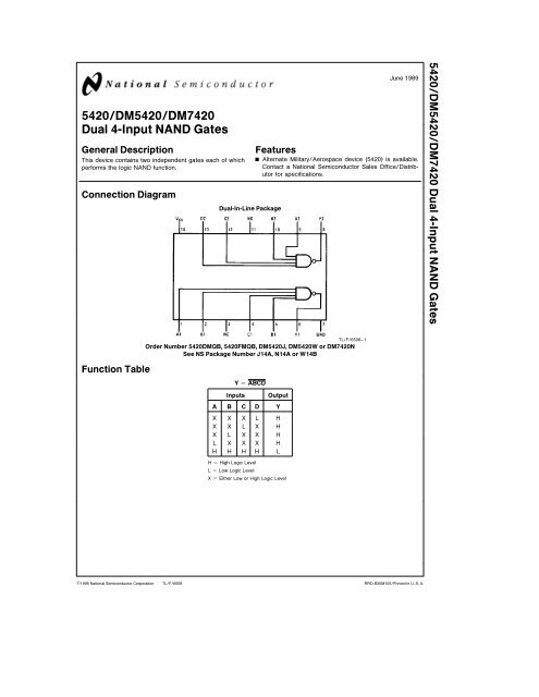
General Description<br />
This device contains two independent gates each of which<br />
performs the logic <strong>NAND</strong> function<br />
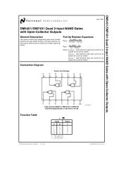
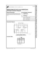
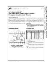
Connection Diagram<br />
Features<br />
Y<br />
<strong>Dual</strong>-In-Line Package<br />
June 1989<br />
Alternate MilitaryAerospace device (<strong>5420</strong>) is available<br />
Contact a National Semiconductor Sales OfficeDistributor<br />
for specifications<br />
<strong>5420</strong>DM<strong>5420</strong><strong>DM7420</strong> <strong>Dual</strong> 4-<strong>Input</strong> <strong>NAND</strong> <strong>Gates</strong><br />
Function Table<br />
TLF6506–1<br />
Order Number <strong>5420</strong>DMQB <strong>5420</strong>FMQB DM<strong>5420</strong>J DM<strong>5420</strong>W or <strong>DM7420</strong>N<br />
See NS Package Number J14A N14A or W14B<br />
Y e ABCD<br />
<strong>Input</strong>s<br />
Output<br />
A B C D Y<br />
X X X L H<br />
X X L X H<br />
X L X X H<br />
L X X X H<br />
H H H H L<br />
H e High Logic Level<br />
L e Low Logic Level<br />
X e Either Low or High Logic Level<br />
C1995 National Semiconductor Corporation<br />
TLF6506<br />
RRD-B30M105Printed in U S A
Absolute Maximum Ratings (Note)<br />
If MilitaryAerospace specified devices are required<br />
please contact the National Semiconductor Sales<br />
OfficeDistributors for availability and specifications<br />
Supply Voltage<br />
7V<br />
<strong>Input</strong> Voltage<br />
55V<br />
Operating Free Air Temperature Range<br />
DM54 and 54<br />
b55Ctoa125C<br />
DM74<br />
0Ctoa70C<br />
Storage Temperature Range<br />
b65Ctoa150C<br />
Recommended Operating Conditions<br />
Symbol<br />
Parameter<br />
Note The ‘‘Absolute Maximum Ratings’’ are those values<br />
beyond which the safety of the device cannot be guaranteed<br />
The device should not be operated at these limits The<br />
parametric values defined in the ‘‘Electrical Characteristics’’<br />
table are not guaranteed at the absolute maximum ratings<br />
The ‘‘Recommended Operating Conditions’’ table will define<br />
the conditions for actual device operation<br />
DM5402<br />
DM7402<br />
Min Nom Max Min Nom Max<br />
V CC Supply Voltage 45 5 55 475 5 525 V<br />
V IH High Level <strong>Input</strong> Voltage 2 2 V<br />
V IL Low Level <strong>Input</strong> Voltage 08 08 V<br />
I OH High Level Output Current b04 b04 mA<br />
I OL Low Level Output Current 16 16 mA<br />
T A Free Air Operating Temperature b55 125 0 70 C<br />
Electrical Characteristics over recommended operating free air temperature range (unless otherwise noted)<br />
Symbol Parameter Conditions Min<br />
Typ<br />
(Note 1)<br />
V I <strong>Input</strong> Clamp Voltage V CC e Min I I eb12 mA b15 V<br />
V OH High Level Output V CC e Min I OH e Max<br />
Voltage<br />
V IL e Max<br />
V OL Low Level Output V CC e Min I OL e Max<br />
Voltage<br />
V IH e Min<br />
I I <strong>Input</strong> Current Max V CC e Max V I e 55V<br />
<strong>Input</strong> Voltage<br />
Max<br />
Units<br />
Units<br />
24 34 V<br />
02 04 V<br />
1 mA<br />
I IH High Level <strong>Input</strong> Current V CC e Max V I e 24V 40 mA<br />
I IL Low Level <strong>Input</strong> Current V CC e Max V I e 04V b16 mA<br />
I OS Short Circuit V CC e Max DM54 b20 b55<br />
Output Current (Note 2)<br />
DM74 b18 b55<br />
I CCH Supply Current with V CC e Max<br />
Outputs High<br />
I CCL Supply Current with V CC e Max<br />
Outputs Low<br />
mA<br />
2 4 mA<br />
6 11 mA<br />
Switching Characteristics at V CC e 5V and T A e 25C (See Section 1 for Test Waveforms and Output Load)<br />
Symbol Parameter Conditions Min Max Units<br />
t PLH Propagation Delay Time C L e 15 pF<br />
Low to High Level Output<br />
R L e 400X<br />
22 ns<br />
t PHL<br />
Propagation Delay Time<br />
High to Low Level Output<br />
15 ns<br />
Note 1 All typicals are at V CC e 5V T A e 25C<br />
Note 2 Not more than one output should be shorted at a time<br />
2
Physical Dimensions inches (millimeters)<br />
14-Lead Ceramic <strong>Dual</strong>-In-Line Package (J)<br />
Order Number <strong>5420</strong>DMQB or DM<strong>5420</strong>J<br />
NS Package Number J14A<br />
14-Lead Molded <strong>Dual</strong>-In-Line Package (N)<br />
Order Number <strong>DM7420</strong>N<br />
NS Package Number N14A<br />
3
<strong>5420</strong>DM<strong>5420</strong><strong>DM7420</strong> <strong>Dual</strong> 4-<strong>Input</strong> <strong>NAND</strong> <strong>Gates</strong><br />
Physical Dimensions inches (millimeters) (Continued)<br />
14-Lead Ceramic Flat Package (W)<br />
Order Number <strong>5420</strong>FMQB or DM<strong>5420</strong>W<br />
NS Package Number W14B<br />
LIFE SUPPORT POLICY<br />
NATIONAL’S PRODUCTS ARE NOT AUTHORIZED FOR USE AS CRITICAL COMPONENTS IN LIFE SUPPORT<br />
DEVICES OR SYSTEMS WITHOUT THE EXPRESS WRITTEN APPROVAL OF THE PRESIDENT OF NATIONAL<br />
SEMICONDUCTOR CORPORATION As used herein<br />
1 Life support devices or systems are devices or 2 A critical component is any component of a life<br />
systems which (a) are intended for surgical implant support device or system whose failure to perform can<br />
into the body or (b) support or sustain life and whose be reasonably expected to cause the failure of the life<br />
failure to perform when properly used in accordance support device or system or to affect its safety or<br />
with instructions for use provided in the labeling can effectiveness<br />
be reasonably expected to result in a significant injury<br />
to the user<br />
National Semiconductor National Semiconductor National Semiconductor National Semiconductor<br />
Corporation Europe Hong Kong Ltd Japan Ltd<br />
1111 West Bardin Road Fax (a49) 0-180-530 85 86 13th Floor Straight Block Tel 81-043-299-2309<br />
Arlington TX 76017 Email cnjwge tevm2nsccom Ocean Centre 5 Canton Rd Fax 81-043-299-2408<br />
Tel 1(800) 272-9959 Deutsch Tel (a49) 0-180-530 85 85 Tsimshatsui Kowloon<br />
Fax 1(800) 737-7018 English Tel (a49) 0-180-532 78 32 Hong Kong<br />
Franais Tel (a49) 0-180-532 93 58 Tel (852) 2737-1600<br />
Italiano Tel (a49) 0-180-534 16 80 Fax (852) 2736-9960<br />
National does not assume any responsibility for use of any circuitry described no circuit patent licenses are implied and National reserves the right at any time without notice to change said circuitry and specifications