AN17820B - diagramas.diagram...
AN17820B - diagramas.diagram...
AN17820B - diagramas.diagram...

You also want an ePaper? Increase the reach of your titles
YUMPU automatically turns print PDFs into web optimized ePapers that Google loves.
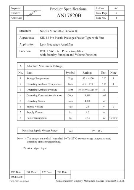
Prepared<br />
Checked<br />
Approved<br />
Tentative<br />
Product Specifications<br />
<strong>AN17820B</strong><br />
Ref No.<br />
Total Page<br />
Page No.<br />
A-1<br />
9<br />
1<br />
Structure<br />
Appearance<br />
Application<br />
Function<br />
Silicon Monolithic Bipolar IC<br />
SIL-12 Pin Plastic Package (Power Type with Fin)<br />
Low Frequency Amplifier<br />
BTL 7.5W x 2ch Power Amplifier<br />
with Standby Function and Volume Function<br />
A<br />
Absolute Maximum Ratings<br />
No.<br />
Item<br />
Symbol<br />
Ratings<br />
Unit<br />
Note<br />
1<br />
Storage Temperature<br />
Tstg<br />
-55 ~ +150<br />
° C<br />
1<br />
2<br />
Operating Ambient Temperature<br />
Topr<br />
-25 ~ +70<br />
° C<br />
1<br />
3<br />
Operating Ambient Pressure<br />
Popr<br />
1.013x10 5 ±0.61x10 5<br />
Pa<br />
4<br />
Operating Constant Acceleration<br />
Gopr<br />
9,810<br />
m/s 2<br />
5<br />
Operating Shock<br />
Sopr<br />
4,900<br />
m/s 2<br />
6<br />
Supply Voltage<br />
Vcc<br />
24<br />
V<br />
2<br />
7<br />
Supply Current<br />
Icc<br />
4.0<br />
A<br />
8<br />
Power Dissipation<br />
P D<br />
37.5<br />
W<br />
Ta=70°C<br />
Operating Supply Voltage Range Vcc 5V ~ 18V<br />
Note 1)<br />
2)<br />
The temperature of all items shall be Ta=25°C except storage temperature and<br />
operating ambient temperature.<br />
At no signal input.<br />
Eff. Date Eff. Date Eff. Date Eff. Date<br />
09-JUL-2001<br />
Semiconductor Company, Matsushita Electric Industrial Co., Ltd.<br />
FMSC-PSDA-002-01 Rev.1
Prepared<br />
Checked<br />
Approved<br />
Tentative<br />
Product Specifications<br />
<strong>AN17820B</strong><br />
Ref No.<br />
Total Page<br />
Page No.<br />
B-1<br />
9<br />
2<br />
B<br />
No Item<br />
1<br />
Electrical Characteristics<br />
Quiescent Circuit<br />
Current<br />
Symbol Test<br />
Circuit<br />
ICQ<br />
1<br />
(Unless otherwise specified, the ambient temperature is 25°C±2°C,<br />
Vcc=12V, frequency=1kHz and RL=8Ω.)<br />
Conditions<br />
Vin=0V, Vol=0V<br />
min<br />
-<br />
Limits<br />
typ max<br />
45<br />
100<br />
Unit<br />
mA<br />
Note<br />
2<br />
Standby Current<br />
ISTB<br />
1<br />
Vin=0V, Vol=0V<br />
-<br />
1<br />
10<br />
µA<br />
3<br />
Output Noise<br />
Voltage<br />
VNO<br />
1<br />
Rg=10kΩ, Vol=0V<br />
-<br />
0.2<br />
0.6<br />
mVrms<br />
1<br />
4<br />
Voltage Gain<br />
GV<br />
1<br />
Po=1.0W, Vol=1.25V<br />
38<br />
40<br />
42<br />
dB<br />
5<br />
Total Harmonic<br />
Distortion<br />
THD<br />
1<br />
Po=1.0W, Vol=1.25V<br />
-<br />
0.10<br />
0.5<br />
%<br />
6<br />
Maximum Power<br />
Output 1<br />
PO1<br />
1<br />
THD=10%, Vol=1.25V<br />
6.0<br />
7.5<br />
-<br />
W<br />
7<br />
Maximum Power<br />
Output 2<br />
PO2<br />
1<br />
Vcc=15V<br />
THD=10%, Vol=1.25V<br />
10.0<br />
12.5<br />
-<br />
W<br />
8<br />
Ripple Rejection<br />
Ratio<br />
RR<br />
1<br />
Rg=10kΩ, Vol=0V<br />
Vr=1Vrms, fr=120Hz<br />
30<br />
50<br />
-<br />
dB<br />
1<br />
9<br />
Output Offset<br />
Voltage<br />
Voff<br />
1<br />
Rg=10kΩ, Vol=0V<br />
-350<br />
0<br />
350<br />
mV<br />
10<br />
Volume<br />
Attenuation Ratio<br />
Att<br />
1<br />
Po=1.0W, Vol=0V<br />
70<br />
80<br />
-<br />
dB<br />
1<br />
11<br />
Channel Balance 1<br />
CB1<br />
1<br />
Po=1.0W, Vol=1.25V<br />
-1<br />
0<br />
1<br />
dB<br />
12<br />
Channel Balance 2<br />
CB2<br />
1<br />
Po=1.0W, Vol=0.6V<br />
-2<br />
0<br />
2<br />
dB<br />
13<br />
Middle Voltage<br />
Gain<br />
GVm<br />
1<br />
Po=1.0W, Vol=0.6V<br />
26.5<br />
29.5<br />
32.5<br />
dB<br />
14<br />
Channel Crosstalk<br />
CT<br />
1<br />
Po=1.0W, Vol=1.25V<br />
40<br />
55<br />
-<br />
dB<br />
Note 1) For this measurement, use the BPF = 15Hz ~ 30kHz (12dB/OCT).<br />
Eff. Date Eff. Date Eff. Date Eff. Date<br />
09-JUL-2001<br />
Semiconductor Company, Matsushita Electric Industrial Co., Ltd.<br />
FMSC-PSDA-002-01 Rev.1
Prepared<br />
Checked<br />
Approved<br />
Tentative<br />
Product Specifications<br />
<strong>AN17820B</strong><br />
Ref No.<br />
Total Page<br />
Page No.<br />
B-2<br />
9<br />
3<br />
B<br />
No Item<br />
1<br />
Electrical Characteristics<br />
Standby pin<br />
current<br />
Symbol Test<br />
Circuit<br />
ISTB2<br />
(Unless otherwise specified, the ambient temperature is 25°C±2°C,<br />
Vcc=12V, frequency=1kHz and RL=8Ω.)<br />
1<br />
Conditions<br />
min<br />
Vin=0V, VSTB=3V -<br />
Limits<br />
typ max<br />
-<br />
25<br />
Unit<br />
µA<br />
Note<br />
2<br />
Volume pin<br />
current<br />
IVOL<br />
1<br />
Vin=0V, Vol=0V<br />
-12<br />
-<br />
-<br />
µA<br />
3<br />
Input Impedance Zi 1 Vin=±0.3VDC<br />
24<br />
30<br />
36<br />
kΩ<br />
Note)<br />
The above characteristics are reference values determined for IC design, but not guaranteed<br />
values for shipping inspection. If problems were to occur, counter measures will be<br />
sincerely discussed.<br />
Eff. Date Eff. Date Eff. Date Eff. Date<br />
09-JUL-2001<br />
Semiconductor Company, Matsushita Electric Industrial Co., Ltd.<br />
FMSC-PSDA-002-01 Rev.1
Prepared<br />
Checked<br />
Approved<br />
Tentative<br />
Product Specifications<br />
<strong>AN17820B</strong><br />
Ref No.<br />
Total Page<br />
Page No.<br />
C-1<br />
9<br />
4<br />
(Description of test circuit and test method)<br />
Test Circuit 1<br />
<strong>AN17820B</strong><br />
1 2 3 4 5 6 7 8<br />
+<br />
470µ + +<br />
+<br />
1.0µ<br />
10µ 270k<br />
OUT1<br />
8Ω<br />
68k<br />
10k<br />
1.0µ<br />
10k<br />
9 10<br />
11<br />
OUT2<br />
8Ω<br />
12<br />
Vcc<br />
5V<br />
Vin1<br />
Vin2<br />
1.25V<br />
0V<br />
Stand-by<br />
0V<br />
Volume<br />
Note) If the standby pin is open or 0V, the IC is on standby state.<br />
The IC is in the state of volume minimum if the Volume pin is ground.<br />
The IC is in the state of volume maximum if the Volume pin is open.<br />
Eff. Date Eff. Date Eff. Date Eff. Date<br />
09-JUL-2001<br />
Semiconductor Company, Matsushita Electric Industrial Co., Ltd.<br />
FMSC-PSDA-002-01 Rev.1
_<br />
+<br />
_<br />
+<br />
Prepared<br />
Checked<br />
Approved<br />
Tentative<br />
Product Specifications<br />
<strong>AN17820B</strong><br />
Ref No.<br />
Total Page<br />
Page No.<br />
D-1<br />
9<br />
5<br />
Circuit Function Block Diagram<br />
+ _ _<br />
+<br />
1 2 3 4 5 6 7 8<br />
Vcc<br />
Output<br />
GND<br />
Input<br />
GND<br />
9 10 11 12<br />
Output<br />
GND<br />
Pin Descriptions<br />
Pin No.<br />
1<br />
2<br />
3<br />
4<br />
5<br />
6<br />
Description<br />
Vcc<br />
Ch.1 Output (+)<br />
GND (Ch.1 Output)<br />
Ch.1 Output (-)<br />
Standby<br />
Ch.1 Input<br />
Pin No. Description<br />
7 GND (Input)<br />
8 Ch.2 Input<br />
9 Volume<br />
10 Ch.2 Output (-)<br />
11 GND (Ch.2 Output)<br />
12 Ch.2 Output (+)<br />
Eff. Date Eff. Date Eff. Date Eff. Date<br />
09-JUL-2001<br />
FMSC-PSDA-002-01 Rev.1<br />
Semiconductor Company, Matsushita Electric Industrial Co., Ltd.
Prepared<br />
Checked<br />
Approved<br />
Tentative<br />
Product Specifications<br />
<strong>AN17820B</strong><br />
Ref No.<br />
Total Page<br />
Page No.<br />
E<br />
9<br />
6<br />
Package Name<br />
FP-12S<br />
Unit : mm<br />
∅ 3.6<br />
6.4 ± 0.3<br />
7.7 ± 0.3 7.8 ± 0.3<br />
29.96 ± 0.3<br />
0.6<br />
28.0 ± 0.3<br />
20.0±0.1<br />
R1.8<br />
1 12<br />
2.54<br />
1.2 ± 0.1<br />
0.25 +0.1<br />
-0.05<br />
3.5 ± 0.3<br />
0.6 ± 0.1<br />
29.6 ± 0.3<br />
Company<br />
insignia<br />
Name<br />
of item<br />
Date<br />
Code<br />
Eff. Date Eff. Date Eff. Date Eff. Date<br />
09-JUL-2001<br />
Semiconductor Company, Matsushita Electric Industrial Co., Ltd.<br />
FMSC-PSDA-002-01 Rev.1
Prepared<br />
Checked<br />
Approved<br />
Tentative<br />
Product Specifications<br />
<strong>AN17820B</strong><br />
Ref No.<br />
Total Page<br />
Page No.<br />
F-1<br />
9<br />
7<br />
(Structure Description)<br />
Chip surface passivation<br />
SiN,<br />
PSG,<br />
Others ( )<br />
1<br />
Lead frame material<br />
Fe group,<br />
Cu group,<br />
Others ( )<br />
2 , 6<br />
Inner lead surface process<br />
Ag plating,<br />
Au plating,<br />
Others ( )<br />
2<br />
Outer lead surface process<br />
Solder plating,<br />
Solder dip,<br />
Others ( )<br />
6<br />
Chip mounting method<br />
Ag paste,<br />
Au-Si alloy, Solder,<br />
Others ( )<br />
3<br />
Wire bonding method<br />
Thermalsonic bonding,<br />
Others ( )<br />
4<br />
Wire material, Diameter<br />
Au,<br />
Diameter 38 µm<br />
Others ( )<br />
4<br />
Mold material<br />
Epoxy,<br />
Others ( )<br />
5<br />
Molding method<br />
Transfer mold,<br />
Multiplunger mold,<br />
Others ( )<br />
5<br />
Fin material<br />
Cu Group<br />
Others ( )<br />
7<br />
Package FP-12S<br />
1<br />
5<br />
6<br />
4<br />
3<br />
2<br />
Eff. Date Eff. Date Eff. Date Eff. Date<br />
09-JUL-2001<br />
Semiconductor Company, Matsushita Electric Industrial Co., Ltd.<br />
FMSC-PSDA-002-01 Rev.1
Prepared<br />
Checked<br />
Approved<br />
Tentative<br />
Product Specifications<br />
<strong>AN17820B</strong><br />
Ref No.<br />
Total Page<br />
Page No.<br />
G-1<br />
9<br />
8<br />
PD - Ta Curves<br />
80<br />
(1) Tc = Ta, 62.5W ( θj-c = 2 °C/W )<br />
(2) 20.83W ( θf = 4.0 °C/W )<br />
2<br />
With a 100cm X 3mm Al heat sink (black colour coated)<br />
2<br />
or a 200cm X 2mm Al heat sink (not lacquered)<br />
(3) 15.63W ( θf = 6.0 °C/W )<br />
2<br />
With a 100cm X 2mm Al heat sink (not lacquered)<br />
(4) 3.0W at Ta = 25°C ( θj-a = 42 °C/W )<br />
Without heat sink<br />
70<br />
62.5W<br />
Power Dissipation PD ( W )<br />
60<br />
50<br />
40<br />
30<br />
(1)<br />
20<br />
20.8W<br />
15.6W<br />
(2)<br />
(3)<br />
10<br />
0<br />
3.0W (4)<br />
0 25 50 75 100 125 150<br />
Ambient Temperature Ta (°C )<br />
Eff. Date Eff. Date Eff. Date Eff. Date<br />
09-JUL-2001<br />
Semiconductor Company, Matsushita Electric Industrial Co., Ltd.<br />
FMSC-PSDA-002-01 Rev.1
Prepared<br />
Checked<br />
Approved<br />
Tentative<br />
Product Specifications<br />
<strong>AN17820B</strong><br />
Ref No.<br />
Total Page<br />
Page No.<br />
G<br />
9<br />
9<br />
(Precautions for use)<br />
1) Make sure that the IC is free of any pin short-circuiting, ground short, and load<br />
short-circuiting.<br />
2) Ground the radiation fin so that there will be no difference in electric potential<br />
between the radiation fin and ground.<br />
3) The thermal protection circuit operates at a Tj of approximately 150°C. The thermal<br />
protection circuit is reset automatically when the temperature drops.<br />
4) Make sure that the heat radiation design is effective enough if the Vcc is<br />
comparatively high or the IC operates high output power.<br />
5) Connect only ground pin for signal sources to the signal GND pin of the amplifier<br />
on the previous stage.<br />
Eff. Date Eff. Date Eff. Date Eff. Date<br />
09-JUL-2001<br />
Semiconductor Company, Matsushita Electric Industrial Co., Ltd.<br />
FMSC-PSDA-002-01 Rev.1