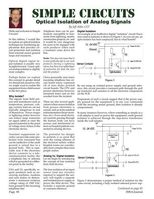
Simple Circuits - Optical Isolation of Analog Signals - IMSA
Simple Circuits - Optical Isolation of Analog Signals - IMSA
Simple Circuits - Optical Isolation of Analog Signals - IMSA

You also want an ePaper? Increase the reach of your titles
YUMPU automatically turns print PDFs into web optimized ePapers that Google loves.
Hello and welcome to <strong>Simple</strong><br />
<strong>Circuits</strong>!<br />
In this edition, I would like<br />
to explore an optical isolation<br />
technique for monitoring applications<br />
that provides circuit<br />
protection and isolation<br />
from external sensor ground<br />
loops and transients.<br />
<strong>Optical</strong> digital signal input<br />
isolation is usually very<br />
straight forward. Linear optical<br />
analog isolation is slightly<br />
more complex.<br />
<strong>Simple</strong> <strong>Circuits</strong><br />
<strong>Optical</strong> <strong>Isolation</strong> <strong>of</strong> <strong>Analog</strong> <strong>Signals</strong><br />
Telephone lines can be particularly<br />
susceptible to transients<br />
from lightning, nearby<br />
construction projects, etc. and<br />
it would be very dangerous<br />
for users to be engaged with<br />
such products when such<br />
a transient came down the<br />
line.<br />
Note: This does not mean that it<br />
is now perfectly safe to use such<br />
products during a lightning<br />
storm, but there is an added layer<br />
<strong>of</strong> protection for both the user<br />
and the product.<br />
By Jeff Alder, CET<br />
Digital <strong>Isolation</strong><br />
An example <strong>of</strong> an ineffective digital “isolation” circuit I have<br />
seen used in industry is shown in Figure 1. As you can see, an<br />
opto-isolator has been employed, but to what benefit<br />
Perhaps before we explore<br />
this concept in greater detail<br />
we should ask ourselves why<br />
we might want to isolate the<br />
equipment from a field sensor<br />
in the first place.<br />
Why Isolate<br />
The signals from field sensors<br />
and transducers such as<br />
temperature, pressure, voltage,<br />
current, load, etc. are not<br />
typically dangerous in and<br />
<strong>of</strong> themselves. Power surges<br />
or lightning strikes however<br />
can induce large transients<br />
on signal cables or raise the<br />
ground potential to the point<br />
<strong>of</strong> voltage stress failure in the<br />
electronic device.<br />
Transient suppression circuitry<br />
can provide some protection<br />
from transients but<br />
can be ineffective if the earth<br />
ground is raised due to a<br />
ground fault. This is especially<br />
true if the electronic<br />
device connects to a telecommunication<br />
facility like<br />
a telephone line or antenna<br />
which is grounded at a different<br />
point in the facility.<br />
I have personally seen many<br />
incoming telephone line circuit<br />
board traces vaporized<br />
<strong>of</strong>f <strong>of</strong> auto dialer printed<br />
circuit boards. The CPU and<br />
process electronics however,<br />
remained intact and no fire<br />
resulted from the incident.<br />
There are also several applications<br />
where sensor isolation<br />
from process electronics is<br />
crucial, such as in bio-medical<br />
instrumentation (heart monitors,<br />
etc.). Even small electrical<br />
currents passing through<br />
the human body can have<br />
serious and detrimental effects<br />
on hospital patients connected<br />
to sensing devices.<br />
The potential for danger<br />
to patients is so great that<br />
even the wiring schemes <strong>of</strong><br />
the electrical outlets within<br />
hospital rooms are considerably<br />
more complex than most<br />
people realize.<br />
<strong>Analog</strong> Vs. Digital <strong>Isolation</strong><br />
Let me begin by introducing<br />
the concept <strong>of</strong> true isolation<br />
from field devices.<br />
Figure 1<br />
By not using an isolated power supply and ground reference,<br />
this circuit provides a transient path through the pull<br />
up resistor(s) and common to all the electronic components<br />
on the PCB.<br />
Proponents <strong>of</strong> such a circuit suggest that if the power supply<br />
ground for the equipment is in any way commoned<br />
with the incoming sensor ground, then isolation is already<br />
compromised.<br />
In many instances however, where something as simple as a<br />
wall adapter is used to power the equipment, earth ground<br />
isolation is achieved through the step-down transformer<br />
inside the wall adapter.<br />
CSA and UL specifically require<br />
products such as answering<br />
machines, modems<br />
and auto dialers to demonstrate<br />
a minimum isolation<br />
voltage rating <strong>of</strong> 1500 VAC<br />
from ground to the incoming<br />
telephone line.<br />
Page 44<br />
The true isolation <strong>of</strong> an input<br />
sensor (and any circuitry<br />
required to support the sensor),<br />
will require a separate<br />
Figure 2<br />
and isolated power supply to Figure 2 demonstrates a proper method <strong>of</strong> isolation for the<br />
power the field device. This same circuit, including a fully isolated onboard power supincludes<br />
a separate ground<br />
or common reference. Continued on page 45<br />
<strong>IMSA</strong> Journal
<strong>Simple</strong> <strong>Circuits</strong> . . . Continued from page 44<br />
ply. The added power supply<br />
drives up the cost to build<br />
the circuit, but the protection<br />
is there, and incoming<br />
transients will not damage<br />
internal circuitry, providing<br />
the associated breakdown<br />
voltages <strong>of</strong> the power supply<br />
and opto-isolator are not<br />
exceeded.<br />
Although digital isolation is<br />
typically straightforward, analog<br />
signal isolation requires<br />
extra consideration if we<br />
are to accurately reproduce<br />
incoming signal levels.<br />
<strong>Analog</strong> <strong>Isolation</strong><br />
There are several techniques<br />
which can be implemented<br />
for the isolation <strong>of</strong> analog<br />
signals, and their usefulness<br />
depends on the application.<br />
One technique employs a<br />
front end analog to digital<br />
convertor with a serial interface.<br />
The sensor and A/D converter<br />
would be driven from<br />
the isolated power supply,<br />
with the digitized signal then<br />
serially streamed through a<br />
standard optocoupler to the<br />
CPU for processing.<br />
The drawback to such a technique<br />
comes from the fact<br />
that many analog signals are<br />
used for real time feedback<br />
control <strong>of</strong> external processes.<br />
These applications require<br />
a high speed or large bandwidth<br />
to ensure that feedback<br />
is not unduly delayed.<br />
When the incoming signal is<br />
required to function in such<br />
a capacity, the delays <strong>of</strong> the<br />
conversion time <strong>of</strong> the A/D,<br />
in addition to the streaming<br />
time <strong>of</strong> the serialized data are<br />
prohibitive.<br />
An Alternate <strong>Analog</strong><br />
<strong>Isolation</strong> Strategy<br />
The LOC110, manufactured<br />
by Clare (An IXYS Company),<br />
provides an excellent<br />
method to isolate and<br />
reproduce incoming analog<br />
signals, while minimizing<br />
delays when used in control<br />
applications.<br />
It is essentially an optocoupler<br />
in which two matched<br />
output phototransistors are<br />
driven by the same optical<br />
infrared LED.<br />
(Note: The LOC110 provides<br />
3750 volts <strong>of</strong> isolation and<br />
will operate down to -40C.)<br />
The LOC110 can be applied<br />
using two circuit configurations:<br />
1) A high bandwidth, lower<br />
linearity mode (Photoconductive<br />
Mode)<br />
2) A lower bandwidth,<br />
high linearity mode<br />
(Photovoltaic Mode)<br />
Photoconductive Mode<br />
In order to drive the input<br />
diode <strong>of</strong> the LOC110, application<br />
notes (AN-107),<br />
published by Clare, indicate<br />
that drive currents <strong>of</strong> 10mA<br />
to 15mA are desirable.<br />
In order to achieve<br />
this level <strong>of</strong> drive current,<br />
an input buffer<br />
op amp, which also<br />
functions as part <strong>of</strong> a<br />
negative feedback and<br />
linearization drive circuit,<br />
is employed.<br />
The Claire application<br />
note takes the reader<br />
through a mathematically<br />
derived process<br />
in which 3 types <strong>of</strong><br />
gain are taken into<br />
consideration when<br />
applying the circuit.<br />
1) Servo Gain (K1)<br />
– Servo Gain is a<br />
constant which<br />
is determined<br />
by the values <strong>of</strong><br />
the input diode<br />
current limiting<br />
resistor and<br />
the feedback resistor<br />
from the<br />
servo photodiode<br />
feedback<br />
output. (K1=I1/<br />
IF – Please see<br />
Figure 3)<br />
2) Forward Gain<br />
(K2) – Forward<br />
Gain is used to derive the transfer gain <strong>of</strong> the circuit –<br />
please see Transfer Gain.<br />
3) Transfer Gain – The Transfer Gain is important because<br />
it dictates the actual amplification gain <strong>of</strong> the entire<br />
circuit.<br />
Figure 3 <strong>Isolation</strong> Amplifier<br />
(Photoconductive Operation)<br />
In summary, the application note demonstrates the desired<br />
drive characteristics for the input diode and that the Ratio<br />
<strong>of</strong> R2 to R1 defines the gain <strong>of</strong> the entire signal conditioning<br />
circuit. This makes the device very straightforward to implement<br />
into applications.<br />
Photovoltaic Mode<br />
In the photovoltaic mode, a different control feedback configuration<br />
is used for the input buffer amplifier.<br />
In this instance, the output phototransistors function as current<br />
generators.<br />
Continued on page 46<br />
July/August 2012 Page 45
<strong>Simple</strong> <strong>Circuits</strong> . . . Continued from page 45<br />
The servo feedback control phototransistor is essentially<br />
placed across the two inputs <strong>of</strong> the input buffer op amp.<br />
This keeps the phototransistor at a 0V bias, as photogenerators<br />
display some voltage dependence on linearity, and the objective<br />
is to eliminate this issue, thereby improving linearity.<br />
As can be seen in Figure 4, the input amplifier is operating as<br />
an inverting amplifier. The incoming voltage is fed through a<br />
resistor into the negative input <strong>of</strong> the op amp. It is also applied<br />
to the collector <strong>of</strong> the feedback phototransistor.<br />
Figure 4 <strong>Isolation</strong> amplifier (Photovoltaic Operation)<br />
The output <strong>of</strong> the inverting input amplifier, sinks current<br />
through the input diode <strong>of</strong> the optocoupler, whose anode is<br />
pulled up to VCC through a current limiting resistor.<br />
As the input signal is increased, the inverting op amp begins<br />
to sink greater current through the input diode, which in turn<br />
drives the feedback phototransistor into higher conduction.<br />
The photocurrent through the servo control output transistor<br />
is linearly proportional to the input signal.<br />
As the feedback phototransistor conducts it bleeds <strong>of</strong>f current<br />
from the inverting input <strong>of</strong> the op amp, keeping it at 0 volts,<br />
thereby lowering the input signal to the op amp, providing<br />
the negative feedback control.<br />
The output photodiode drives an inverting amplifier, which<br />
inverts and amplifies the already linearized output signal<br />
such that it is properly polarized, and tracks the input signal<br />
as current flows away from the inverting input, into the collector<br />
<strong>of</strong> the output phototransistor.<br />
You will note that I have not attempted to review the math<br />
involved in the preceeding circuit analyses, only the operation<br />
<strong>of</strong> the circuits themselves. This is because Clare has produced<br />
an excellent application note (AN-107). Not only is the<br />
math very simple and straightforward, but it is thoroughly<br />
covered in the App note, which is available for download <strong>of</strong>f<br />
the internet.<br />
Six ranges <strong>of</strong> transfer gain are available for purchase for the<br />
LOC110. Even with factory pre-sorting, small amounts <strong>of</strong><br />
circuit calibration will still likely be required.<br />
Calibration can be accomplished by trimming the amplification<br />
gain resistors <strong>of</strong> the circuit.<br />
Additional Applications:<br />
I have not had the opportunity to cover many applications <strong>of</strong><br />
the LOC110 within the scope <strong>of</strong> this article. The LOC110 can<br />
also be used for modem DAA (Data Access Arrangement)<br />
circuits, where the device can replace the cumbersome isolation<br />
transformer <strong>of</strong> years past.<br />
The LOC110 can also be used in switch mode power supply<br />
designs, cardiac monitoring, isolating voltage to current converters,<br />
and RTD temperature measuring circuits, etc.<br />
You will find LOC11x series devices for sale on the internet<br />
for under $2.00 USD, and they also come with two completely<br />
independent opto-couplers in the same package (LOC21x<br />
series).<br />
An assortment <strong>of</strong> external amplifiers can be used with the<br />
LOC110 including the LM358, LM201, LM1558 and LMC6484.<br />
For high precision/accuracy applications, the AD824 has also<br />
been used. http://www.analog.com/static/imported-files/<br />
data_sheets/AD824.pdf<br />
Conclusion<br />
I would like to thank David Hickle, President <strong>of</strong> Xtel International<br />
for his assistance in the writing <strong>of</strong> this article and<br />
Clare for permission to use graphics (Figures 3 and 4) from<br />
the LOC110 App Note, AN-107.<br />
The LOC series <strong>of</strong> opto-isolators provide low cost, small form<br />
factor, and superior performance over traditional transformer<br />
interface designs, and are readily available from several suppliers.<br />
As always, I have tried to be as accurate as possible within<br />
the scope <strong>of</strong> my column, however, there are several aspects to<br />
this device which I have not had the opportunity to review.<br />
Please read the entire data sheet and application note before<br />
implementing this component into a design.<br />
Until next time,<br />
Take care out there!<br />
Repeatability and Circuit Calibration<br />
Any time a manufacturer produces an electronic component,<br />
they strive for specification consistency from part to part. This<br />
is not always easy to achieve, especially with components<br />
such as opto-isolators, where even the smallest physical<br />
difference can lead to varying performance charactaristics<br />
within a circuit.<br />
In order to compensate for differences in the LOC110, Clare<br />
actually tests and pre-sorts the LOC110 into batches, reflecting<br />
different transfer gain characteristics from various production<br />
runs.<br />
Page 46<br />
<strong>IMSA</strong> Journal