Simple Circuits - Optical Isolation of Analog Signals - IMSA
Simple Circuits - Optical Isolation of Analog Signals - IMSA
Simple Circuits - Optical Isolation of Analog Signals - IMSA

You also want an ePaper? Increase the reach of your titles
YUMPU automatically turns print PDFs into web optimized ePapers that Google loves.
<strong>Simple</strong> <strong>Circuits</strong> . . . Continued from page 44<br />
ply. The added power supply<br />
drives up the cost to build<br />
the circuit, but the protection<br />
is there, and incoming<br />
transients will not damage<br />
internal circuitry, providing<br />
the associated breakdown<br />
voltages <strong>of</strong> the power supply<br />
and opto-isolator are not<br />
exceeded.<br />
Although digital isolation is<br />
typically straightforward, analog<br />
signal isolation requires<br />
extra consideration if we<br />
are to accurately reproduce<br />
incoming signal levels.<br />
<strong>Analog</strong> <strong>Isolation</strong><br />
There are several techniques<br />
which can be implemented<br />
for the isolation <strong>of</strong> analog<br />
signals, and their usefulness<br />
depends on the application.<br />
One technique employs a<br />
front end analog to digital<br />
convertor with a serial interface.<br />
The sensor and A/D converter<br />
would be driven from<br />
the isolated power supply,<br />
with the digitized signal then<br />
serially streamed through a<br />
standard optocoupler to the<br />
CPU for processing.<br />
The drawback to such a technique<br />
comes from the fact<br />
that many analog signals are<br />
used for real time feedback<br />
control <strong>of</strong> external processes.<br />
These applications require<br />
a high speed or large bandwidth<br />
to ensure that feedback<br />
is not unduly delayed.<br />
When the incoming signal is<br />
required to function in such<br />
a capacity, the delays <strong>of</strong> the<br />
conversion time <strong>of</strong> the A/D,<br />
in addition to the streaming<br />
time <strong>of</strong> the serialized data are<br />
prohibitive.<br />
An Alternate <strong>Analog</strong><br />
<strong>Isolation</strong> Strategy<br />
The LOC110, manufactured<br />
by Clare (An IXYS Company),<br />
provides an excellent<br />
method to isolate and<br />
reproduce incoming analog<br />
signals, while minimizing<br />
delays when used in control<br />
applications.<br />
It is essentially an optocoupler<br />
in which two matched<br />
output phototransistors are<br />
driven by the same optical<br />
infrared LED.<br />
(Note: The LOC110 provides<br />
3750 volts <strong>of</strong> isolation and<br />
will operate down to -40C.)<br />
The LOC110 can be applied<br />
using two circuit configurations:<br />
1) A high bandwidth, lower<br />
linearity mode (Photoconductive<br />
Mode)<br />
2) A lower bandwidth,<br />
high linearity mode<br />
(Photovoltaic Mode)<br />
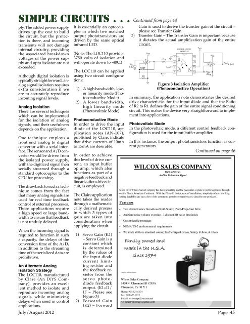
Photoconductive Mode<br />
In order to drive the input<br />
diode <strong>of</strong> the LOC110, application<br />
notes (AN-107),<br />
published by Clare, indicate<br />
that drive currents <strong>of</strong> 10mA<br />
to 15mA are desirable.<br />
In order to achieve<br />
this level <strong>of</strong> drive current,<br />
an input buffer<br />
op amp, which also<br />
functions as part <strong>of</strong> a<br />
negative feedback and<br />
linearization drive circuit,<br />
is employed.<br />
The Claire application<br />
note takes the reader<br />
through a mathematically<br />
derived process<br />
in which 3 types <strong>of</strong><br />
gain are taken into<br />
consideration when<br />
applying the circuit.<br />
1) Servo Gain (K1)<br />
– Servo Gain is a<br />
constant which<br />
is determined<br />
by the values <strong>of</strong><br />
the input diode<br />
current limiting<br />
resistor and<br />
the feedback resistor<br />
from the<br />
servo photodiode<br />
feedback<br />
output. (K1=I1/<br />
IF – Please see<br />
Figure 3)<br />
2) Forward Gain<br />
(K2) – Forward<br />
Gain is used to derive the transfer gain <strong>of</strong> the circuit –<br />
please see Transfer Gain.<br />
3) Transfer Gain – The Transfer Gain is important because<br />
it dictates the actual amplification gain <strong>of</strong> the entire<br />
circuit.<br />
Figure 3 <strong>Isolation</strong> Amplifier<br />
(Photoconductive Operation)<br />
In summary, the application note demonstrates the desired<br />
drive characteristics for the input diode and that the Ratio<br />
<strong>of</strong> R2 to R1 defines the gain <strong>of</strong> the entire signal conditioning<br />
circuit. This makes the device very straightforward to implement<br />
into applications.<br />
Photovoltaic Mode<br />
In the photovoltaic mode, a different control feedback configuration<br />
is used for the input buffer amplifier.<br />
In this instance, the output phototransistors function as current<br />
generators.<br />
Continued on page 46<br />
July/August 2012 Page 45