PM0056 Programming manual - index - Free
PM0056 Programming manual - index - Free
PM0056 Programming manual - index - Free

Create successful ePaper yourself
Turn your PDF publications into a flip-book with our unique Google optimized e-Paper software.
<strong>PM0056</strong><br />
<strong>Programming</strong> <strong>manual</strong><br />
STM32F10xxx Cortex-M3 programming <strong>manual</strong><br />
This programming <strong>manual</strong> provides information for application and system-level software<br />
developers. It gives a full description of the STM32F10xxx Cortex-M3 processor<br />
programming model, instruction set and core peripherals.<br />
The STM32F10xxx Cortex -M3 processor is a high performance 32-bit processor designed<br />
for the microcontroller market. It offers significant benefits to developers, including:<br />
● Outstanding processing performance combined with fast interrupt handling<br />
● Enhanced system debug with extensive breakpoint and trace capabilities<br />
●<br />
●<br />
●<br />
Efficient processor core, system and memories<br />
Ultra-low power consumption with integrated sleep modes<br />
Platform security<br />
April 2009 Doc ID 15491 Rev 1 1/137<br />
www.st.com
Contents<br />
<strong>PM0056</strong><br />
Contents<br />
1 About this document . . . . . . . . . . . . . . . . . . . . . . . . . . . . . . . . . . . . . . . . 8<br />
1.1 Typographical conventions . . . . . . . . . . . . . . . . . . . . . . . . . . . . . . . . . . . . . 8<br />
1.2 List of abbreviations for registers . . . . . . . . . . . . . . . . . . . . . . . . . . . . . . . . 8<br />
1.3 About the STM32 Cortex-M3 processor and core peripherals . . . . . . . . . . 8<br />
1.3.1 System level interface . . . . . . . . . . . . . . . . . . . . . . . . . . . . . . . . . . . . . . . 9<br />
1.3.2 Integrated configurable debug . . . . . . . . . . . . . . . . . . . . . . . . . . . . . . . . . 9<br />
1.3.3 Cortex-M3 processor features and benefits summary . . . . . . . . . . . . . . 10<br />
1.3.4 Cortex-M3 core peripherals . . . . . . . . . . . . . . . . . . . . . . . . . . . . . . . . . . 11<br />
2 The Cortex-M3 processor . . . . . . . . . . . . . . . . . . . . . . . . . . . . . . . . . . . . 12<br />
2.1 Programmers model . . . . . . . . . . . . . . . . . . . . . . . . . . . . . . . . . . . . . . . . . 12<br />
2.1.1 Processor mode and privilege levels for software execution . . . . . . . . . 12<br />
2.1.2 Stacks . . . . . . . . . . . . . . . . . . . . . . . . . . . . . . . . . . . . . . . . . . . . . . . . . . 12<br />
2.1.3 Core registers . . . . . . . . . . . . . . . . . . . . . . . . . . . . . . . . . . . . . . . . . . . . 13<br />
2.1.4 Exceptions and interrupts . . . . . . . . . . . . . . . . . . . . . . . . . . . . . . . . . . . 21<br />
2.1.5 Data types . . . . . . . . . . . . . . . . . . . . . . . . . . . . . . . . . . . . . . . . . . . . . . . 21<br />
2.1.6 The Cortex microcontroller software interface standard (CMSIS) . . . . . 22<br />
2.2 Memory model . . . . . . . . . . . . . . . . . . . . . . . . . . . . . . . . . . . . . . . . . . . . . 23<br />
2.2.1 Memory regions, types and attributes . . . . . . . . . . . . . . . . . . . . . . . . . . 24<br />
2.2.2 Memory system ordering of memory accesses . . . . . . . . . . . . . . . . . . . 25<br />
2.2.3 Behavior of memory accesses . . . . . . . . . . . . . . . . . . . . . . . . . . . . . . . . 25<br />
2.2.4 Software ordering of memory accesses . . . . . . . . . . . . . . . . . . . . . . . . 26<br />
2.2.5 Bit-banding . . . . . . . . . . . . . . . . . . . . . . . . . . . . . . . . . . . . . . . . . . . . . . . 27<br />
2.2.6 Memory endianness . . . . . . . . . . . . . . . . . . . . . . . . . . . . . . . . . . . . . . . 29<br />
2.2.7 Synchronization primitives . . . . . . . . . . . . . . . . . . . . . . . . . . . . . . . . . . . 30<br />
2.2.8 <strong>Programming</strong> hints for the synchronization primitives . . . . . . . . . . . . . . 31<br />
2.3 Exception model . . . . . . . . . . . . . . . . . . . . . . . . . . . . . . . . . . . . . . . . . . . . 32<br />
2.3.1 Exception states . . . . . . . . . . . . . . . . . . . . . . . . . . . . . . . . . . . . . . . . . . 32<br />
2.3.2 Exception types . . . . . . . . . . . . . . . . . . . . . . . . . . . . . . . . . . . . . . . . . . . 32<br />
2.3.3 Exception handlers . . . . . . . . . . . . . . . . . . . . . . . . . . . . . . . . . . . . . . . . 34<br />
2.3.4 Vector table . . . . . . . . . . . . . . . . . . . . . . . . . . . . . . . . . . . . . . . . . . . . . . 35<br />
2.3.5 Exception priorities . . . . . . . . . . . . . . . . . . . . . . . . . . . . . . . . . . . . . . . . 35<br />
2.3.6 Interrupt priority grouping . . . . . . . . . . . . . . . . . . . . . . . . . . . . . . . . . . . . 36<br />
2.3.7 Exception entry and return . . . . . . . . . . . . . . . . . . . . . . . . . . . . . . . . . . 36<br />
2/137 Doc ID 15491 Rev 1
<strong>PM0056</strong><br />
Contents<br />
2.4 Fault handling . . . . . . . . . . . . . . . . . . . . . . . . . . . . . . . . . . . . . . . . . . . . . . 39<br />
2.4.1 Fault types . . . . . . . . . . . . . . . . . . . . . . . . . . . . . . . . . . . . . . . . . . . . . . . 39<br />
2.4.2 Fault escalation and hard faults . . . . . . . . . . . . . . . . . . . . . . . . . . . . . . . 40<br />
2.4.3 Fault status registers and fault address registers . . . . . . . . . . . . . . . . . 41<br />
2.4.4 Lockup . . . . . . . . . . . . . . . . . . . . . . . . . . . . . . . . . . . . . . . . . . . . . . . . . . 41<br />
2.5 Power management . . . . . . . . . . . . . . . . . . . . . . . . . . . . . . . . . . . . . . . . . 41<br />
2.5.1 Entering sleep mode . . . . . . . . . . . . . . . . . . . . . . . . . . . . . . . . . . . . . . . 42<br />
2.5.2 Wakeup from sleep mode . . . . . . . . . . . . . . . . . . . . . . . . . . . . . . . . . . . 42<br />
2.5.3 The external event input . . . . . . . . . . . . . . . . . . . . . . . . . . . . . . . . . . . . 43<br />
2.5.4 Power management programming hints . . . . . . . . . . . . . . . . . . . . . . . . 43<br />
3 The Cortex-M3 instruction set . . . . . . . . . . . . . . . . . . . . . . . . . . . . . . . . 44<br />
3.1 Instruction set summary . . . . . . . . . . . . . . . . . . . . . . . . . . . . . . . . . . . . . . 44<br />
3.2 Intrinsic functions . . . . . . . . . . . . . . . . . . . . . . . . . . . . . . . . . . . . . . . . . . . 49<br />
3.3 About the instruction descriptions . . . . . . . . . . . . . . . . . . . . . . . . . . . . . . 50<br />
3.3.1 Operands . . . . . . . . . . . . . . . . . . . . . . . . . . . . . . . . . . . . . . . . . . . . . . . . 50<br />
3.3.2 Restrictions when using PC or SP . . . . . . . . . . . . . . . . . . . . . . . . . . . . . 51<br />
3.3.3 Flexible second operand . . . . . . . . . . . . . . . . . . . . . . . . . . . . . . . . . . . . 51<br />
3.3.4 Shift operations . . . . . . . . . . . . . . . . . . . . . . . . . . . . . . . . . . . . . . . . . . . 52<br />
3.3.5 Address alignment . . . . . . . . . . . . . . . . . . . . . . . . . . . . . . . . . . . . . . . . . 55<br />
3.3.6 PC-relative expressions . . . . . . . . . . . . . . . . . . . . . . . . . . . . . . . . . . . . . 55<br />
3.3.7 Conditional execution . . . . . . . . . . . . . . . . . . . . . . . . . . . . . . . . . . . . . . . 56<br />
3.3.8 Instruction width selection . . . . . . . . . . . . . . . . . . . . . . . . . . . . . . . . . . . 58<br />
3.4 Memory access instructions . . . . . . . . . . . . . . . . . . . . . . . . . . . . . . . . . . . 59<br />
3.4.1 ADR . . . . . . . . . . . . . . . . . . . . . . . . . . . . . . . . . . . . . . . . . . . . . . . . . . . . 59<br />
3.4.2 LDR and STR, immediate offset . . . . . . . . . . . . . . . . . . . . . . . . . . . . . . 60<br />
3.4.3 LDR and STR, register offset . . . . . . . . . . . . . . . . . . . . . . . . . . . . . . . . . 62<br />
3.4.4 LDR and STR, unprivileged . . . . . . . . . . . . . . . . . . . . . . . . . . . . . . . . . . 63<br />
3.4.5 LDR, PC-relative . . . . . . . . . . . . . . . . . . . . . . . . . . . . . . . . . . . . . . . . . . 64<br />
3.4.6 LDM and STM . . . . . . . . . . . . . . . . . . . . . . . . . . . . . . . . . . . . . . . . . . . . 66<br />
3.4.7 PUSH and POP . . . . . . . . . . . . . . . . . . . . . . . . . . . . . . . . . . . . . . . . . . . 67<br />
3.4.8 LDREX and STREX . . . . . . . . . . . . . . . . . . . . . . . . . . . . . . . . . . . . . . . . 69<br />
3.4.9 CLREX . . . . . . . . . . . . . . . . . . . . . . . . . . . . . . . . . . . . . . . . . . . . . . . . . . 70<br />
3.5 General data processing instructions . . . . . . . . . . . . . . . . . . . . . . . . . . . . 71<br />
3.5.1 ADD, ADC, SUB, SBC, and RSB . . . . . . . . . . . . . . . . . . . . . . . . . . . . . . 72<br />
3.5.2 AND, ORR, EOR, BIC, and ORN . . . . . . . . . . . . . . . . . . . . . . . . . . . . . . 74<br />
Doc ID 15491 Rev 1 3/137
Contents<br />
<strong>PM0056</strong><br />
3.5.3 ASR, LSL, LSR, ROR, and RRX . . . . . . . . . . . . . . . . . . . . . . . . . . . . . . 75<br />
3.5.4 CLZ . . . . . . . . . . . . . . . . . . . . . . . . . . . . . . . . . . . . . . . . . . . . . . . . . . . . 76<br />
3.5.5 CMP and CMN . . . . . . . . . . . . . . . . . . . . . . . . . . . . . . . . . . . . . . . . . . . . 77<br />
3.5.6 MOV and MVN . . . . . . . . . . . . . . . . . . . . . . . . . . . . . . . . . . . . . . . . . . . . 78<br />
3.5.7 MOVT . . . . . . . . . . . . . . . . . . . . . . . . . . . . . . . . . . . . . . . . . . . . . . . . . . . 79<br />
3.5.8 REV, REV16, REVSH, and RBIT . . . . . . . . . . . . . . . . . . . . . . . . . . . . . . 80<br />
3.5.9 TST and TEQ . . . . . . . . . . . . . . . . . . . . . . . . . . . . . . . . . . . . . . . . . . . . . 81<br />
3.6 Multiply and divide instructions . . . . . . . . . . . . . . . . . . . . . . . . . . . . . . . . 82<br />
3.6.1 MUL, MLA, and MLS . . . . . . . . . . . . . . . . . . . . . . . . . . . . . . . . . . . . . . . 82<br />
3.6.2 UMULL, UMLAL, SMULL, and SMLAL . . . . . . . . . . . . . . . . . . . . . . . . . 84<br />
3.6.3 SDIV and UDIV . . . . . . . . . . . . . . . . . . . . . . . . . . . . . . . . . . . . . . . . . . . 85<br />
3.7 Saturating instructions . . . . . . . . . . . . . . . . . . . . . . . . . . . . . . . . . . . . . . . 86<br />
3.7.1 SSAT and USAT . . . . . . . . . . . . . . . . . . . . . . . . . . . . . . . . . . . . . . . . . . . 86<br />
3.8 Bitfield instructions . . . . . . . . . . . . . . . . . . . . . . . . . . . . . . . . . . . . . . . . . . 87<br />
3.8.1 BFC and BFI . . . . . . . . . . . . . . . . . . . . . . . . . . . . . . . . . . . . . . . . . . . . . 88<br />
3.8.2 SBFX and UBFX . . . . . . . . . . . . . . . . . . . . . . . . . . . . . . . . . . . . . . . . . . 88<br />
3.8.3 SXT and UXT . . . . . . . . . . . . . . . . . . . . . . . . . . . . . . . . . . . . . . . . . . . . . 89<br />
3.8.4 Branch and control instructions . . . . . . . . . . . . . . . . . . . . . . . . . . . . . . . 90<br />
3.8.5 B, BL, BX, and BLX . . . . . . . . . . . . . . . . . . . . . . . . . . . . . . . . . . . . . . . . 91<br />
3.8.6 CBZ and CBNZ . . . . . . . . . . . . . . . . . . . . . . . . . . . . . . . . . . . . . . . . . . . 92<br />
3.8.7 IT . . . . . . . . . . . . . . . . . . . . . . . . . . . . . . . . . . . . . . . . . . . . . . . . . . . . . . 93<br />
3.8.8 TBB and TBH . . . . . . . . . . . . . . . . . . . . . . . . . . . . . . . . . . . . . . . . . . . . . 95<br />
3.9 Miscellaneous instructions . . . . . . . . . . . . . . . . . . . . . . . . . . . . . . . . . . . . 96<br />
3.9.1 BKPT . . . . . . . . . . . . . . . . . . . . . . . . . . . . . . . . . . . . . . . . . . . . . . . . . . . 97<br />
3.9.2 CPS . . . . . . . . . . . . . . . . . . . . . . . . . . . . . . . . . . . . . . . . . . . . . . . . . . . . 97<br />
3.9.3 DMB . . . . . . . . . . . . . . . . . . . . . . . . . . . . . . . . . . . . . . . . . . . . . . . . . . . . 98<br />
3.9.4 DSB . . . . . . . . . . . . . . . . . . . . . . . . . . . . . . . . . . . . . . . . . . . . . . . . . . . . 98<br />
3.9.5 ISB . . . . . . . . . . . . . . . . . . . . . . . . . . . . . . . . . . . . . . . . . . . . . . . . . . . . . 99<br />
3.9.6 MRS . . . . . . . . . . . . . . . . . . . . . . . . . . . . . . . . . . . . . . . . . . . . . . . . . . . . 99<br />
3.9.7 MSR . . . . . . . . . . . . . . . . . . . . . . . . . . . . . . . . . . . . . . . . . . . . . . . . . . . 100<br />
3.9.8 NOP . . . . . . . . . . . . . . . . . . . . . . . . . . . . . . . . . . . . . . . . . . . . . . . . . . . 101<br />
3.9.9 SEV . . . . . . . . . . . . . . . . . . . . . . . . . . . . . . . . . . . . . . . . . . . . . . . . . . . 101<br />
3.9.10 SVC . . . . . . . . . . . . . . . . . . . . . . . . . . . . . . . . . . . . . . . . . . . . . . . . . . . 102<br />
3.9.11 WFE . . . . . . . . . . . . . . . . . . . . . . . . . . . . . . . . . . . . . . . . . . . . . . . . . . . 102<br />
3.9.12 WFI . . . . . . . . . . . . . . . . . . . . . . . . . . . . . . . . . . . . . . . . . . . . . . . . . . . 103<br />
4 Core peripherals . . . . . . . . . . . . . . . . . . . . . . . . . . . . . . . . . . . . . . . . . . 104<br />
4/137 Doc ID 15491 Rev 1
<strong>PM0056</strong><br />
Contents<br />
4.1 About the STM32 core peripherals . . . . . . . . . . . . . . . . . . . . . . . . . . . . 104<br />
4.2 Nested vectored interrupt controller (NVIC) . . . . . . . . . . . . . . . . . . . . . . 104<br />
4.2.1 The CMSIS mapping of the Cortex-M3 NVIC registers . . . . . . . . . . . . 105<br />
4.2.2 Interrupt set-enable registers (NVIC_ISERx) . . . . . . . . . . . . . . . . . . . . 106<br />
4.2.3 Interrupt clear-enable registers (NVIC_ICERx) . . . . . . . . . . . . . . . . . . 107<br />
4.2.4 Interrupt set-pending registers (NVIC_ISPRx) . . . . . . . . . . . . . . . . . . . 108<br />
4.2.5 Interrupt clear-pending registers (NVIC_ICPRx) . . . . . . . . . . . . . . . . . 109<br />
4.2.6 Interrupt active bit registers (NVIC_IABRx) . . . . . . . . . . . . . . . . . . . . . 110<br />
4.2.7 Interrupt priority registers (NVIC_IPRx) . . . . . . . . . . . . . . . . . . . . . . . . 111<br />
4.2.8 Software trigger interrupt register (NVIC_STIR) . . . . . . . . . . . . . . . . . 112<br />
4.2.9 Level-sensitive and pulse interrupts . . . . . . . . . . . . . . . . . . . . . . . . . . . 112<br />
4.2.10 NVIC design hints and tips . . . . . . . . . . . . . . . . . . . . . . . . . . . . . . . . . 113<br />
4.2.11 NVIC register map . . . . . . . . . . . . . . . . . . . . . . . . . . . . . . . . . . . . . . . . 114<br />
4.3 System control block (SCB) . . . . . . . . . . . . . . . . . . . . . . . . . . . . . . . . . . 115<br />
4.3.1 CPUID base register (SCB_CPUID) . . . . . . . . . . . . . . . . . . . . . . . . . . 115<br />
4.3.2 Interrupt control and state register (SCB_ICSR) . . . . . . . . . . . . . . . . . 116<br />
4.3.3 Vector table offset register (SCB_VTOR) . . . . . . . . . . . . . . . . . . . . . . . 118<br />
4.3.4 Application interrupt and reset control register (SCB_AIRCR) . . . . . . 119<br />
4.3.5 System control register (SCB_SCR) . . . . . . . . . . . . . . . . . . . . . . . . . . 120<br />
4.3.6 Configuration and control register (SCB_CCR) . . . . . . . . . . . . . . . . . . 121<br />
4.3.7 System handler priority registers (SHPRx) . . . . . . . . . . . . . . . . . . . . . 122<br />
4.3.8 System handler control and state register (SCB_SHCSR) . . . . . . . . . 124<br />
4.3.9 Configurable fault status register (SCB_CFSR) . . . . . . . . . . . . . . . . . . 126<br />
4.3.10 Hard fault status register (SCB_HFSR) . . . . . . . . . . . . . . . . . . . . . . . . 129<br />
4.3.11 Memory management fault address register (SCB_MMFAR) . . . . . . . 130<br />
4.3.12 Bus fault address register (SCB_BFAR) . . . . . . . . . . . . . . . . . . . . . . . 130<br />
4.3.13 System control block design hints and tips . . . . . . . . . . . . . . . . . . . . . 131<br />
4.3.14 SCB register map . . . . . . . . . . . . . . . . . . . . . . . . . . . . . . . . . . . . . . . . 131<br />
4.4 SysTick timer (STK) . . . . . . . . . . . . . . . . . . . . . . . . . . . . . . . . . . . . . . . . 132<br />
4.4.1 SysTick control and status register (STK_CTRL) . . . . . . . . . . . . . . . . 132<br />
4.4.2 SysTick reload value register (STK_LOAD) . . . . . . . . . . . . . . . . . . . . . 133<br />
4.4.3 SysTick current value register (STK_VAL) . . . . . . . . . . . . . . . . . . . . . . 134<br />
4.4.4 SysTick calibration value register (STK_CALIB) . . . . . . . . . . . . . . . . . 134<br />
4.4.5 SysTick design hints and tips . . . . . . . . . . . . . . . . . . . . . . . . . . . . . . . . 135<br />
4.4.6 SysTick register map . . . . . . . . . . . . . . . . . . . . . . . . . . . . . . . . . . . . . . 135<br />
5 Revision history . . . . . . . . . . . . . . . . . . . . . . . . . . . . . . . . . . . . . . . . . . 136<br />
Doc ID 15491 Rev 1 5/137
List of tables<br />
<strong>PM0056</strong><br />
List of tables<br />
Table 1. Summary of processor mode, execution privilege level, and stack use options. . . . . . . . . 13<br />
Table 2. Core register set summary . . . . . . . . . . . . . . . . . . . . . . . . . . . . . . . . . . . . . . . . . . . . . . . . . 13<br />
Table 3. PSR register combinations . . . . . . . . . . . . . . . . . . . . . . . . . . . . . . . . . . . . . . . . . . . . . . . . . 15<br />
Table 4. APSR bit definitions . . . . . . . . . . . . . . . . . . . . . . . . . . . . . . . . . . . . . . . . . . . . . . . . . . . . . . 16<br />
Table 5. IPSR bit definitions . . . . . . . . . . . . . . . . . . . . . . . . . . . . . . . . . . . . . . . . . . . . . . . . . . . . . . . 17<br />
Table 6. EPSR bit definitions . . . . . . . . . . . . . . . . . . . . . . . . . . . . . . . . . . . . . . . . . . . . . . . . . . . . . . 18<br />
Table 7. PRIMASK register bit definitions. . . . . . . . . . . . . . . . . . . . . . . . . . . . . . . . . . . . . . . . . . . . . 19<br />
Table 8. FAULTMASK register bit definitions . . . . . . . . . . . . . . . . . . . . . . . . . . . . . . . . . . . . . . . . . . 19<br />
Table 9. BASEPRI register bit assignments . . . . . . . . . . . . . . . . . . . . . . . . . . . . . . . . . . . . . . . . . . . 20<br />
Table 10. CONTROL register bit definitions . . . . . . . . . . . . . . . . . . . . . . . . . . . . . . . . . . . . . . . . . . . . 20<br />
Table 11. Ordering of memory accesses . . . . . . . . . . . . . . . . . . . . . . . . . . . . . . . . . . . . . . . . . . . . . . 25<br />
Table 12. Memory access behavior . . . . . . . . . . . . . . . . . . . . . . . . . . . . . . . . . . . . . . . . . . . . . . . . . . 25<br />
Table 13. SRAM memory bit-banding regions . . . . . . . . . . . . . . . . . . . . . . . . . . . . . . . . . . . . . . . . . . 27<br />
Table 14. Peripheral memory bit-banding regions . . . . . . . . . . . . . . . . . . . . . . . . . . . . . . . . . . . . . . . 27<br />
Table 15. C compiler intrinsic functions for exclusive access instructions . . . . . . . . . . . . . . . . . . . . . 31<br />
Table 16. Properties of the different exception types . . . . . . . . . . . . . . . . . . . . . . . . . . . . . . . . . . . . . 33<br />
Table 17. Exception return behavior. . . . . . . . . . . . . . . . . . . . . . . . . . . . . . . . . . . . . . . . . . . . . . . . . . 38<br />
Table 18. Faults . . . . . . . . . . . . . . . . . . . . . . . . . . . . . . . . . . . . . . . . . . . . . . . . . . . . . . . . . . . . . . . . . 39<br />
Table 19. Fault status and fault address registers . . . . . . . . . . . . . . . . . . . . . . . . . . . . . . . . . . . . . . . 41<br />
Table 20. Cortex-M3 instructions . . . . . . . . . . . . . . . . . . . . . . . . . . . . . . . . . . . . . . . . . . . . . . . . . . . . 44<br />
Table 21. CMSIS intrinsic functions to generate some Cortex-M3 instructions . . . . . . . . . . . . . . . . . 49<br />
Table 22. CMSIS intrinsic functions to access the special registers. . . . . . . . . . . . . . . . . . . . . . . . . . 50<br />
Table 23. Condition code suffixes. . . . . . . . . . . . . . . . . . . . . . . . . . . . . . . . . . . . . . . . . . . . . . . . . . . . 57<br />
Table 24. Memory access instructions . . . . . . . . . . . . . . . . . . . . . . . . . . . . . . . . . . . . . . . . . . . . . . . . 59<br />
Table 25. Immediate, pre-<strong>index</strong>ed and post-<strong>index</strong>ed offset ranges . . . . . . . . . . . . . . . . . . . . . . . . . . 61<br />
Table 26. label-PC offset ranges . . . . . . . . . . . . . . . . . . . . . . . . . . . . . . . . . . . . . . . . . . . . . . . . . . . . 65<br />
Table 27. Data processing instructions. . . . . . . . . . . . . . . . . . . . . . . . . . . . . . . . . . . . . . . . . . . . . . . . 71<br />
Table 28. Multiply and divide instructions . . . . . . . . . . . . . . . . . . . . . . . . . . . . . . . . . . . . . . . . . . . . . . 82<br />
Table 29. Packing and unpacking instructions . . . . . . . . . . . . . . . . . . . . . . . . . . . . . . . . . . . . . . . . . . 87<br />
Table 30. Branch and control instructions . . . . . . . . . . . . . . . . . . . . . . . . . . . . . . . . . . . . . . . . . . . . . 90<br />
Table 31. Branch ranges . . . . . . . . . . . . . . . . . . . . . . . . . . . . . . . . . . . . . . . . . . . . . . . . . . . . . . . . . . 91<br />
Table 32. Miscellaneous instructions . . . . . . . . . . . . . . . . . . . . . . . . . . . . . . . . . . . . . . . . . . . . . . . . . 96<br />
Table 33. STM32 core peripheral register regions . . . . . . . . . . . . . . . . . . . . . . . . . . . . . . . . . . . . . . 104<br />
Table 34. Mapping of interrupts to the interrupt variables . . . . . . . . . . . . . . . . . . . . . . . . . . . . . . . . 105<br />
Table 35. IPR bit assignments . . . . . . . . . . . . . . . . . . . . . . . . . . . . . . . . . . . . . . . . . . . . . . . . . . . . . 111<br />
Table 36. CMSIS functions for NVIC control . . . . . . . . . . . . . . . . . . . . . . . . . . . . . . . . . . . . . . . . . . 113<br />
Table 37. NVIC register map and reset values. . . . . . . . . . . . . . . . . . . . . . . . . . . . . . . . . . . . . . . . . 114<br />
Table 38. Priority grouping . . . . . . . . . . . . . . . . . . . . . . . . . . . . . . . . . . . . . . . . . . . . . . . . . . . . . . . . 120<br />
Table 39. System fault handler priority fields . . . . . . . . . . . . . . . . . . . . . . . . . . . . . . . . . . . . . . . . . . 122<br />
Table 40. SCB register map and reset values . . . . . . . . . . . . . . . . . . . . . . . . . . . . . . . . . . . . . . . . . 131<br />
Table 41. SysTick register map and reset values. . . . . . . . . . . . . . . . . . . . . . . . . . . . . . . . . . . . . . . 135<br />
Table 42. Document revision history . . . . . . . . . . . . . . . . . . . . . . . . . . . . . . . . . . . . . . . . . . . . . . . . 136<br />
6/137 Doc ID 15491 Rev 1
<strong>PM0056</strong><br />
List of figures<br />
List of figures<br />
Figure 1. STM32 Cortex-M3 implementation . . . . . . . . . . . . . . . . . . . . . . . . . . . . . . . . . . . . . . . . . . . . 9<br />
Figure 2. Processor core registers. . . . . . . . . . . . . . . . . . . . . . . . . . . . . . . . . . . . . . . . . . . . . . . . . . . 13<br />
Figure 3. APSR, IPSR and EPSR bit assignments . . . . . . . . . . . . . . . . . . . . . . . . . . . . . . . . . . . . . . 15<br />
Figure 4. PSR bit assignments . . . . . . . . . . . . . . . . . . . . . . . . . . . . . . . . . . . . . . . . . . . . . . . . . . . . . 15<br />
Figure 5. PRIMASK bit assignments . . . . . . . . . . . . . . . . . . . . . . . . . . . . . . . . . . . . . . . . . . . . . . . . . 19<br />
Figure 6. FAULTMASK bit assignments . . . . . . . . . . . . . . . . . . . . . . . . . . . . . . . . . . . . . . . . . . . . . . 19<br />
Figure 7. BASEPRI bit assignments . . . . . . . . . . . . . . . . . . . . . . . . . . . . . . . . . . . . . . . . . . . . . . . . . 20<br />
Figure 8. CONTROL bit assignments . . . . . . . . . . . . . . . . . . . . . . . . . . . . . . . . . . . . . . . . . . . . . . . . 20<br />
Figure 9. Memory map. . . . . . . . . . . . . . . . . . . . . . . . . . . . . . . . . . . . . . . . . . . . . . . . . . . . . . . . . . . . 23<br />
Figure 10. Bit-band mapping . . . . . . . . . . . . . . . . . . . . . . . . . . . . . . . . . . . . . . . . . . . . . . . . . . . . . . . . 28<br />
Figure 11. Little-endian example . . . . . . . . . . . . . . . . . . . . . . . . . . . . . . . . . . . . . . . . . . . . . . . . . . . . . 29<br />
Figure 12. Vector table. . . . . . . . . . . . . . . . . . . . . . . . . . . . . . . . . . . . . . . . . . . . . . . . . . . . . . . . . . . . . 35<br />
Figure 13. ASR#3 . . . . . . . . . . . . . . . . . . . . . . . . . . . . . . . . . . . . . . . . . . . . . . . . . . . . . . . . . . . . . . . . 53<br />
Figure 14. LSR#3. . . . . . . . . . . . . . . . . . . . . . . . . . . . . . . . . . . . . . . . . . . . . . . . . . . . . . . . . . . . . . . . . 53<br />
Figure 15. LSL#3 . . . . . . . . . . . . . . . . . . . . . . . . . . . . . . . . . . . . . . . . . . . . . . . . . . . . . . . . . . . . . . . . . 54<br />
Figure 16. ROR #3. . . . . . . . . . . . . . . . . . . . . . . . . . . . . . . . . . . . . . . . . . . . . . . . . . . . . . . . . . . . . . . . 54<br />
Figure 17. RRX #3 . . . . . . . . . . . . . . . . . . . . . . . . . . . . . . . . . . . . . . . . . . . . . . . . . . . . . . . . . . . . . . . . 54<br />
Figure 18. NVIC__IPRx register mapping . . . . . . . . . . . . . . . . . . . . . . . . . . . . . . . . . . . . . . . . . . . . . 111<br />
Figure 19. CFSR subregisters . . . . . . . . . . . . . . . . . . . . . . . . . . . . . . . . . . . . . . . . . . . . . . . . . . . . . . 126<br />
Doc ID 15491 Rev 1 7/137
About this document<br />
<strong>PM0056</strong><br />
1 About this document<br />
This document provides the information required for application and system-level software<br />
development. It does not provide information on debug components, features, or operation.<br />
This material is for microcontroller software and hardware engineers, including those who<br />
have no experience of ARM products.<br />
1.1 Typographical conventions<br />
The typographical conventions used in this document are:<br />
italic<br />
Highlights important notes, introduces special terminology, denotes<br />
internal cross-references, and citations.<br />
< and > Enclose replaceable terms for assembler syntax where they appear<br />
in code or code fragments. For example:<br />
LDRSB , [, #]<br />
1.2 List of abbreviations for registers<br />
The following abbreviations are used in register descriptions:<br />
read/write (rw)<br />
read-only (r)<br />
write-only (w)<br />
read/clear (rc_w1)<br />
read/clear (rc_w0)<br />
toggle (t)<br />
Reserved (Res.)<br />
Software can read and write to these bits.<br />
Software can only read these bits.<br />
Software can only write to this bit. Reading the bit returns the reset<br />
value.<br />
Software can read as well as clear this bit by writing 1. Writing ‘0’ has<br />
no effect on the bit value.<br />
Software can read as well as clear this bit by writing 0. Writing ‘1’ has<br />
no effect on the bit value.<br />
Software can only toggle this bit by writing ‘1’. Writing ‘0’ has no effect.<br />
Reserved bit, must be kept at reset value.<br />
1.3 About the STM32 Cortex-M3 processor and core peripherals<br />
The Cortex-M3 processor is built on a high-performance processor core, with a 3-stage<br />
pipeline Harvard architecture, making it ideal for demanding embedded applications. The<br />
processor delivers exceptional power efficiency through an efficient instruction set and<br />
extensively optimized design, providing high-end processing hardware including singlecycle<br />
32x32 multiplication and dedicated hardware division.<br />
8/137 Doc ID 15491 Rev 1
<strong>PM0056</strong><br />
About this document<br />
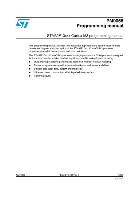
Figure 1.<br />
STM32 Cortex-M3 implementation<br />
STM32 Cortex-M3<br />
processor<br />
NVIC<br />
Processor<br />
core<br />
Embedded<br />
Trace Macrocell<br />
Debug<br />
access<br />
port<br />
Flash<br />
patch<br />
Data<br />
watchpoints<br />
Serial<br />
wire<br />
viewer<br />
Code<br />
interface<br />
Bus matrix<br />
SRAM and<br />
peripheral interface<br />
To facilitate the design of cost-sensitive devices, the Cortex-M3 processor implements<br />
tightly-coupled system components that reduce processor area while significantly improving<br />
interrupt handling and system debug capabilities. The Cortex-M3 processor implements a<br />
version of the Thumb ® instruction set, ensuring high code density and reduced program<br />
memory requirements. The Cortex-M3 instruction set provides the exceptional performance<br />
expected of a modern 32-bit architecture, with the high code density of 8-bit and 16-bit<br />
microcontrollers.<br />
The Cortex-M3 processor closely integrates a configurable nested interrupt controller<br />
(NVIC), to deliver industry-leading interrupt performance. The NVIC includes a nonmaskable<br />
interrupt (NMI), and provides up to 256 interrupt priority levels. The tight<br />
integration of the processor core and NVIC provides fast execution of interrupt service<br />
routines (ISRs), dramatically reducing the interrupt latency. This is achieved through the<br />
hardware stacking of registers, and the ability to suspend load-multiple and store-multiple<br />
operations. Interrupt handlers do not require any assembler stubs, removing any code<br />
overhead from the ISRs. Tail-chaining optimization also significantly reduces the overhead<br />
when switching from one ISR to another.<br />
To optimize low-power designs, the NVIC integrates with the sleep modes, that include a<br />
deep sleep function that enables the STM32 to enter STOP or STDBY mode.<br />
1.3.1 System level interface<br />
The Cortex-M3 processor provides multiple interfaces using AMBA ® technology to provide<br />
high speed, low latency memory accesses. It supports unaligned data accesses and<br />
implements atomic bit manipulation that enables faster peripheral controls, system spinlocks<br />
and thread-safe Boolean data handling.<br />
1.3.2 Integrated configurable debug<br />
ai15994<br />
The Cortex-M3 processor implements a complete hardware debug solution. This provides<br />
high system visibility of the processor and memory through either a traditional JTAG port or<br />
a 2-pin Serial Wire Debug (SWD) port that is ideal for small package devices.<br />
Doc ID 15491 Rev 1 9/137
About this document<br />
<strong>PM0056</strong><br />
For system trace the processor integrates an Instrumentation Trace Macrocell (ITM)<br />
alongside data watchpoints and a profiling unit. To enable simple and cost-effective profiling<br />
of the system events these generate, a Serial Wire Viewer (SWV) can export a stream of<br />
software-generated messages, data trace, and profiling information through a single pin.<br />
The optional Embedded Trace Macrocell (ETM) delivers unrivalled instruction trace capture<br />
in an area far smaller than traditional trace units, enabling many low cost MCUs to<br />
implement full instruction trace for the first time.<br />
1.3.3 Cortex-M3 processor features and benefits summary<br />
●<br />
●<br />
●<br />
●<br />
●<br />
●<br />
●<br />
●<br />
●<br />
Tight integration of system peripherals reduces area and development costs<br />
Thumb instruction set combines high code density with 32-bit performance<br />
Code-patch ability for ROM system updates<br />
Power control optimization of system components<br />
Integrated sleep modes for low power consumption<br />
Fast code execution permits slower processor clock or increases sleep mode time<br />
Hardware division and fast multiplier<br />
Deterministic, high-performance interrupt handling for time-critical applications<br />
Extensive debug and trace capabilities:<br />
– Serial Wire Debug and Serial Wire Trace reduce the number of pins required for<br />
debugging and tracing.<br />
10/137 Doc ID 15491 Rev 1
<strong>PM0056</strong><br />
About this document<br />
1.3.4 Cortex-M3 core peripherals<br />
These are:<br />
Nested vectored interrupt controller<br />
The nested vectored interrupt controller (NVIC) is an embedded interrupt controller that<br />
supports low latency interrupt processing.<br />
System control block<br />
The system control block (SCB) is the programmers model interface to the processor. It<br />
provides system implementation information and system control, including<br />
configuration, control, and reporting of system exceptions.<br />
System timer<br />
The system timer, SysTick, is a 24-bit count-down timer. Use this as a Real Time<br />
Operating System (RTOS) tick timer or as a simple counter.<br />
Doc ID 15491 Rev 1 11/137
The Cortex-M3 processor<br />
<strong>PM0056</strong><br />
2 The Cortex-M3 processor<br />
2.1 Programmers model<br />
This section describes the Cortex-M3 programmers model. In addition to the individual core<br />
register descriptions, it contains information about the processor modes and privilege levels<br />
for software execution and stacks.<br />
2.1.1 Processor mode and privilege levels for software execution<br />
The processor modes are:<br />
Thread mode<br />
Handler mode<br />
Used to execute application software. The processor enters Thread<br />
mode when it comes out of reset.<br />
Used to handle exceptions. The processor returns to Thread mode<br />
when it has finished exception processing.<br />
The privilege levels for software execution are:<br />
Unprivileged<br />
Privileged<br />
The software:<br />
● Has limited access to the MSR and MRS instructions, and cannot<br />
use the CPS instruction<br />
● Cannot access the system timer, NVIC, or system control block<br />
● Might have restricted access to memory or peripherals.<br />
Unprivileged software executes at the unprivileged level.<br />
The software can use all the instructions and has access to all<br />
resources.<br />
Privileged software executes at the privileged level.<br />
2.1.2 Stacks<br />
In Thread mode, the CONTROL register controls whether software execution is privileged or<br />
unprivileged, see CONTROL register on page 20. In Handler mode, software execution is<br />
always privileged.<br />
Only privileged software can write to the CONTROL register to change the privilege level for<br />
software execution in Thread mode. Unprivileged software can use the SVC instruction to<br />
make a supervisor call to transfer control to privileged software.<br />
The processor uses a full descending stack. This means the stack pointer indicates the last<br />
stacked item on the stack memory. When the processor pushes a new item onto the stack, it<br />
decrements the stack pointer and then writes the item to the new memory location. The<br />
processor implements two stacks, the main stack and the process stack, with independent<br />
copies of the stack pointer, see Stack pointer on page 14.<br />
12/137 Doc ID 15491 Rev 1
<strong>PM0056</strong><br />
The Cortex-M3 processor<br />
In Thread mode, the CONTROL register controls whether the processor uses the main<br />
stack or the process stack, see CONTROL register on page 20. In Handler mode, the<br />
processor always uses the main stack. The options for processor operations are:<br />
Table 1.<br />
Processor<br />
mode<br />
Summary of processor mode, execution privilege level, and stack use<br />
options<br />
Used to<br />
execute<br />
Privilege level for<br />
software execution<br />
Stack used<br />
Thread Applications Privileged or unprivileged (1) Main stack or process stack (1)<br />
Handler Exception handlers Always privileged Main stack<br />
1. See CONTROL register on page 20.<br />
2.1.3 Core registers<br />
Figure 2.<br />
Processor core registers<br />
R0<br />
R1<br />
R2<br />
Low registers<br />
R3<br />
R4<br />
R5<br />
R6<br />
General-purpose registers<br />
R7<br />
R8<br />
R9<br />
High registers<br />
R10<br />
R11<br />
R12<br />
Stack Pointer<br />
SP (R13)<br />
PSP ‡<br />
MSP ‡<br />
‡ Banked version of SP<br />
Link Register<br />
LR (R14)<br />
Program Counter<br />
PC (R15)<br />
PSR<br />
PRIMASK<br />
Program status register<br />
FAULTMASK<br />
Exception mask registers<br />
Special registers<br />
BASEPRI<br />
CONTROL<br />
CONTROL register<br />
ai15996<br />
Table 2.<br />
Core register set summary<br />
Name Type (1) Required<br />
privilege (2)<br />
Reset<br />
value<br />
Description<br />
R0-R12 read-write Either Unknown General-purpose registers on page 14<br />
MSP read-write Privileged See description Stack pointer on page 14<br />
PSP read-write Either Unknown Stack pointer on page 14<br />
Doc ID 15491 Rev 1 13/137
The Cortex-M3 processor<br />
<strong>PM0056</strong><br />
Table 2.<br />
Core register set summary (continued)<br />
Name Type (1) Required<br />
privilege (2)<br />
Reset<br />
value<br />
Description<br />
LR read-write Either 0xFFFFFFFF Link register on page 14<br />
PC read-write Either See description Program counter on page 14<br />
PSR read-write Privileged 0x01000000 Program status register on page 15<br />
ASPR read-write Either 0x00000000<br />
IPSR read-only Privileged 0x00000000<br />
EPSR read-only Privileged 0x01000000<br />
Application program status register on<br />
page 16<br />
Interrupt program status register on<br />
page 17<br />
Execution program status register on<br />
page 18<br />
PRIMASK read-write Privileged 0x00000000 Priority mask register on page 19<br />
FAULTMASK read-write Privileged 0x00000000 Fault mask register on page 19<br />
BASEPRI read-write Privileged 0x00000000 Base priority mask register on page 20<br />
CONTROL read-write Privileged 0x00000000 CONTROL register on page 20<br />
1. Describes access type during program execution in thread mode and Handler mode. Debug access can<br />
differ.<br />
2. An entry of Either means privileged and unprivileged software can access the register.<br />
General-purpose registers<br />
R0-R12 are 32-bit general-purpose registers for data operations.<br />
Stack pointer<br />
The Stack Pointer (SP) is register R13. In Thread mode, bit[1] of the CONTROL register<br />
indicates the stack pointer to use:<br />
● 0 = Main Stack Pointer (MSP). This is the reset value.<br />
● 1 = Process Stack Pointer (PSP).<br />
On reset, the processor loads the MSP with the value from address 0x00000000.<br />
Link register<br />
The Link Register (LR) is register R14. It stores the return information for subroutines,<br />
function calls, and exceptions. On reset, the processor loads the LR value 0xFFFFFFFF.<br />
Program counter<br />
The Program Counter (PC) is register R15. It contains the current program address. Bit[0] is<br />
always 0 because instruction fetches must be halfword aligned. On reset, the processor<br />
loads the PC with the value of the reset vector, which is at address 0x00000004.<br />
14/137 Doc ID 15491 Rev 1
<strong>PM0056</strong><br />
The Cortex-M3 processor<br />
Program status register<br />
The Program Status Register (PSR) combines:<br />
●<br />
●<br />
Application Program Status Register (APSR)<br />
Interrupt Program Status Register (IPSR)<br />
● Execution Program Status Register (EPSR)<br />
These registers are mutually exclusive bitfields in the 32-bit PSR. The bit assignments are<br />
as shown in Figure 3 and Figure 4.<br />
Figure 3.<br />
APSR, IPSR and EPSR bit assignments<br />
31 30 29 28 27 26 25 24 23<br />
16 15 10 9<br />
8<br />
0<br />
APSR<br />
N Z C V<br />
Q<br />
Reserved<br />
IPSR<br />
Reserved<br />
ISR_NUMBER<br />
EPSR Reserved ICI/IT T Reserved<br />
ICI/IT<br />
Reserved<br />
Figure 4.<br />
PSR bit assignments<br />
31 30 29 28 27 26 25 24 23 16 15 10 9 8 0<br />
N<br />
Z C V Q ICI/IT T Reserved ICI/IT ISR_NUMBER<br />
Reserved<br />
Access these registers individually or as a combination of any two or all three registers,<br />
using the register name as an argument to the MSR or MRS instructions. For example:<br />
● Read all of the registers using PSR with the MRS instruction<br />
● Write to the APSR using APSR with the MSR instruction.<br />
The PSR combinations and attributes are:<br />
Table 3.<br />
PSR register combinations<br />
Register Type Combination<br />
(1), (2)<br />
PSR read-write<br />
APSR, EPSR, and IPSR<br />
IEPSR read-only EPSR and IPSR<br />
IAPSR read-write (1) APSR and IPSR<br />
EAPSR read-write (2) APSR and EPSR<br />
1. The processor ignores writes to the IPSR bits.<br />
2. Reads of the EPSR bits return zero, and the processor ignores writes to the these bits<br />
See the instruction descriptions MRS on page 99 and MSR on page 100 for more<br />
information about how to access the program status registers.<br />
Doc ID 15491 Rev 1 15/137
The Cortex-M3 processor<br />
<strong>PM0056</strong><br />
Application program status register<br />
The APSR contains the current state of the condition flags from previous instruction<br />
executions. See the register summary in Table 2 on page 13 for its attributes. The bit<br />
assignments are:<br />
Table 4.<br />
Bits<br />
APSR bit definitions<br />
Description<br />
Bit 31<br />
Bit 30<br />
Bit 29<br />
Bit 28<br />
Bit 27<br />
Bits 26:0<br />
N: Negative or less than flag:<br />
0: Operation result was positive, zero, greater than, or equal<br />
1: Operation result was negative or less than.<br />
Z: Zero flag:<br />
0: Operation result was not zero<br />
1: Operation result was zero.<br />
C: Carry or borrow flag:<br />
0: Add operation did not result in a carry bit or subtract operation resulted in a<br />
borrow bit<br />
1: Add operation resulted in a carry bit or subtract operation did not result in a<br />
borrow bit.<br />
V: Overflow flag:<br />
0: Operation did not result in an overflow<br />
1: Operation resulted in an overflow.<br />
Q: Sticky saturation flag:<br />
0: Indicates that saturation has not occurred since reset or since the bit was last<br />
cleared to zero<br />
1: Indicates when an SSAT or USAT instruction results in saturation.<br />
This bit is cleared to zero by software using an MRS instruction.<br />
Reserved.<br />
16/137 Doc ID 15491 Rev 1
<strong>PM0056</strong><br />
The Cortex-M3 processor<br />
Interrupt program status register<br />
The IPSR contains the exception type number of the current Interrupt Service Routine<br />
(ISR). See the register summary in Table 2 on page 13 for its attributes. The bit assignments<br />
are:<br />
Table 5.<br />
Bits<br />
IPSR bit definitions<br />
Description<br />
Bits 31:9<br />
Bits 8:0<br />
Reserved<br />
ISR_NUMBER:<br />
This is the number of the current exception:<br />
0: Thread mode<br />
1: Reserved<br />
2: NMI<br />
3: Hard fault<br />
4: Memory management fault<br />
5: Bus fault<br />
6: Usage fault<br />
7: Reserved<br />
....<br />
10: Reserved<br />
11: SVCall<br />
12: Reserved for Debug<br />
13: Reserved<br />
14: PendSV<br />
15: SysTick<br />
16: IRQ0 (1)<br />
....<br />
....<br />
83: IRQ67 (1)<br />
see Exception types on page 32 for more information.<br />
1. See STM32 product reference <strong>manual</strong>/datasheet for more information on interrupt mapping<br />
Doc ID 15491 Rev 1 17/137
The Cortex-M3 processor<br />
<strong>PM0056</strong><br />
Execution program status register<br />
The EPSR contains the Thumb state bit, and the execution state bits for either the:<br />
●<br />
If-Then (IT) instruction<br />
● Interruptible-Continuable Instruction (ICI) field for an interrupted load multiple or store<br />
multiple instruction.<br />
See the register summary in Table 2 on page 13 for the EPSR attributes. The bit<br />
assignments are:<br />
Table 6.<br />
EPSR bit definitions<br />
Bits<br />
Description<br />
Bits 31:27<br />
Bits 26:25, 15:10<br />
Reserved.<br />
ICI: Interruptible-continuable instruction bits<br />
See Interruptible-continuable instructions on page 18.<br />
Bits 26:25, 15:10 IT: Indicates the execution state bits of the IT instruction, see IT on page 93.<br />
Bit 24 Always set to 1.<br />
Bits 23:16<br />
Bits 9:0]<br />
Reserved.<br />
Reserved.<br />
Attempts to read the EPSR directly through application software using the MSR instruction<br />
always return zero. Attempts to write the EPSR using the MSR instruction in application<br />
software are ignored. Fault handlers can examine EPSR value in the stacked PSR to<br />
indicate the operation that is at fault. See Section 2.3.7: Exception entry and return on<br />
page 36<br />
Interruptible-continuable instructions<br />
When an interrupt occurs during the execution of an LDM or STM instruction, the processor:<br />
● Stops the load multiple or store multiple instruction operation temporarily<br />
● Stores the next register operand in the multiple operation to EPSR bits[15:12].<br />
After servicing the interrupt, the processor:<br />
● Returns to the register pointed to by bits[15:12]<br />
● Resumes execution of the multiple load or store instruction.<br />
When the EPSR holds ICI execution state, bits[26:25,11:10] are zero.<br />
If-Then block<br />
The If-Then block contains up to four instructions following a 16-bit IT instruction. Each<br />
instruction in the block is conditional. The conditions for the instructions are either all the<br />
same, or some can be the inverse of others. See IT on page 93 for more information.<br />
Exception mask registers<br />
The exception mask registers disable the handling of exceptions by the processor. Disable<br />
exceptions where they might impact on timing critical tasks.<br />
18/137 Doc ID 15491 Rev 1
<strong>PM0056</strong><br />
The Cortex-M3 processor<br />
To access the exception mask registers use the MSR and MRS instructions, or the CPS<br />
instruction to change the value of PRIMASK or FAULTMASK. See MRS on page 99, MSR<br />
on page 100, and CPS on page 97 for more information.<br />
Priority mask register<br />
The PRIMASK register prevents activation of all exceptions with configurable priority. See<br />
the register summary in Table 2 on page 13 for its attributes. Figure 5 shows the bit<br />
assignments.<br />
Figure 5.<br />
PRIMASK bit assignments<br />
31<br />
1 0<br />
Reserved<br />
PRIMASK<br />
Table 7.<br />
Bits<br />
Bits 31:1<br />
Bit 0<br />
PRIMASK register bit definitions<br />
Reserved<br />
Description<br />
PRIMASK:<br />
0: No effect<br />
1: Prevents the activation of all exceptions with configurable priority.<br />
Fault mask register<br />
The FAULTMASK register prevents activation of all exceptions except for Non-Maskable<br />
Interrupt (NMI). See the register summary in Table 2 on page 13 for its attributes. Figure 6<br />
shows the bit assignments.<br />
Figure 6.<br />
31<br />
FAULTMASK bit assignments<br />
Reserved<br />
1<br />
0<br />
FAULTMASK<br />
Table 8.<br />
Bits<br />
Bits 31:1<br />
Bit 0<br />
FAULTMASK register bit definitions<br />
Reserved<br />
Function<br />
FAULTMASK:<br />
0: No effect<br />
1: Prevents the activation of all exceptions except for NMI.<br />
The processor clears the FAULTMASK bit to 0 on exit from any exception handler except the<br />
NMI handler.<br />
Doc ID 15491 Rev 1 19/137
The Cortex-M3 processor<br />
<strong>PM0056</strong><br />
Base priority mask register<br />
The BASEPRI register defines the minimum priority for exception processing. When<br />
BASEPRI is set to a nonzero value, it prevents the activation of all exceptions with same or<br />
lower priority level as the BASEPRI value. See the register summary in Table 2 on page 13<br />
for its attributes. Figure 7 shows the bit assignments.<br />
Figure 7.<br />
BASEPRI bit assignments<br />
31 8 7<br />
0<br />
Reserved<br />
BASEPRI<br />
Table 9.<br />
Bits<br />
Bits 31:8<br />
BASEPRI register bit assignments<br />
Function<br />
Reserved<br />
Bits 7:4 BASEPRI[7:4] Priority mask bits (1)<br />
0x00: no effect<br />
Nonzero: defines the base priority for exception processing.<br />
The processor does not process any exception with a priority value greater than or<br />
equal to BASEPRI.<br />
Bits 3:0<br />
Reserved<br />
1. This field is similar to the priority fields in the interrupt priority registers. See Interrupt priority registers<br />
(NVIC_IPRx) on page 111 for more information. Remember that higher priority field values correspond to<br />
lower exception priorities.<br />
CONTROL register<br />
The CONTROL register controls the stack used and the privilege level for software<br />
execution when the processor is in Thread mode. See the register summary in Table 2 on<br />
page 13 for its attributes. Figure 8 shows the bit assignments.<br />
Figure 8.<br />
CONTROL bit assignments<br />
31 2 1 0<br />
Reserved<br />
Active stack pointer<br />
Thread mode privilege level<br />
Table 10.<br />
Bits<br />
Bits 31:2<br />
Bit 1<br />
CONTROL register bit definitions<br />
Function<br />
Reserved<br />
ASPSEL: Active stack pointer selection<br />
Selects the current stack:<br />
0: MSP is the current stack pointer<br />
1: PSP is the current stack pointer.<br />
In Handler mode this bit reads as zero and ignores writes.<br />
20/137 Doc ID 15491 Rev 1
<strong>PM0056</strong><br />
The Cortex-M3 processor<br />
Table 10.<br />
Bits<br />
Bit 0<br />
CONTROL register bit definitions (continued)<br />
Function<br />
TPL: Thread mode privilege level<br />
Defines the Thread mode privilege level.<br />
0: Privileged<br />
1: Unprivileged.<br />
Handler mode always uses the MSP, so the processor ignores explicit writes to the active<br />
stack pointer bit of the CONTROL register when in Handler mode. The exception entry and<br />
return mechanisms update the CONTROL register.<br />
In an OS environment, it is recommended that threads running in Thread mode use the<br />
process stack and the kernel and exception handlers use the main stack.<br />
By default, Thread mode uses the MSP. To switch the stack pointer used in Thread mode to<br />
the PSP, use the MSR instruction to set the Active stack pointer bit to 1, see MSR on<br />
page 100.<br />
When changing the stack pointer, software must use an ISB instruction immediately after<br />
the MSR instruction. This ensures that instructions after the ISB execute using the new<br />
stack pointer. See ISB on page 99<br />
2.1.4 Exceptions and interrupts<br />
The Cortex-M3 processor supports interrupts and system exceptions. The processor and<br />
the Nested Vectored Interrupt Controller (NVIC) prioritize and handle all exceptions. An<br />
exception changes the normal flow of software control. The processor uses handler mode to<br />
handle all exceptions except for reset. See Exception entry on page 37 and Exception return<br />
on page 38 for more information.<br />
The NVIC registers control interrupt handling. See Nested vectored interrupt controller<br />
(NVIC) on page 104 for more information.<br />
2.1.5 Data types<br />
The processor:<br />
●<br />
●<br />
●<br />
Supports the following data types:<br />
– 32-bit words<br />
– 16-bit halfwords<br />
– 8-bit bytes<br />
supports 64-bit data transfer instructions.<br />
manages all memory accesses (data memory, instruction memory and Private<br />
Peripheral Bus (PPB)) as little-endian. See Memory regions, types and attributes on<br />
page 24 for more information.<br />
Doc ID 15491 Rev 1 21/137
The Cortex-M3 processor<br />
<strong>PM0056</strong><br />
2.1.6 The Cortex microcontroller software interface standard (CMSIS)<br />
For a Cortex-M3 microcontroller system, the Cortex Microcontroller Software Interface<br />
Standard (CMSIS) defines:<br />
● A common way to:<br />
– Access peripheral registers<br />
– Define exception vectors<br />
● The names of:<br />
– The registers of the core peripherals<br />
– The core exception vectors<br />
● A device-independent interface for RTOS kernels, including a debug channel<br />
The CMSIS includes address definitions and data structures for the core peripherals in the<br />
Cortex-M3 processor. It also includes optional interfaces for middleware components<br />
comprising a TCP/IP stack and a Flash file system.<br />
CMSIS simplifies software development by enabling the reuse of template code and the<br />
combination of CMSIS-compliant software components from various middleware vendors.<br />
Software vendors can expand the CMSIS to include their peripheral definitions and access<br />
functions for those peripherals.<br />
This document includes the register names defined by the CMSIS, and gives short<br />
descriptions of the CMSIS functions that address the processor core and the core<br />
peripherals.<br />
This document uses the register short names defined by the CMSIS. In a few cases these<br />
differ from the architectural short names that might be used in other documents.<br />
The following sections give more information about the CMSIS:<br />
● Section 2.5.4: Power management programming hints on page 43<br />
● Intrinsic functions on page 49<br />
● The CMSIS mapping of the Cortex-M3 NVIC registers on page 105<br />
● NVIC programming hints on page 113<br />
22/137 Doc ID 15491 Rev 1
<strong>PM0056</strong><br />
The Cortex-M3 processor<br />
2.2 Memory model<br />
This section describes the processor memory map, the behavior of memory accesses, and<br />
the bit-banding features. The processor has a fixed memory map that provides up to 4 GB of<br />
addressable memory.<br />
Figure 9.<br />
Memory map<br />
0xFFFFFFFF<br />
Vendor-specific<br />
memory<br />
Private peripheral<br />
bus<br />
511MB<br />
1.0MB<br />
0xE0100000<br />
0xE00FFFFF<br />
0xE0000000<br />
0xDFFFFFFF<br />
External device<br />
1.0GB<br />
0xA0000000<br />
0x9FFFFFFF<br />
0x43FFFFFF<br />
External RAM<br />
1.0GB<br />
32MB Bit band alias<br />
0x42000000<br />
0x60000000<br />
0x5FFFFFFF<br />
0x400FFFFF<br />
1MB<br />
0x40000000<br />
0x23FFFFFF<br />
Bit band region<br />
Peripheral<br />
0.5GB<br />
0x40000000<br />
0x3FFFFFFF<br />
32MB Bit band alias<br />
SRAM<br />
0.5GB<br />
0x22000000<br />
0x20000000<br />
0x1FFFFFFF<br />
0x200FFFFF<br />
0x20000000<br />
1MB<br />
Bit band region<br />
Code<br />
0.5GB<br />
0x00000000<br />
The regions for SRAM and peripherals include bit-band regions. Bit-banding provides<br />
atomic operations to bit data, see Section 2.2.5: Bit-banding on page 27.<br />
The processor reserves regions of the Private peripheral bus (PPB) address range for core<br />
peripheral registers, see Section 4.1: About the STM32 core peripherals on page 104.<br />
Doc ID 15491 Rev 1 23/137
The Cortex-M3 processor<br />
<strong>PM0056</strong><br />
2.2.1 Memory regions, types and attributes<br />
The memory map splits the memory map into regions. Each region has a defined memory<br />
type, and some regions have additional memory attributes. The memory type and attributes<br />
determine the behavior of accesses to the region.<br />
The memory types are:<br />
Normal<br />
Device<br />
Strongly-ordered<br />
The processor can re-order transactions for efficiency, or<br />
perform speculative reads.<br />
The processor preserves transaction order relative to other<br />
transactions to Device or Strongly-ordered memory.<br />
The processor preserves transaction order relative to all other<br />
transactions.<br />
The different ordering requirements for Device and Strongly-ordered memory mean that the<br />
memory system can buffer a write to Device memory, but must not buffer a write to Stronglyordered<br />
memory.<br />
The additional memory attributes include:<br />
Execute Never (XN) Means the processor prevents instruction accesses. Any<br />
attempt to fetch an instruction from an XN region causes a<br />
memory management fault exception.<br />
24/137 Doc ID 15491 Rev 1
<strong>PM0056</strong><br />
The Cortex-M3 processor<br />
2.2.2 Memory system ordering of memory accesses<br />
For most memory accesses caused by explicit memory access instructions, the memory<br />
system does not guarantee that the order in which the accesses complete matches the<br />
program order of the instructions, providing this does not affect the behavior of the<br />
instruction sequence. Normally, if correct program execution depends on two memory<br />
accesses completing in program order, software must insert a memory barrier instruction<br />
between the memory access instructions, see Section 2.2.4: Software ordering of memory<br />
accesses on page 26.<br />
However, the memory system does guarantee some ordering of accesses to Device and<br />
Strongly-ordered memory. For two memory access instructions A1 and A2, if A1 occurs<br />
before A2 in program order, the ordering of the memory accesses caused by two<br />
instructions is:<br />
Table 11. Ordering of memory accesses (1)<br />
A2<br />
A1<br />
Normal access<br />
Non-shareable<br />
Device access<br />
Shareable<br />
Strongly ordered<br />
access<br />
Normal access - - - -<br />
Device access, nonshareable<br />
- < - <<br />
Device access, shareable - - < <<br />
Strongly ordered access - < < <<br />
1. - means that the memory system does not guarantee the ordering of the accesses.<br />
< means that accesses are observed in program order, that is, A1 is always observed before A2.<br />
2.2.3 Behavior of memory accesses<br />
The behavior of accesses to each region in the memory map is:<br />
Table 12.<br />
Memory access behavior<br />
Address<br />
range<br />
Memory<br />
region<br />
Memory<br />
type<br />
XN<br />
Description<br />
0x00000000- 0x1FFFFFFF Code Normal (1) -<br />
0x20000000- 0x3FFFFFFF SRAM Normal (1) -<br />
Executable region for program code.<br />
You can also put data here.<br />
Executable region for data. You can<br />
also put code here.<br />
This region includes bit band and bit<br />
band alias areas, see Table 13 on<br />
page 27.<br />
0x40000000- 0x5FFFFFFF Peripheral Device (1) XN (1) This region includes bit band and bit<br />
band alias areas, see Table 14 on<br />
page 27.<br />
0x60000000- 0x9FFFFFFF External<br />
RAM<br />
Normal (1) - Executable region for data.<br />
Doc ID 15491 Rev 1 25/137
The Cortex-M3 processor<br />
<strong>PM0056</strong><br />
Table 12.<br />
Memory access behavior (continued)<br />
Address<br />
range<br />
Memory<br />
region<br />
Memory<br />
type<br />
XN<br />
Description<br />
0xA0000000- 0xDFFFFFFF External<br />
device<br />
Device (1) XN (1) External Device memory<br />
0xE0000000- 0xE00FFFFF<br />
0xE0100000- 0xFFFFFFFF<br />
Private<br />
Peripheral<br />
Bus<br />
Memory<br />
mapped<br />
peripherals<br />
This region includes the NVIC,<br />
Stronglyordered<br />
(1) XN (1) System timer, and system control<br />
block.<br />
Device (1) XN (1) This region includes all the STM32<br />
standard peripherals.<br />
1. See Memory regions, types and attributes on page 24 for more information.<br />
The Code, SRAM, and external RAM regions can hold programs. However, it is<br />
recommended that programs always use the Code region. This is because the processor<br />
has separate buses that enable instruction fetches and data accesses to occur<br />
simultaneously.<br />
2.2.4 Software ordering of memory accesses<br />
The order of instructions in the program flow does not always guarantee the order of the<br />
corresponding memory transactions. This is because:<br />
● The processor can reorder some memory accesses to improve efficiency, providing this<br />
does not affect the behavior of the instruction sequence.<br />
● The processor has multiple bus interfaces<br />
● Memory or devices in the memory map have different wait states<br />
● Some memory accesses are buffered or speculative.<br />
Section 2.2.2: Memory system ordering of memory accesses on page 25 describes the<br />
cases where the memory system guarantees the order of memory accesses. Otherwise, if<br />
the order of memory accesses is critical, software must include memory barrier instructions<br />
to force that ordering. The processor provides the following memory barrier instructions:<br />
DMB<br />
DSB<br />
The Data Memory Barrier (DMB) instruction ensures that outstanding<br />
memory transactions complete before subsequent memory transactions.<br />
See DMB on page 98.<br />
The Data Synchronization Barrier (DSB) instruction ensures that<br />
outstanding memory transactions complete before subsequent<br />
instructions execute. See DSB on page 98.<br />
ISB<br />
The Instruction Synchronization Barrier (ISB) ensures that the effect of all<br />
completed memory transactions is recognizable by subsequent<br />
instructions. See ISB on page 99.<br />
Use memory barrier instructions in, for example:<br />
● Vector table. If the program changes an entry in the vector table, and then enables the<br />
corresponding exception, use a DMB instruction between the operations. This ensures<br />
that if the exception is taken immediately after being enabled the processor uses the<br />
new exception vector.<br />
26/137 Doc ID 15491 Rev 1
<strong>PM0056</strong><br />
The Cortex-M3 processor<br />
● Self-modifying code. If a program contains self-modifying code, use an ISB<br />
instruction immediately after the code modification in the program. This ensures<br />
subsequent instruction execution uses the updated program.<br />
● Memory map switching. If the system contains a memory map switching mechanism,<br />
use a DSB instruction after switching the memory map in the program. This ensures<br />
subsequent instruction execution uses the updated memory map.<br />
● Dynamic exception priority change. When an exception priority has to change when<br />
the exception is pending or active, use DSB instructions after the change. This ensures<br />
the change takes effect on completion of the DSB instruction.<br />
● Using a semaphore in multi-master system. If the system contains more than one<br />
bus master, for example, if another processor is present in the system, each processor<br />
must use a DMB instruction after any semaphore instructions, to ensure other bus<br />
masters see the memory transactions in the order in which they were executed.<br />
Memory accesses to Strongly-ordered memory, such as the system control block, do not<br />
require the use of DMB instructions.<br />
2.2.5 Bit-banding<br />
A bit-band region maps each word in a bit-band alias region to a single bit in the bit-band<br />
region. The bit-band regions occupy the lowest 1 MB of the SRAM and peripheral memory<br />
regions.<br />
The memory map has two 32 MB alias regions that map to two 1 MB bit-band regions:<br />
● Accesses to the 32 MB SRAM alias region map to the 1 MB SRAM bit-band region, as<br />
shown in Table 13<br />
●<br />
Accesses to the 32 MB peripheral alias region map to the 1 MB peripheral bit-band<br />
region, as shown in Table 14.<br />
Table 13.<br />
Address<br />
range<br />
SRAM memory bit-banding regions<br />
Memory<br />
region<br />
Instruction and data accesses<br />
0x20000000-<br />
0x200FFFFF<br />
0x22000000-<br />
0x23FFFFFF<br />
SRAM bit-band region<br />
SRAM bit-band alias<br />
Direct accesses to this memory range behave as SRAM memory<br />
accesses, but this region is also bit addressable through bit-band alias.<br />
Data accesses to this region are remapped to bit band region. A write<br />
operation is performed as read-modify-write. Instruction accesses are not<br />
remapped.<br />
Table 14.<br />
Address<br />
range<br />
Peripheral memory bit-banding regions<br />
Memory<br />
region<br />
Instruction and data accesses<br />
0x40000000-<br />
0x400FFFFF<br />
0x42000000-<br />
0x43FFFFFF<br />
Peripheral bit-band alias<br />
Peripheral bit-band<br />
region<br />
Direct accesses to this memory range behave as peripheral memory<br />
accesses, but this region is also bit addressable through bit-band<br />
alias.<br />
Data accesses to this region are remapped to bit band region. A write<br />
operation is performed as read-modify-write. Instruction accesses are<br />
not permitted.<br />
Doc ID 15491 Rev 1 27/137
The Cortex-M3 processor<br />
<strong>PM0056</strong><br />
A word access to the SRAM or peripheral bit-band alias regions map to a single bit in the<br />
SRAM or peripheral bit-band region.<br />
The following formula shows how the alias region maps onto the bit-band region:<br />
bit_word_offset = (byte_offset x 32) + (bit_number x 4)<br />
bit_word_addr = bit_band_base + bit_word_offset<br />
Where:<br />
● Bit_word_offset is the position of the target bit in the bit-band memory region.<br />
● Bit_word_addr is the address of the word in the alias memory region that maps to the<br />
targeted bit.<br />
● Bit_band_base is the starting address of the alias region.<br />
● Byte_offset is the number of the byte in the bit-band region that contains the targeted<br />
bit.<br />
● Bit_number is the bit position, 0-7, of the targeted bit.<br />
Figure 10 on page 28 shows examples of bit-band mapping between the SRAM bit-band<br />
alias region and the SRAM bit-band region:<br />
● The alias word at 0x23FFFFE0 maps to bit[0] of the bit-band byte at<br />
0x200FFFFF: 0x23FFFFE0 = 0x22000000 + (0xFFFFF*32) + (0*4).<br />
● The alias word at 0x23FFFFFC maps to bit[7] of the bit-band byte at<br />
0x200FFFFF: 0x23FFFFFC = 0x22000000 + (0xFFFFF*32) + (7*4).<br />
● The alias word at 0x22000000 maps to bit[0] of the bit-band byte at<br />
0x20000000: 0x22000000 = 0x22000000 + (0*32) + (0 *4).<br />
● The alias word at 0x2200001C maps to bit[7] of the bit-band byte at<br />
0x20000000: 0x2200001C = 0x22000000+ (0*32) + (7*4).<br />
Figure 10.<br />
Bit-band mapping<br />
32MB alias region<br />
0x23FFFFFC<br />
0x23FFFFF8<br />
0x23FFFFF4<br />
0x23FFFFF0<br />
0x23FFFFEC<br />
0x23FFFFE8<br />
0x23FFFFE4<br />
0x23FFFFE0<br />
0x2200001C<br />
0x22000018<br />
0x22000014<br />
0x22000010<br />
0x2200000C<br />
0x22000008<br />
0x22000004<br />
0x22000000<br />
1MB SRAM bit-band region<br />
7 6 5 4 3 2 1 0 7 6 5 4 3 2 1 0<br />
7 6 5 4 3 2 1 0 7 6 5 4 3 2 1 0<br />
0x200FFFFF<br />
0x200FFFFE<br />
0x200FFFFD<br />
0x200FFFFC<br />
7<br />
6 5 4 3 2 1 0 7 6 5 4 3 2 1 0 7 6 5 4 3 2 1 0 7 6 5 4 3 2 1 0<br />
0x20000003<br />
0x20000002<br />
0x20000001<br />
0x20000000<br />
28/137 Doc ID 15491 Rev 1
<strong>PM0056</strong><br />
The Cortex-M3 processor<br />
Directly accessing an alias region<br />
Writing to a word in the alias region updates a single bit in the bit-band region.<br />
Bit[0] of the value written to a word in the alias region determines the value written to the<br />
targeted bit in the bit-band region. Writing a value with bit[0] set to 1 writes a 1 to the bitband<br />
bit, and writing a value with bit[0] set to 0 writes a 0 to the bit-band bit.<br />
Bits[31:1] of the alias word have no effect on the bit-band bit. Writing 0x01 has the same<br />
effect as writing 0xFF. Writing 0x00 has the same effect as writing 0x0E.<br />
Reading a word in the alias region:<br />
●<br />
0x00000000 indicates that the targeted bit in the bit-band region is set to zero<br />
● 0x00000001 indicates that the targeted bit in the bit-band region is set to 1<br />
Directly accessing a bit-band region<br />
Behavior of memory accesses on page 25 describes the behavior of direct byte, halfword, or<br />
word accesses to the bit-band regions.<br />
2.2.6 Memory endianness<br />
The processor views memory as a linear collection of bytes numbered in ascending order<br />
from zero. For example, bytes 0-3 hold the first stored word, and bytes 4-7 hold the second<br />
stored word.<br />
Little-endian format<br />
In little-endian format, the processor stores the least significant byte of a word at the lowestnumbered<br />
byte, and the most significant byte at the highest-numbered byte. See Figure 11<br />
for an example.<br />
Figure 11.<br />
Little-endian example<br />
Memory<br />
Register<br />
7<br />
0<br />
31 24 23 16 15 8 7 0<br />
Address A<br />
B0<br />
lsbyte<br />
B3<br />
B2<br />
B1<br />
B0<br />
A+1<br />
B1<br />
A+2<br />
B2<br />
A+3<br />
B3<br />
msbyte<br />
Doc ID 15491 Rev 1 29/137
The Cortex-M3 processor<br />
<strong>PM0056</strong><br />
2.2.7 Synchronization primitives<br />
The Cortex-M3 instruction set includes pairs of synchronization primitives. These provide a<br />
non-blocking mechanism that a thread or process can use to obtain exclusive access to a<br />
memory location. Software can use them to perform a guaranteed read-modify-write<br />
memory update sequence, or for a semaphore mechanism.<br />
A pair of synchronization primitives comprises:<br />
A Load-Exclusive instruction Used to read the value of a memory location, requesting<br />
exclusive access to that location.<br />
A Store-Exclusive instruction Used to attempt to write to the same memory location,<br />
returning a status bit to a register. If this bit is:<br />
0: it indicates that the thread or process gained<br />
exclusive access to the memory, and the write<br />
succeeds<br />
1: it indicates that the thread or process did not gain<br />
exclusive access to the memory, and no write is<br />
performed<br />
The pairs of Load-Exclusive and Store-Exclusive instructions are:<br />
● The word instructions LDREX and STREX<br />
● The halfword instructions LDREXH and STREXH<br />
● The byte instructions LDREXB and STREXB.<br />
Software must use a Load-Exclusive instruction with the corresponding Store-Exclusive<br />
instruction.<br />
To perform a guaranteed read-modify-write of a memory location, software must:<br />
1. Use a Load-Exclusive instruction to read the value of the location.<br />
2. Update the value, as required.<br />
3. Use a Store-Exclusive instruction to attempt to write the new value back to the memory<br />
location, and tests the returned status bit. If this bit is:<br />
0: The read-modify-write completed successfully,<br />
1: No write was performed. This indicates that the value returned at step 1 might<br />
be out of date. The software must retry the read-modify-write sequence,<br />
30/137 Doc ID 15491 Rev 1
<strong>PM0056</strong><br />
The Cortex-M3 processor<br />
Software can use the synchronization primitives to implement a semaphores as follows:<br />
1. Use a Load-Exclusive instruction to read from the semaphore address to check<br />
whether the semaphore is free.<br />
2. If the semaphore is free, use a Store-Exclusive to write the claim value to the<br />
semaphore address.<br />
3. If the returned status bit from step 2 indicates that the Store-Exclusive succeeded then<br />
the software has claimed the semaphore. However, if the Store-Exclusive failed,<br />
another process might have claimed the semaphore after the software performed step<br />
1.<br />
The Cortex-M3 includes an exclusive access monitor, that tags the fact that the processor<br />
has executed a Load-Exclusive instruction.<br />
The processor removes its exclusive access tag if:<br />
● It executes a CLREX instruction<br />
● It executes a Store-Exclusive instruction, regardless of whether the write succeeds.<br />
● An exception occurs. This means the processor can resolve semaphore conflicts<br />
between different threads.<br />
For more information about the synchronization primitive instructions, see LDREX and<br />
STREX on page 69 and CLREX on page 70.<br />
2.2.8 <strong>Programming</strong> hints for the synchronization primitives<br />
ANSI C cannot directly generate the exclusive access instructions. Some C compilers<br />
provide intrinsic functions for generation of these instructions:<br />
Table 15.<br />
Instruction<br />
C compiler intrinsic functions for exclusive access instructions<br />
Intrinsic function<br />
LDREX, LDREXH, or LDREXB<br />
STREX, STREXH, or STREXB<br />
CLREX<br />
unsigned int __ldrex(volatile void *ptr)<br />
int __strex(unsigned int val, volatile void *ptr)<br />
void __clrex(void)<br />
The actual exclusive access instruction generated depends on the data type of the pointer<br />
passed to the intrinsic function. For example, the following C code generates the require<br />
LDREXB operation:<br />
__ldrex((volatile char *) 0xFF);<br />
Doc ID 15491 Rev 1 31/137
The Cortex-M3 processor<br />
<strong>PM0056</strong><br />
2.3 Exception model<br />
This section describes the exception model.<br />
2.3.1 Exception states<br />
Each exception is in one of the following states:<br />
Inactive<br />
Pending<br />
Active<br />
The exception is not active and not pending.<br />
The exception is waiting to be serviced by the processor. An<br />
interrupt request from a peripheral or from software can change<br />
the state of the corresponding interrupt to pending.<br />
An exception that is being serviced by the processor but has not<br />
completed.<br />
Note: An exception handler can interrupt the execution of another<br />
exception handler. In this case both exceptions are in the active<br />
state.<br />
Active and pending The exception is being serviced by the processor and there is a<br />
pending exception from the same source.<br />
2.3.2 Exception types<br />
The exception types are:<br />
Reset<br />
NMI<br />
Hard fault<br />
Reset is invoked on power up or a warm reset. The exception model<br />
treats reset as a special form of exception. When reset is asserted,<br />
the operation of the processor stops, potentially at any point in an<br />
instruction. When reset is deasserted, execution restarts from the<br />
address provided by the reset entry in the vector table. Execution<br />
restarts as privileged execution in Thread mode.<br />
A NonMaskable Interrupt (NMI) can be signalled by a peripheral or<br />
triggered by software. This is the highest priority exception other<br />
than reset. It is permanently enabled and has a fixed priority of -2.<br />
NMIs cannot be:<br />
● Masked or prevented from activation by any other exception<br />
● Preempted by any exception other than Reset.<br />
A hard fault is an exception that occurs because of an error during<br />
exception processing, or because an exception cannot be managed<br />
by any other exception mechanism. Hard faults have a fixed priority<br />
of -1, meaning they have higher priority than any exception with<br />
configurable priority.<br />
Memory management<br />
fault<br />
A memory management fault is an exception that occurs because of<br />
a memory protection related fault. The fixed memory protection<br />
constraints determines this fault, for both instruction and data<br />
memory transactions. This fault is used to abort instruction accesses<br />
to Execute Never (XN) memory regions.<br />
32/137 Doc ID 15491 Rev 1
<strong>PM0056</strong><br />
The Cortex-M3 processor<br />
Bus fault<br />
Usage fault<br />
SVCall<br />
PendSV<br />
SysTick<br />
Interrupt (IRQ)<br />
A bus fault is an exception that occurs because of a memory related<br />
fault for an instruction or data memory transaction. This might be<br />
from an error detected on a bus in the memory system.<br />
A usage fault is an exception that occurs because of a fault related to<br />
instruction execution. This includes:<br />
● An undefined instruction<br />
● An illegal unaligned access<br />
● Invalid state on instruction execution<br />
● An error on exception return.<br />
The following can cause a usage fault when the core is configured to<br />
report them:<br />
● An unaligned address on word and halfword memory access<br />
● Division by zero<br />
A supervisor call (SVC) is an exception that is triggered by the SVC<br />
instruction. In an OS environment, applications can use SVC<br />
instructions to access OS kernel functions and device drivers.<br />
PendSV is an interrupt-driven request for system-level service. In an<br />
OS environment, use PendSV for context switching when no other<br />
exception is active.<br />
A SysTick exception is an exception the system timer generates<br />
when it reaches zero. Software can also generate a SysTick<br />
exception. In an OS environment, the processor can use this<br />
exception as system tick.<br />
A interrupt, or IRQ, is an exception signalled by a peripheral, or<br />
generated by a software request. All interrupts are asynchronous to<br />
instruction execution. In the system, peripherals use interrupts to<br />
communicate with the processor.<br />
Table 16.<br />
Properties of the different exception types<br />
Exception<br />
number (1)<br />
IRQ<br />
number (1)<br />
Exception<br />
type<br />
Priority<br />
Vector address<br />
or offset (2)<br />
Activation<br />
1 - Reset -3, the highest 0x00000004 Asynchronous<br />
2 -14 NMI -2 0x00000008 Asynchronous<br />
3 -13 Hard fault -1 0x0000000C -<br />
4 -12<br />
Memory<br />
management fault<br />
Configurable (3) 0x00000010 Synchronous<br />
5 -11 Bus fault Configurable (3) 0x00000014<br />
Synchronous when precise,<br />
asynchronous when imprecise<br />
6 -10 Usage fault Configurable (3) 0x00000018 Synchronous<br />
7-10 - - - Reserved -<br />
11 -5 SVCall Configurable (3) 0x0000002C Synchronous<br />
12-13 - - - Reserved -<br />
Doc ID 15491 Rev 1 33/137
The Cortex-M3 processor<br />
<strong>PM0056</strong><br />
Table 16.<br />
Properties of the different exception types (continued)<br />
Exception<br />
number (1)<br />
IRQ<br />
number (1)<br />
Exception<br />
type<br />
Priority<br />
Vector address<br />
or offset (2)<br />
Activation<br />
14 -2 PendSV Configurable (3) 0x00000038 Asynchronous<br />
15 -1 SysTick Configurable (3) 0x0000003C Asynchronous<br />
16-83 0-67 Interrupt (IRQ) Configurable (4) 0x00000040 and<br />
above (5)<br />
Asynchronous<br />
1. To simplify the software layer, the CMSIS only uses IRQ numbers and therefore uses negative values for exceptions other<br />
than interrupts. The IPSR returns the Exception number, see Interrupt program status register on page 17.<br />
2. See Vector table on page 35 for more information.<br />
3. See System handler priority registers (SHPRx) on page 122.<br />
4. See Interrupt priority registers (NVIC_IPRx) on page 111.<br />
5. Increasing in steps of 4.<br />
For an asynchronous exception, other than reset, the processor can execute another<br />
instruction between when the exception is triggered and when the processor enters the<br />
exception handler.<br />
Privileged software can disable the exceptions that Table 16 on page 33 shows as having<br />
configurable priority, see:<br />
● System handler control and state register (SCB_SHCSR) on page 124<br />
● Interrupt clear-enable registers (NVIC_ICERx) on page 107<br />
For more information about hard faults, memory management faults, bus faults, and usage<br />
faults, see Section 2.4: Fault handling on page 39.<br />
2.3.3 Exception handlers<br />
The processor handles exceptions using:<br />
Interrupt Service<br />
Routines (ISRs)<br />
Fault handlers<br />
System handlers<br />
Interrupts IRQ0 to IRQ67 are the exceptions handled by ISRs.<br />
Hard fault, memory management fault, usage fault, bus fault are fault<br />
exceptions handled by the fault handlers.<br />
NMI, PendSV, SVCall SysTick, and the fault exceptions are all<br />
system exceptions that are handled by system handlers.<br />
34/137 Doc ID 15491 Rev 1
<strong>PM0056</strong><br />
The Cortex-M3 processor<br />
2.3.4 Vector table<br />
The vector table contains the reset value of the stack pointer, and the start addresses, also<br />
called exception vectors, for all exception handlers. Figure 12 on page 35 shows the order of<br />
the exception vectors in the vector table. The least-significant bit of each vector must be 1,<br />
indicating that the exception handler is Thumb code.<br />
Figure 12.<br />
Vector table<br />
Exception number<br />
IRQ number<br />
Offset<br />
Vector<br />
83<br />
67<br />
0x014C<br />
IRQ67<br />
.<br />
.<br />
.<br />
.<br />
.<br />
.<br />
.<br />
.<br />
.<br />
18<br />
17<br />
16<br />
15<br />
14<br />
13<br />
2<br />
1<br />
0<br />
-1<br />
-2<br />
0x004C<br />
0x0048<br />
0x0044<br />
0x0040<br />
0x003C<br />
0x0038<br />
IRQ2<br />
IRQ1<br />
IRQ0<br />
Systick<br />
PendSV<br />
Reserved<br />
12<br />
Reserved for Debug<br />
11<br />
10<br />
-5<br />
0x002C<br />
SVCall<br />
9<br />
8<br />
Reserved<br />
7<br />
6<br />
5<br />
4<br />
3<br />
2<br />
1<br />
-10<br />
-11<br />
-12<br />
-13<br />
-14<br />
0x0018<br />
0x0014<br />
0x0010<br />
0x000C<br />
0x0008<br />
0x0004<br />
0x0000<br />
Usage fault<br />
Bus fault<br />
Memory management fault<br />
Hard fault<br />
NMI<br />
Reset<br />
Initial SP value<br />
ai15995<br />
On system reset, the vector table is fixed at address 0x00000000. Privileged software can<br />
write to the VTOR to relocate the vector table start address to a different memory location, in<br />
the range 0x00000080 to 0x3FFFFF80, see Vector table offset register (SCB_VTOR) on<br />
page 118.<br />
2.3.5 Exception priorities<br />
As Table 16 on page 33 shows, all exceptions have an associated priority, with:<br />
● A lower priority value indicating a higher priority<br />
● Configurable priorities for all exceptions except Reset, Hard fault, and NMI.<br />
Doc ID 15491 Rev 1 35/137
The Cortex-M3 processor<br />
<strong>PM0056</strong><br />
If software does not configure any priorities, then all exceptions with a configurable priority<br />
have a priority of 0. For information about configuring exception priorities see<br />
● System handler priority registers (SHPRx) on page 122<br />
● Interrupt priority registers (NVIC_IPRx) on page 111<br />
Configurable priority values are in the range 0-15. This means that the Reset, Hard fault,<br />
and NMI exceptions, with fixed negative priority values, always have higher priority than any<br />
other exception.<br />
For example, assigning a higher priority value to IRQ[0] and a lower priority value to IRQ[1]<br />
means that IRQ[1] has higher priority than IRQ[0]. If both IRQ[1] and IRQ[0] are asserted,<br />
IRQ[1] is processed before IRQ[0].<br />
If multiple pending exceptions have the same priority, the pending exception with the lowest<br />
exception number takes precedence. For example, if both IRQ[0] and IRQ[1] are pending<br />
and have the same priority, then IRQ[0] is processed before IRQ[1].<br />
When the processor is executing an exception handler, the exception handler is preempted<br />
if a higher priority exception occurs. If an exception occurs with the same priority as the<br />
exception being handled, the handler is not preempted, irrespective of the exception<br />
number. However, the status of the new interrupt changes to pending.<br />
2.3.6 Interrupt priority grouping<br />
To increase priority control in systems with interrupts, the NVIC supports priority grouping.<br />
This divides each interrupt priority register entry into two fields:<br />
● An upper field that defines the group priority<br />
● A lower field that defines a subpriority within the group.<br />
Only the group priority determines preemption of interrupt exceptions. When the processor<br />
is executing an interrupt exception handler, another interrupt with the same group priority as<br />
the interrupt being handled does not preempt the handler,<br />
If multiple pending interrupts have the same group priority, the subpriority field determines<br />
the order in which they are processed. If multiple pending interrupts have the same group<br />
priority and subpriority, the interrupt with the lowest IRQ number is processed first.<br />
For information about splitting the interrupt priority fields into group priority and subpriority,<br />
see Application interrupt and reset control register (SCB_AIRCR) on page 119.<br />
2.3.7 Exception entry and return<br />
Descriptions of exception handling use the following terms:<br />
Preemption<br />
When the processor is executing an exception handler, an exception<br />
can preempt the exception handler if its priority is higher than the<br />
priority of the exception being handled. See Section 2.3.6: Interrupt<br />
priority grouping for more information about preemption by an<br />
interrupt.<br />
When one exception preempts another, the exceptions are called<br />
nested exceptions. See Exception entry on page 37 more<br />
information.<br />
36/137 Doc ID 15491 Rev 1
<strong>PM0056</strong><br />
The Cortex-M3 processor<br />
Return<br />
Tail-chaining<br />
Late-arriving<br />
This occurs when the exception handler is completed, and:<br />
● There is no pending exception with sufficient priority to be<br />
serviced<br />
● The completed exception handler was not handling a latearriving<br />
exception.<br />
The processor pops the stack and restores the processor state to the<br />
state it had before the interrupt occurred. See Exception return on<br />
page 38 for more information.<br />
This mechanism speeds up exception servicing. On completion of an<br />
exception handler, if there is a pending exception that meets the<br />
requirements for exception entry, the stack pop is skipped and<br />
control transfers to the new exception handler.<br />
This mechanism speeds up preemption. If a higher priority exception<br />
occurs during state saving for a previous exception, the processor<br />
switches to handle the higher priority exception and initiates the<br />
vector fetch for that exception. State saving is not affected by late<br />
arrival because the state saved is the same for both exceptions.<br />
Therefore the state saving continues uninterrupted. The processor<br />
can accept a late arriving exception until the first instruction of the<br />
exception handler of the original exception enters the execute stage<br />
of the processor. On return from the exception handler of the latearriving<br />
exception, the normal tail-chaining rules apply.<br />
Exception entry<br />
Exception entry occurs when there is a pending exception with sufficient priority and either:<br />
●<br />
The processor is in Thread mode<br />
● The new exception is of higher priority than the exception being handled, in which case<br />
the new exception preempts the original exception.<br />
When one exception preempts another, the exceptions are nested.<br />
Sufficient priority means the exception has more priority than any limits set by the mask<br />
registers, see Exception mask registers on page 18. An exception with less priority than this<br />
is pending but is not handled by the processor.<br />
When the processor takes an exception, unless the exception is a tail-chained or a latearriving<br />
exception, the processor pushes information onto the current stack. This operation<br />
is referred as stacking and the structure of eight data words is referred as stack frame. The<br />
stack frame contains the following information:<br />
● R0-R3, R12<br />
● Return address<br />
● PSR<br />
● LR.<br />
Immediately after stacking, the stack pointer indicates the lowest address in the stack frame.<br />
Unless stack alignment is disabled, the stack frame is aligned to a double-word address. If<br />
the STKALIGN bit of the Configuration Control Register (CCR) is set to 1, stack align<br />
adjustment is performed during stacking.<br />
Doc ID 15491 Rev 1 37/137
The Cortex-M3 processor<br />
<strong>PM0056</strong><br />
The stack frame includes the return address. This is the address of the next instruction in<br />
the interrupted program. This value is restored to the PC at exception return so that the<br />
interrupted program resumes.<br />
In parallel to the stacking operation, the processor performs a vector fetch that reads the<br />
exception handler start address from the vector table. When stacking is complete, the<br />
processor starts executing the exception handler. At the same time, the processor writes an<br />
EXC_RETURN value to the LR. This indicates which stack pointer corresponds to the stack<br />
frame and what operation mode the was processor was in before the entry occurred.<br />
If no higher priority exception occurs during exception entry, the processor starts executing<br />
the exception handler and automatically changes the status of the corresponding pending<br />
interrupt to active.<br />
If another higher priority exception occurs during exception entry, the processor starts<br />
executing the exception handler for this exception and does not change the pending status<br />
of the earlier exception. This is the late arrival case.<br />
Exception return<br />
Exception return occurs when the processor is in Handler mode and executes one of the<br />
following instructions to load the EXC_RETURN value into the PC:<br />
●<br />
●<br />
A POP instruction that includes the PC<br />
A BX instruction with any register.<br />
● An LDR or LDM instruction with the PC as the destination<br />
EXC_RETURN is the value loaded into the LR on exception entry. The exception<br />
mechanism relies on this value to detect when the processor has completed an exception<br />
handler. The lowest four bits of this value provide information on the return stack and<br />
processor mode. Table 17 shows the EXC_RETURN[3:0] values with a description of the<br />
exception return behavior.<br />
The processor sets EXC_RETURN bits[31:4] to 0xFFFFFFF. When this value is loaded into<br />
the PC it indicates to the processor that the exception is complete, and the processor<br />
initiates the exception return sequence.<br />
Table 17.<br />
Exception return behavior<br />
EXC_RETURN[3:0]<br />
Description<br />
0bxxx0<br />
0b0001<br />
0b0011<br />
0b01x1<br />
0b1001<br />
Reserved.<br />
Return to Handler mode.<br />
Exception return gets state from MSP.<br />
Execution uses MSP after return.<br />
Reserved.<br />
Reserved.<br />
Return to Thread mode.<br />
Exception return gets state from MSP.<br />
Execution uses MSP after return.<br />
38/137 Doc ID 15491 Rev 1
<strong>PM0056</strong><br />
The Cortex-M3 processor<br />
Table 17.<br />
Exception return behavior (continued)<br />
EXC_RETURN[3:0]<br />
Description<br />
0b1101<br />
0b1x11<br />
Return to Thread mode.<br />
Exception return gets state from PSP.<br />
Execution uses PSP after return.<br />
Reserved.<br />
2.4 Fault handling<br />
Faults are a subset of the exceptions, see Exception model on page 32. The following<br />
generate a fault:<br />
● A bus error on:<br />
– An instruction fetch or vector table load<br />
– A data access<br />
● An internally-detected error such as an undefined instruction or an attempt to change<br />
state with a BX instruction<br />
● Attempting to execute an instruction from a memory region marked as Non-Executable<br />
(XN).<br />
2.4.1 Fault types<br />
Table 18 shows the types of fault, the handler used for the fault, the corresponding fault<br />
status register, and the register bit that indicates that the fault has occurred. See<br />
Configurable fault status register (SCB_CFSR) on page 126 for more information about the<br />
fault status registers.<br />
Table 18.<br />
Faults<br />
Fault Handler Bit name Fault status register<br />
Bus error on a vector read<br />
Fault escalated to a hard fault<br />
Hard fault<br />
VECTTBL<br />
FORCED<br />
Hard fault status register<br />
(SCB_HFSR) on page 129<br />
Bus error:<br />
During exception stacking<br />
- -<br />
STKERR<br />
During exception unstacking<br />
During instruction prefetch<br />
Precise data bus error<br />
Bus fault<br />
UNSTKERR<br />
IBUSERR<br />
PRECISERR<br />
Configurable fault status<br />
register (SCB_CFSR) on<br />
page 126<br />
Imprecise data bus error<br />
IMPRECISERR<br />
Doc ID 15491 Rev 1 39/137
The Cortex-M3 processor<br />
<strong>PM0056</strong><br />
Table 18.<br />
Faults (continued)<br />
Fault Handler Bit name Fault status register<br />
Attempt to access a coprocessor<br />
NOCP<br />
Undefined instruction<br />
UNDEFINSTR<br />
Attempt to enter an invalid instruction<br />
set state (1)<br />
Invalid EXC_RETURN value<br />
Usage fault<br />
INVSTATE<br />
INVPC<br />
Configurable fault status<br />
register (SCB_CFSR) on<br />
page 126<br />
Illegal unaligned load or store<br />
UNALIGNED<br />
Divide By 0<br />
DIVBYZERO<br />
1. Attempting to use an instruction set other than the Thumb instruction set.<br />
2.4.2 Fault escalation and hard faults<br />
All faults exceptions except for hard fault have configurable exception priority, see System<br />
handler priority registers (SHPRx) on page 122. Software can disable execution of the<br />
handlers for these faults, see System handler control and state register (SCB_SHCSR) on<br />
page 124.<br />
Usually, the exception priority, together with the values of the exception mask registers,<br />
determines whether the processor enters the fault handler, and whether a fault handler can<br />
preempt another fault handler. as described in Section 2.3: Exception model on page 32.<br />
In some situations, a fault with configurable priority is treated as a hard fault. This is called<br />
priority escalation, and the fault is described as escalated to hard fault. Escalation to hard<br />
fault occurs when:<br />
● A fault handler causes the same kind of fault as the one it is servicing. This escalation<br />
to hard fault occurs because a fault handler cannot preempt itself because it must have<br />
the same priority as the current priority level.<br />
● A fault handler causes a fault with the same or lower priority as the fault it is servicing.<br />
This is because the handler for the new fault cannot preempt the currently executing<br />
fault handler.<br />
● An exception handler causes a fault for which the priority is the same as or lower than<br />
the currently executing exception.<br />
● A fault occurs and the handler for that fault is not enabled.<br />
If a bus fault occurs during a stack push when entering a bus fault handler, the bus fault<br />
does not escalate to a hard fault. This means that if a corrupted stack causes a fault, the<br />
fault handler executes even though the stack push for the handler failed. The fault handler<br />
operates but the stack contents are corrupted.<br />
Only Reset and NMI can preempt the fixed priority hard fault. A hard fault can preempt any<br />
exception other than Reset, NMI, or another hard fault.<br />
40/137 Doc ID 15491 Rev 1
<strong>PM0056</strong><br />
The Cortex-M3 processor<br />
2.4.3 Fault status registers and fault address registers<br />
The fault status registers indicate the cause of a fault. For bus faults and memory<br />
management faults, the fault address register indicates the address accessed by the<br />
operation that caused the fault, as shown in Table 19.<br />
Table 19.<br />
Fault status and fault address registers<br />
Handler<br />
Status register<br />
name<br />
Address register<br />
name<br />
Register description<br />
Hard fault HFSR -<br />
Hard fault status register (SCB_HFSR) on<br />
page 129<br />
Memory<br />
management fault<br />
MMFSR<br />
MMFAR<br />
Configurable fault status register (SCB_CFSR)<br />
on page 126<br />
Memory management fault address register<br />
(SCB_MMFAR) on page 130<br />
Bus fault BFSR BFAR<br />
Usage fault UFSR -<br />
Configurable fault status register (SCB_CFSR)<br />
on page 126<br />
Bus fault address register (SCB_BFAR) on<br />
page 130<br />
Configurable fault status register (SCB_CFSR)<br />
on page 126<br />
2.4.4 Lockup<br />
The processor enters a lockup state if a hard fault occurs when executing the NMI or hard<br />
fault handlers. When the processor is in lockup state it does not execute any instructions.<br />
The processor remains in lockup state until either:<br />
● It is reset<br />
● An NMI occurs<br />
If lockup state occurs from the NMI handler a subsequent NMI does not cause the processor<br />
to leave lockup state.<br />
2.5 Power management<br />
The STM32 and Cortex-M3 processor sleep modes reduce power consumption:<br />
● Sleep mode stops the processor clock. All other system and peripheral clocks may still<br />
be running.<br />
● Deep sleep mode stops most of the STM32 system and peripheral clocks. At product<br />
level, this corresponds to either the Stop or the Standby mode. For more details, please<br />
refer to the “Power modes” Section in the STM32 reference <strong>manual</strong>.<br />
The SLEEPDEEP bit of the SCR selects which sleep mode is used, see System control<br />
register (SCB_SCR) on page 120. For more information about the behavior of the sleep<br />
modes see the STM32 product reference <strong>manual</strong>.<br />
This section describes the mechanisms for entering sleep mode, and the conditions for<br />
waking up from sleep mode.<br />
Doc ID 15491 Rev 1 41/137
The Cortex-M3 processor<br />
<strong>PM0056</strong><br />
2.5.1 Entering sleep mode<br />
This section describes the mechanisms software can use to put the processor into sleep<br />
mode.<br />
The system can generate spurious wakeup events, for example a debug operation wakes up<br />
the processor. Therefore software must be able to put the processor back into sleep mode<br />
after such an event. A program might have an idle loop to put the processor back to sleep<br />
mode.<br />
Wait for interrupt<br />
The wait for interrupt instruction, WFI, causes immediate entry to sleep mode. When the<br />
processor executes a WFI instruction it stops executing instructions and enters sleep mode.<br />
See WFI on page 103for more information.<br />
Wait for event<br />
The wait for event instruction, WFE, causes entry to sleep mode conditional on the value of<br />
an one-bit event register. When the processor executes a WFE instruction, it checks this<br />
register:<br />
● If the register is 0 the processor stops executing instructions and enters sleep mode<br />
● If the register is 1 the processor clears the register to 0 and continues executing<br />
instructions without entering sleep mode.<br />
See WFE on page 102 for more information.<br />
If the event register is 1, this indicate that the processor must not enter sleep mode on<br />
execution of a WFE instruction. Typically, this is because an external event signal is<br />
asserted, or a processor in the system has executed an SEV instruction, see SEV on<br />
page 101. Software cannot access this register directly.<br />
Sleep-on-exit<br />
If the SLEEPONEXIT bit of the SCR is set to 1, when the processor completes the execution<br />
of an exception handler it returns to Thread mode and immediately enters sleep mode. Use<br />
this mechanism in applications that only require the processor to run when an exception<br />
occurs.<br />
2.5.2 Wakeup from sleep mode<br />
The conditions for the processor to wakeup depend on the mechanism that cause it to enter<br />
sleep mode.<br />
Wakeup from WFI or sleep-on-exit<br />
Normally, the processor wakes up only when it detects an exception with sufficient priority to<br />
cause exception entry.<br />
Some embedded systems might have to execute system restore tasks after the processor<br />
wakes up, and before it executes an interrupt handler. To achieve this set the PRIMASK bit<br />
to 1 and the FAULTMASK bit to 0. If an interrupt arrives that is enabled and has a higher<br />
priority than current exception priority, the processor wakes up but does not execute the<br />
interrupt handler until the processor sets PRIMASK to zero. For more information about<br />
PRIMASK and FAULTMASK see Exception mask registers on page 18.<br />
42/137 Doc ID 15491 Rev 1
<strong>PM0056</strong><br />
The Cortex-M3 processor<br />
Wakeup from WFE<br />
The processor wakes up if:<br />
●<br />
it detects an exception with sufficient priority to cause exception entry<br />
● it detects an external event signal, see The external event input on page 43<br />
In addition, if the SEVONPEND bit in the SCR is set to 1, any new pending interrupt triggers<br />
an event and wakes up the processor, even if the interrupt is disabled or has insufficient<br />
priority to cause exception entry. For more information about the SCR see System control<br />
register (SCB_SCR) on page 120.<br />
2.5.3 The external event input<br />
The processor provides an external event input signal. This signal can be generated by the<br />
up to 16 external input lines, by the PVD, RTC alarm or by the USB wakeup event,<br />
configured through the external interrupt/event controller (EXTI).<br />
This signal can wakeup the processor from WFE, or set the internal WFE event register to<br />
one to indicate that the processor must not enter sleep mode on a later WFE instruction, see<br />
Wait for event on page 42. Fore more details please refer to the STM32 reference <strong>manual</strong>,<br />
section 4.3 Low power modes.<br />
2.5.4 Power management programming hints<br />
ANSI C cannot directly generate the WFI and WFE instructions. The CMSIS provides the<br />
following intrinsic functions for these instructions:<br />
void __WFE(void) // Wait for Event<br />
void __WFE(void) // Wait for Interrupt<br />
Doc ID 15491 Rev 1 43/137
The Cortex-M3 instruction set<br />
<strong>PM0056</strong><br />
3 The Cortex-M3 instruction set<br />
3.1 Instruction set summary<br />
The processor implements a version of the thumb instruction set. Table 20 lists the<br />
supported instructions.<br />
In Table 20:<br />
●<br />
●<br />
●<br />
●<br />
Angle brackets, , enclose alternative forms of the operand<br />
Braces, {}, enclose optional operands<br />
The operands column is not exhaustive<br />
Op2 is a flexible second operand that can be either a register or a constant<br />
● Most instructions can use an optional condition code suffix<br />
For more information on the instructions and operands, see the instruction descriptions.<br />
Table 20.<br />
Cortex-M3 instructions<br />
Mnemonic Operands Brief description Flags Page<br />
ADC, ADCS {Rd,} Rn, Op2 Add with carry N,Z,C,V<br />
ADD, ADDS {Rd,} Rn, Op2 Add N,Z,C,V<br />
ADD, ADDW {Rd,} Rn, #imm12 Add N,Z,C,V<br />
ADR Rd, label Load PC-relative address —<br />
AND, ANDS {Rd,} Rn, Op2 Logical AND N,Z,C<br />
ASR, ASRS Rd, Rm, Arithmetic shift right N,Z,C<br />
B label Branch —<br />
BFC Rd, #lsb, #width Bit field clear —<br />
BFI Rd, Rn, #lsb, #width Bit field insert —<br />
BIC, BICS {Rd,} Rn, Op2 Bit clear N,Z,C<br />
BKPT #imm Breakpoint —<br />
BL label Branch with link —<br />
BLX Rm Branch indirect with link —<br />
3.5.1 on<br />
page 72<br />
3.5.1 on<br />
page 72<br />
3.5.1 on<br />
page 72<br />
3.4.1 on<br />
page 59<br />
3.5.2 on<br />
page 74<br />
3.5.3 on<br />
page 75<br />
3.8.5 on<br />
page 91<br />
3.8.1 on<br />
page 88<br />
3.8.1 on<br />
page 88<br />
3.5.2 on<br />
page 74<br />
3.9.1 on<br />
page 97<br />
3.8.5 on<br />
page 91<br />
3.8.5 on<br />
page 91<br />
44/137 Doc ID 15491 Rev 1
<strong>PM0056</strong><br />
The Cortex-M3 instruction set<br />
Table 20.<br />
Cortex-M3 instructions (continued)<br />
Mnemonic Operands Brief description Flags Page<br />
BX Rm Branch indirect —<br />
CBNZ Rn, label Compare and branch if non zero —<br />
CBZ Rn, label Compare and branch if zero —<br />
CLREX — Clear exclusive —<br />
CLZ Rd, Rm Count leading zeros —<br />
CMN, CMNS Rn, Op2 Compare negative N,Z,C,V<br />
CMP, CMPS Rn, Op2 Compare N,Z,C,V<br />
CPSID<br />
CPSIE<br />
iflags<br />
iflags<br />
Change processor state, disable<br />
interrupts<br />
Change processor state, enable<br />
interrupts<br />
DMB — Data memory barrier —<br />
DSB — Data synchronization barrier —<br />
EOR, EORS {Rd,} Rn, Op2 Exclusive OR N,Z,C<br />
ISB — Instruction synchronization barrier —<br />
IT — If-then condition block —<br />
LDM<br />
LDMDB,<br />
LDMEA<br />
LDMFD,<br />
LDMIA<br />
Rn{!}, reglist<br />
Rn{!}, reglist<br />
Rn{!}, reglist<br />
Load multiple registers, increment<br />
after<br />
Load multiple registers, decrement<br />
before<br />
Load multiple registers, increment<br />
after<br />
LDR Rt, [Rn, #offset] Load register with word —<br />
LDRB,<br />
LDRBT<br />
Rt, [Rn, #offset] Load register with byte —<br />
LDRD Rt, Rt2, [Rn, #offset] Load register with two bytes —<br />
LDREX Rt, [Rn, #offset] Load register exclusive —<br />
—<br />
—<br />
—<br />
—<br />
—<br />
3.8.5 on<br />
page 91<br />
3.8.6 on<br />
page 92<br />
3.8.6 on<br />
page 92<br />
3.4.9 on<br />
page 70<br />
3.5.4 on<br />
page 76<br />
3.5.5 on<br />
page 77<br />
3.5.5 on<br />
page 77<br />
3.9.2 on<br />
page 97<br />
3.9.2 on<br />
page 97<br />
3.9.4 on<br />
page 98<br />
3.9.4 on<br />
page 98<br />
3.5.2 on<br />
page 74<br />
3.9.5 on<br />
page 99<br />
3.8.7 on<br />
page 93<br />
3.4.6 on<br />
page 66<br />
3.4.6 on<br />
page 66<br />
3.4.6 on<br />
page 66<br />
3.4 on page<br />
59<br />
3.4 on page<br />
59<br />
3.4.2 on<br />
page 60<br />
3.4.8 on<br />
page 69<br />
Doc ID 15491 Rev 1 45/137
The Cortex-M3 instruction set<br />
<strong>PM0056</strong><br />
Table 20.<br />
Cortex-M3 instructions (continued)<br />
Mnemonic Operands Brief description Flags Page<br />
LDREXB Rt, [Rn] Load register exclusive with byte —<br />
LDREXH<br />
LDRH,<br />
LDRHT<br />
LDRSB,<br />
LDRSBT<br />
LDRSH,<br />
LDRSHT<br />
Rt, [Rn]<br />
Load register exclusive with<br />
halfword<br />
Rt, [Rn, #offset] Load register with halfword —<br />
Rt, [Rn, #offset] Load register with signed byte —<br />
Rt, [Rn, #offset] Load register with signed halfword —<br />
LDRT Rt, [Rn, #offset] Load register with word —<br />
LSL, LSLS Rd, Rm, Logical shift left N,Z,C<br />
LSR, LSRS Rd, Rm, Logical shift right N,Z,C<br />
MLA<br />
Rd, Rn, Rm, Ra<br />
Multiply with accumulate, 32-bit<br />
result<br />
MLS Rd, Rn, Rm, Ra Multiply and subtract, 32-bit result —<br />
MOV, MOVS Rd, Op2 Move N,Z,C<br />
MOVT Rd, #imm16 Move top —<br />
MOVW, MOV Rd, #imm16 Move 16-bit constant N,Z,C<br />
MRS<br />
MSR<br />
Rd, spec_reg<br />
spec_reg, Rm<br />
Move from special register to<br />
general register<br />
Move from general register to<br />
special register<br />
MUL, MULS {Rd,} Rn, Rm Multiply, 32-bit result N,Z<br />
—<br />
—<br />
—<br />
N,Z,C,V<br />
MVN, MVNS Rd, Op2 Move NOT N,Z,C<br />
NOP — No operation —<br />
ORN, ORNS {Rd,} Rn, Op2 Logical OR NOT N,Z,C<br />
ORR, ORRS {Rd,} Rn, Op2 Logical OR N,Z,C<br />
POP reglist Pop registers from stack —<br />
3.4.8 on<br />
page 69<br />
3.4.8 on<br />
page 69<br />
3.4 on page<br />
59<br />
3.4 on page<br />
59<br />
3.4 on page<br />
59<br />
3.4 on page<br />
59<br />
3.5.3 on<br />
page 75<br />
3.5.3 on<br />
page 75<br />
3.6.1 on<br />
page 82<br />
3.6.1 on<br />
page 82<br />
3.5.6 on<br />
page 78<br />
3.5.7 on<br />
page 79<br />
3.5.6 on<br />
page 78<br />
3.9.6 on<br />
page 99<br />
3.9.7 on<br />
page 100<br />
3.6.1 on<br />
page 82<br />
3.5.6 on<br />
page 78<br />
3.9.8 on<br />
page 101<br />
3.5.2 on<br />
page 74<br />
3.5.2 on<br />
page 74<br />
3.4.7 on<br />
page 67<br />
46/137 Doc ID 15491 Rev 1
<strong>PM0056</strong><br />
The Cortex-M3 instruction set<br />
Table 20.<br />
Cortex-M3 instructions (continued)<br />
Mnemonic Operands Brief description Flags Page<br />
PUSH reglist Push registers onto stack —<br />
RBIT Rd, Rn Reverse bits —<br />
REV Rd, Rn Reverse byte order in a word —<br />
REV16<br />
REVSH<br />
Rd, Rn<br />
Rd, Rn<br />
Reverse byte order in each<br />
halfword<br />
Reverse byte order in bottom<br />
halfword and sign extend<br />
ROR, RORS Rd, Rm, Rotate right N,Z,C<br />
RRX, RRXS Rd, Rm Rotate right with extend N,Z,C<br />
RSB, RSBS {Rd,} Rn, Op2 Reverse subtract N,Z,C,V<br />
SBC, SBCS {Rd,} Rn, Op2 Subtract with carry N,Z,C,V<br />
SBFX Rd, Rn, #lsb, #width Signed bit field extract —<br />
SDIV {Rd,} Rn, Rm Signed divide —<br />
SEV — Send event —<br />
SMLAL RdLo, RdHi, Rn, Rm<br />
SMULL RdLo, RdHi, Rn, Rm<br />
Signed multiply with accumulate<br />
(32 x 32 + 64), 64-bit result<br />
Signed multiply (32 x 32), 64-bit<br />
result<br />
SSAT Rd, #n, Rm {,shift #s} Signed saturate Q<br />
STM<br />
STMDB,<br />
STMEA<br />
STMFD,<br />
STMIA<br />
Rn{!}, reglist<br />
Rn{!}, reglist<br />
Rn{!}, reglist<br />
Store multiple registers, increment<br />
after<br />
Store multiple registers,<br />
decrement before<br />
Store multiple registers, increment<br />
after<br />
STR Rt, [Rn, #offset] Store register word —<br />
STRB,<br />
STRBT<br />
Rt, [Rn, #offset] Store register byte —<br />
STRD Rt, Rt2, [Rn, #offset] Store register two words —<br />
—<br />
—<br />
—<br />
—<br />
—<br />
—<br />
—<br />
3.4.7 on<br />
page 67<br />
3.5.8 on<br />
page 80<br />
3.5.8 on<br />
page 80<br />
3.5.8 on<br />
page 80<br />
3.5.8 on<br />
page 80<br />
3.5.3 on<br />
page 75<br />
3.5.3 on<br />
page 75<br />
3.5.1 on<br />
page 72<br />
3.5.1 on<br />
page 72<br />
3.8.2 on<br />
page 88<br />
3.6.3 on<br />
page 85<br />
3.9.9 on<br />
page 101<br />
3.6.2 on<br />
page 84<br />
3.6.2 on<br />
page 84<br />
3.7.1 on<br />
page 86<br />
3.4.6 on<br />
page 66<br />
3.4.6 on<br />
page 66<br />
3.4.6 on<br />
page 66<br />
3.4 on page<br />
59<br />
3.4 on page<br />
59<br />
3.4.2 on<br />
page 60<br />
Doc ID 15491 Rev 1 47/137
The Cortex-M3 instruction set<br />
<strong>PM0056</strong><br />
Table 20.<br />
Cortex-M3 instructions (continued)<br />
Mnemonic Operands Brief description Flags Page<br />
STREX Rd, Rt, [Rn, #offset] Store register exclusive —<br />
STREXB Rd, Rt, [Rn] Store register exclusive byte —<br />
STREXH Rd, Rt, [Rn] Store register exclusive halfword —<br />
STRH,<br />
STRHT<br />
Rt, [Rn, #offset] Store register halfword —<br />
STRT Rt, [Rn, #offset] Store register word —<br />
SUB, SUBS {Rd,} Rn, Op2 Subtract N,Z,C,V<br />
SUB, SUBW {Rd,} Rn, #imm12 Subtract N,Z,C,V<br />
SVC #imm Supervisor call —<br />
SXTB {Rd,} Rm {,ROR #n} Sign extend a byte —<br />
SXTH {Rd,} Rm {,ROR #n} Sign extend a halfword —<br />
TBB [Rn, Rm] Table branch byte —<br />
TBH [Rn, Rm, LSL #1] Table branch halfword —<br />
TEQ Rn, Op2 Test equivalence N,Z,C<br />
TST Rn, Op2 Test N,Z,C<br />
UBFX Rd, Rn, #lsb, #width Unsigned bit field extract —<br />
UDIV {Rd,} Rn, Rm Unsigned divide —<br />
UMLAL RdLo, RdHi, Rn, Rm<br />
UMULL RdLo, RdHi, Rn, Rm<br />
Unsigned multiply with accumulate<br />
(32 x 32 + 64), 64-bit result<br />
Unsigned multiply (32 x 32), 64-bit<br />
result<br />
USAT Rd, #n, Rm {,shift #s} Unsigned saturate Q<br />
UXTB {Rd,} Rm {,ROR #n} Zero extend a byte —<br />
UXTH {Rd,} Rm {,ROR #n} Zero extend a halfword —<br />
—<br />
—<br />
3.4.8 on<br />
page 69<br />
3.4.8 on<br />
page 69<br />
3.4.8 on<br />
page 69<br />
3.4 on page<br />
59<br />
3.4 on page<br />
59<br />
3.5.1 on<br />
page 72<br />
3.5.1 on<br />
page 72<br />
3.9.10 on<br />
page 102<br />
3.8.3 on<br />
page 89<br />
3.8.3 on<br />
page 89<br />
3.8.8 on<br />
page 95<br />
3.8.8 on<br />
page 95<br />
3.5.9 on<br />
page 81<br />
3.5.9 on<br />
page 81<br />
3.8.2 on<br />
page 88<br />
3.6.3 on<br />
page 85<br />
3.6.2 on<br />
page 84<br />
3.6.2 on<br />
page 84<br />
3.7.1 on<br />
page 86<br />
3.8.3 on<br />
page 89<br />
3.8.3 on<br />
page 89<br />
48/137 Doc ID 15491 Rev 1
<strong>PM0056</strong><br />
The Cortex-M3 instruction set<br />
Table 20.<br />
Cortex-M3 instructions (continued)<br />
Mnemonic Operands Brief description Flags Page<br />
WFE — Wait for event —<br />
WFI — Wait for interrupt —<br />
3.9.11 on<br />
page 102<br />
3.9.12 on<br />
page 103<br />
3.2 Intrinsic functions<br />
ANSI cannot directly access some Cortex-M3 instructions. This section describes intrinsic<br />
functions that can generate these instructions, provided by the CMIS and that might be<br />
provided by a C compiler. If a C compiler does not support an appropriate intrinsic function,<br />
you might have to use an inline assembler to access some instructions.<br />
The CMSIS provides the intrinsic functions listed in Table 21 to generate instructions that<br />
ANSI cannot directly access.<br />
Table 21.<br />
Instruction<br />
CMSIS intrinsic functions to generate some Cortex-M3 instructions<br />
CMSIS intrinsic function<br />
CPSIE I<br />
CPSID I<br />
CPSIE F<br />
CPSID F<br />
ISB<br />
DSB<br />
DMB<br />
REV<br />
REV16<br />
REVSH<br />
RBIT<br />
SEV<br />
WFE<br />
WFI<br />
void __enable_irq(void)<br />
void __disable_irq(void)<br />
void __enable_fault_irq(void)<br />
void __disable_fault_irq(void)<br />
void __ISB(void)<br />
void __DSB(void)<br />
void __DMB(void)<br />
uint32_t __REV(uint32_t int value)<br />
uint32_t __REV16(uint32_t int value)<br />
uint32_t __REVSH(uint32_t int value)<br />
uint32_t __RBIT(uint32_t int value)<br />
void __SEV(void)<br />
void __WFE(void)<br />
void __WFI(void)<br />
Doc ID 15491 Rev 1 49/137
The Cortex-M3 instruction set<br />
<strong>PM0056</strong><br />
The CMSIS also provides a number of functions for accessing the special registers using<br />
MRS and MSR instructions (see Table 22).<br />
Table 22.<br />
CMSIS intrinsic functions to access the special registers<br />
Special register Access CMSIS function<br />
PRIMASK<br />
FAULTMASK<br />
BASEPRI<br />
CONTROL<br />
MSP<br />
PSP<br />
Read<br />
Write<br />
Read<br />
Write<br />
Read<br />
Write<br />
Read<br />
Write<br />
Read<br />
Write<br />
Read<br />
Write<br />
uint32_t __get_PRIMASK (void)<br />
void __set_PRIMASK (uint32_t value)<br />
uint32_t __get_FAULTMASK (void)<br />
void __set_FAULTMASK (uint32_t value)<br />
uint32_t __get_BASEPRI (void)<br />
void __set_BASEPRI (uint32_t value)<br />
uint32_t __get_CONTROL (void)<br />
void __set_CONTROL (uint32_t value)<br />
uint32_t __get_MSP (void)<br />
void __set_MSP (uint32_t TopOfMainStack)<br />
uint32_t __get_PSP (void)<br />
void __set_PSP (uint32_t TopOfProcStack)<br />
3.3 About the instruction descriptions<br />
3.3.1 Operands<br />
The following sections give more information about using the instructions:<br />
● Operands on page 50<br />
● Restrictions when using PC or SP on page 51<br />
● Flexible second operand on page 51<br />
● Shift operations on page 52<br />
● Address alignment on page 55<br />
● PC-relative expressions on page 55<br />
● Conditional execution on page 56<br />
● Instruction width selection on page 58.<br />
An instruction operand can be an ARM register, a constant, or another instruction-specific<br />
parameter. Instructions act on the operands and often store the result in a destination<br />
register. When there is a destination register in the instruction, it is usually specified before<br />
the operands.<br />
Operands in some instructions are flexible in that they can either be a register or a constant<br />
(see Flexible second operand).<br />
50/137 Doc ID 15491 Rev 1
<strong>PM0056</strong><br />
The Cortex-M3 instruction set<br />
3.3.2 Restrictions when using PC or SP<br />
Many instructions have restrictions on whether you can use the program counter (PC) or<br />
stack pointer (SP) for the operands or destination register. See instruction descriptions for<br />
more information.<br />
Bit[0] of any address written to the PC with a BX, BLX, LDM, LDR, or POP instruction must<br />
be 1 for correct execution, because this bit indicates the required instruction set, and the<br />
Cortex-M3 processor only supports thumb instructions.<br />
3.3.3 Flexible second operand<br />
Many general data processing instructions have a flexible second operand. This is shown as<br />
operand2 in the descriptions of the syntax of each instruction.<br />
Operand2 can be a:<br />
●<br />
●<br />
Constant<br />
Register with optional shift<br />
Constant<br />
You specify an operand2 constant in the form #constant, where constant can be:<br />
●<br />
●<br />
●<br />
●<br />
Any constant that can be produced by shifting an 8-bit value left by any number of bits<br />
within a 32-bit word.<br />
Any constant of the form 0x00XY00XY<br />
Any constant of the form 0xXY00XY00<br />
Any constant of the form 0xXYXYXYXY<br />
In the constants shown above, X and Y are hexadecimal digits.<br />
In addition, in a small number of instructions, constant can take a wider range of values.<br />
These are described in the individual instruction descriptions.<br />
When an operand2 constant is used with the instructions MOVS, MVNS, ANDS, ORRS,<br />
ORNS, EORS, BICS, TEQ or TST, the carry flag is updated to bit[31] of the constant, if the<br />
constant is greater than 255 and can be produced by shifting an 8-bit value. These<br />
instructions do not affect the carry flag if operand2 is any other constant.<br />
Instruction substitution<br />
Your assembler might be able to produce an equivalent instruction in cases where you<br />
specify a constant that is not permitted. For example, an assembler might assemble the<br />
instruction CMP Rd, #0xFFFFFFFE as the equivalent instruction CMN Rd, #0x2.<br />
Doc ID 15491 Rev 1 51/137
The Cortex-M3 instruction set<br />
<strong>PM0056</strong><br />
Register with optional shift<br />
An operand2 register is specified in the form Rm {, shift}, where:<br />
●<br />
●<br />
Rm is the register holding the data for the second operand<br />
Shift is an optional shift to be applied to Rm. It can be one of:<br />
ASR #n: Arithmetic shift right n bits, 1 n 32<br />
LSL #n: Logical shift left n bits, 1 n 31<br />
LSR #n: Logical shift right n bits, 1 n 32<br />
ROR #n: Rotate right n bits, 1 n 31<br />
RRX: Rotate right one bit, with extend<br />
—: If omitted, no shift occurs, equivalent to LSL #0<br />
If you omit the shift, or specify LSL #0, the instruction uses the value in Rm.<br />
If you specify a shift, the shift is applied to the value in Rm, and the resulting 32-bit value is<br />
used by the instruction. However, the contents in the register Rm remains unchanged.<br />
Specifying a register with shift also updates the carry flag when used with certain<br />
instructions. For information on the shift operations and how they affect the carry flag, see<br />
Shift operations.<br />
3.3.4 Shift operations<br />
Register shift operations move the bits in a register left or right by a specified number of bits,<br />
the shift length. Register shift can be performed:<br />
● Directly by the instructions ASR, LSR, LSL, ROR, and RRX. The result is written to a<br />
destination register.<br />
● During the calculation of operand2 by the instructions that specify the second operand<br />
as a register with shift (see Flexible second operand on page 51). The result is used by<br />
the instruction.<br />
The permitted shift lengths depend on the shift type and the instruction (see the individual<br />
instruction description or Flexible second operand). If the shift length is 0, no shift occurs.<br />
Register shift operations update the carry flag except when the specified shift length is 0.<br />
The following sub-sections describe the various shift operations and how they affect the<br />
carry flag. In these descriptions, Rm is the register containing the value to be shifted, and n is<br />
the shift length.<br />
ASR<br />
Arithmetic shift right by n bits moves the left-hand 32-n bits of the register Rm, to the right by<br />
n places, into the right-hand 32-n bits of the result. And it copies the original bit[31] of the<br />
register into the left-hand n bits of the result (see Figure 13: ASR#3 on page 53).<br />
You can use the ASR #n operation to divide the value in the register Rm by 2 n , with the result<br />
being rounded towards negative-infinity.<br />
When the instruction is ASRS or when ASR #n is used in operand2 with the instructions<br />
MOVS, MVNS, ANDS, ORRS, ORNS, EORS, BICS, TEQ or TST, the carry flag is updated<br />
to the last bit shifted out, bit[n-1], of the register Rm.<br />
Note: 1 If n is 32 or more, all the bits in the result are set to the value of bit[31] of Rm.<br />
2 If n is 32 or more and the carry flag is updated, it is updated to the value of bit[31] of Rm.<br />
52/137 Doc ID 15491 Rev 1
<strong>PM0056</strong><br />
The Cortex-M3 instruction set<br />
Figure 13.<br />
ASR#3<br />
Carry<br />
Flag<br />
31 5 4 3 2 1 0<br />
...<br />
LSR<br />
Logical shift right by n bits moves the left-hand 32-n bits of the register Rm, to the right by n<br />
places, into the right-hand 32-n bits of the result. And it sets the left-hand n bits of the result<br />
to 0 (see Figure 14).<br />
You can use the LSR #n operation to divide the value in the register Rm by 2 n , if the value is<br />
regarded as an unsigned integer.<br />
When the instruction is LSRS or when LSR #n is used in operand2 with the instructions<br />
MOVS, MVNS, ANDS, ORRS, ORNS, EORS, BICS, TEQ or TST, the carry flag is updated<br />
to the last bit shifted out, bit[n-1], of the register Rm.<br />
Note: 1 If n is 32 or more, then all the bits in the result are cleared to 0.<br />
2 If n is 33 or more and the carry flag is updated, it is updated to 0.<br />
Figure 14.<br />
LSR#3<br />
0<br />
0<br />
0<br />
Carry<br />
Flag<br />
31 5 4 3 2 1 0<br />
...<br />
LSL<br />
Logical shift left by n bits moves the right-hand 32-n bits of the register Rm, to the left by n<br />
places, into the left-hand 32-n bits of the result. And it sets the right-hand n bits of the result<br />
to 0 (see Figure 15: LSL#3 on page 54).<br />
You can use the LSL #n operation to multiply the value in the register Rm by 2 n , if the value<br />
is regarded as an unsigned integer or a two’s complement signed integer. Overflow can<br />
occur without warning.<br />
When the instruction is LSLS or when LSL #n, with non-zero n, is used in operand2 with the<br />
instructions MOVS, MVNS, ANDS, ORRS, ORNS, EORS, BICS, TEQ or TST, the carry flag<br />
is updated to the last bit shifted out, bit[32-n], of the register Rm. These instructions do not<br />
affect the carry flag when used with LSL #0.<br />
Note: 1 If n is 32 or more, then all the bits in the result are cleared to 0.<br />
2 If n is 33 or more and the carry flag is updated, it is updated to 0.<br />
Doc ID 15491 Rev 1 53/137
The Cortex-M3 instruction set<br />
<strong>PM0056</strong><br />
Figure 15.<br />
LSL#3<br />
0<br />
0<br />
0<br />
31 5 4 3 2 1 0<br />
Carry<br />
Flag ...<br />
ROR<br />
Rotate right by n bits moves the left-hand 32-n bits of the register Rm, to the right by n places,<br />
into the right-hand 32-n bits of the result. It also moves the right-hand n bits of the register<br />
into the left-hand n bits of the result (see Figure 16).<br />
When the instruction is RORS or when ROR #n is used in operand2 with the instructions<br />
MOVS, MVNS, ANDS, ORRS, ORNS, EORS, BICS, TEQ or TST, the carry flag is updated<br />
to the last bit rotation, bit[n-1], of the register Rm.<br />
Note: 1 If n is 32, then the value of the result is same as the value in Rm, and if the carry flag is<br />
updated, it is updated to bit[31] of Rm.<br />
2 ROR with shift length, n, more than 32 is the same as ROR with shift length n-32.<br />
Figure 16. ROR #3<br />
31 5 4 3 2 1 0<br />
...<br />
Carry<br />
Flag<br />
RRX<br />
Rotate right with extend moves the bits of the register Rm to the right by one bit. And it<br />
copies the carry flag into bit[31] of the result (see Figure 17).<br />
When the instruction is RRXS or when RRX is used in operand2 with the instructions<br />
MOVS, MVNS, ANDS, ORRS, ORNS, EORS, BICS, TEQ or TST, the carry flag is updated<br />
to bit[0] of the register Rm.<br />
Figure 17. RRX #3<br />
31 30 1 0<br />
... ...<br />
Carry<br />
Flag<br />
54/137 Doc ID 15491 Rev 1
<strong>PM0056</strong><br />
The Cortex-M3 instruction set<br />
3.3.5 Address alignment<br />
An aligned access is an operation where a word-aligned address is used for a word, dual<br />
word, or multiple word access, or where a halfword-aligned address is used for a halfword<br />
access. Byte accesses are always aligned.<br />
The Cortex-M3 processor supports unaligned access only for the following instructions:<br />
●<br />
●<br />
●<br />
●<br />
LDR, LDRT<br />
LDRH, LDRHT<br />
LDRSH, LDRSHT<br />
STR, STRT<br />
● STRH, STRHT<br />
All other load and store instructions generate a usage fault exception if they perform an<br />
unaligned access, and therefore their accesses must be address aligned. For more<br />
information about usage faults see Fault handling on page 39.<br />
Unaligned accesses are usually slower than aligned accesses. In addition, some memory<br />
regions might not support unaligned accesses. Therefore, ARM recommends that<br />
programmers ensure that accesses are aligned. To avoid accidental generation of unaligned<br />
accesses, use the UNALIGN_TRP bit in the configuration and control register to trap all<br />
unaligned accesses, see Configuration and control register (SCB_CCR) on page 121.<br />
3.3.6 PC-relative expressions<br />
A PC-relative expression or label is a symbol that represents the address of an instruction or<br />
literal data. It is represented in the instruction as the PC value plus or minus a numeric<br />
offset. The assembler calculates the required offset from the label and the address of the<br />
current instruction. If the offset is too big, the assembler produces an error.<br />
●<br />
●<br />
●<br />
For the B, BL, CBNZ, and CBZ instructions, the value of the PC is the address of the<br />
current instruction plus four bytes.<br />
For all other instructions that use labels, the value of the PC is the address of the<br />
current instruction plus four bytes, with bit[1] of the result cleared to 0 to make it wordaligned.<br />
Your assembler might permit other syntaxes for PC-relative expressions, such as a<br />
label plus or minus a number, or an expression of the form [PC, #number].<br />
Doc ID 15491 Rev 1 55/137
The Cortex-M3 instruction set<br />
<strong>PM0056</strong><br />
3.3.7 Conditional execution<br />
Most data processing instructions can optionally update the condition flags in the application<br />
program status register (APSR) according to the result of the operation (see Application<br />
program status register on page 16). Some instructions update all flags, and some only<br />
update a subset. If a flag is not updated, the original value is preserved. See the instruction<br />
descriptions for the flags they affect.<br />
You can execute an instruction conditionally, based on the condition flags set in another<br />
instruction:<br />
● Immediately after the instruction that updated the flags<br />
● After any number of intervening instructions that have not updated the flags<br />
Conditional execution is available by using conditional branches or by adding condition code<br />
suffixes to instructions. See Table 23: Condition code suffixes on page 57 for a list of the<br />
suffixes to add to instructions to make them conditional instructions. The condition code<br />
suffix enables the processor to test a condition based on the flags. If the condition test of a<br />
conditional instruction fails, the instruction:<br />
●<br />
●<br />
●<br />
Does not execute<br />
Does not write any value to its destination register<br />
Does not affect any of the flags<br />
● Does not generate any exception<br />
Conditional instructions, except for conditional branches, must be inside an If-then<br />
instruction block. See IT on page 93 for more information and restrictions when using the IT<br />
instruction. Depending on the vendor, the assembler might automatically insert an IT<br />
instruction if you have conditional instructions outside the IT block.<br />
Use the CBZ and CBNZ instructions to compare the value of a register against zero and<br />
branch on the result.<br />
This section describes:<br />
● The condition flags<br />
● Condition code suffixes on page 57<br />
The condition flags<br />
The APSR contains the following condition flags:<br />
● N: Set to 1 when the result of the operation is negative, otherwise cleared to 0<br />
● Z: Set to 1 when the result of the operation is zero, otherwise cleared to 0<br />
● C: Set to 1 when the operation results in a carry, otherwise cleared to 0.<br />
● V: Set to 1 when the operation causes an overflow, otherwise cleared to 0.<br />
For more information about the APSR see Program status register on page 15.<br />
A carry occurs:<br />
● If the result of an addition is greater than or equal to 2 32<br />
● If the result of a subtraction is positive or zero<br />
● As the result of an inline barrel shifter operation in a move or logical instruction<br />
Overflow occurs if the result of an add, subtract, or compare is greater than or equal to 2 31 ,<br />
or less than -2 31 .<br />
56/137 Doc ID 15491 Rev 1
<strong>PM0056</strong><br />
The Cortex-M3 instruction set<br />
Most instructions update the status flags only if the S suffix is specified. See the instruction<br />
descriptions for more information.<br />
Condition code suffixes<br />
The instructions that can be conditional have an optional condition code, shown in syntax<br />
descriptions as {cond}. Conditional execution requires a preceding IT instruction. An<br />
instruction with a condition code is only executed if the condition code flags in the APSR<br />
meet the specified condition. Table 23 shows the condition codes to use.<br />
You can use conditional execution with the IT instruction to reduce the number of branch<br />
instructions in code.<br />
Table 23 also shows the relationship between condition code suffixes and the N, Z, C, and V<br />
flags.<br />
Table 23.<br />
Condition code suffixes<br />
Suffix Flags Meaning<br />
EQ Z = 1 Equal<br />
NE Z = 0 Not equal<br />
CS or HS C = 1 Higher or same, unsigned <br />
CC or LO C = 0 Lower, unsigned <<br />
MI N = 1 Negative<br />
PL N = 0 Positive or zero<br />
VS V = 1 Overflow<br />
VC V = 0 No overflow<br />
HI C = 1 and Z = 0 Higher, unsigned ><br />
LS C = 0 or Z = 1 Lower or same, unsigned <br />
GE N = V Greater than or equal, signed <br />
LT N = V Less than, signed <<br />
GT Z = 0 and N = V Greater than, signed ><br />
LE Z = 1 and N V Less than or equal, signed <br />
AL Can have any value Always. This is the default when no suffix is specified.<br />
Specific example 1: Absolute value shows the use of a conditional instruction to find the<br />
absolute value of a number. R0 = ABS(R1).<br />
Specific example 1: Absolute value<br />
MOVSR0, R1; R0 = R1, setting flags<br />
IT MI; IT instruction for the negative condition<br />
RSBMIR0, R1, #0; If negative, R0 = -R1<br />
Doc ID 15491 Rev 1 57/137
The Cortex-M3 instruction set<br />
<strong>PM0056</strong><br />
Specific example 2: Compare and update value shows the use of conditional instructions to<br />
update the value of R4 if the signed value R0 and R2 are greater than R1 and R3 respectively.<br />
Specific example 2: Compare and update value<br />
CMP R0, R1 ; compare R0 and R1, setting flags<br />
ITT GT ; IT instruction for the two GT conditions<br />
CMPGT R2, R3; if 'greater than', compare R2 and R3, setting flags<br />
MOVGT R4, R5 ; if still 'greater than', do R4 = R5<br />
3.3.8 Instruction width selection<br />
There are many instructions that can generate either a 16-bit encoding or a 32-bit encoding<br />
depending on the operands and destination register specified. For some of these<br />
instructions, you can force a specific instruction size by using an instruction width suffix.<br />
The .W suffix forces a 32-bit instruction encoding. The .N suffix forces a 16-bit instruction<br />
encoding.<br />
If you specify an instruction width suffix and the assembler cannot generate an instruction<br />
encoding of the requested width, it generates an error.<br />
In some cases it might be necessary to specify the .W suffix, for example if the operand is<br />
the label of an instruction or literal data, as in the case of branch instructions. This is<br />
because the assembler might not automatically generate the right size encoding.<br />
To use an instruction width suffix, place it immediately after the instruction mnemonic and<br />
condition code, if any. Specific example 3: Instruction width selection shows instructions with<br />
the instruction width suffix.<br />
Specific example 3: Instruction width selection<br />
BCS.W label; creates a 32-bit instruction even for a short branch<br />
ADDS.W R0, R0, R1; creates a 32-bit instruction even though the same<br />
; operation can be done by a 16-bit instruction<br />
58/137 Doc ID 15491 Rev 1
<strong>PM0056</strong><br />
The Cortex-M3 instruction set<br />
3.4 Memory access instructions<br />
Table 24 shows the memory access instructions:<br />
Table 24.<br />
Memory access instructions<br />
Mnemonic Brief description See<br />
ADR Load PC-relative address ADR on page 59<br />
CLREX Clear exclusive CLREX on page 70<br />
LDM{mode} Load multiple registers LDM and STM on page 66<br />
LDR{type} Load register using immediate offset LDR and STR, immediate offset on page 60<br />
LDR{type} Load register using register offset LDR and STR, register offset on page 62<br />
LDR{type}T Load register with unprivileged access LDR and STR, unprivileged on page 63<br />
LDR Load register using PC-relative address LDR, PC-relative on page 64<br />
LDREX{type} Load register exclusive LDREX and STREX on page 69<br />
POP Pop registers from stack PUSH and POP on page 67<br />
PUSH Push registers onto stack PUSH and POP on page 67<br />
STM{mode} Store multiple registers LDM and STM on page 66<br />
STR{type} Store register using immediate offset LDR and STR, immediate offset on page 60<br />
STR{type} Store register using register offset LDR and STR, register offset on page 62<br />
STR{type}T Store register with unprivileged access LDR and STR, unprivileged on page 63<br />
STREX{type} Store register exclusive LDREX and STREX on page 69<br />
3.4.1 ADR<br />
Load PC-relative address.<br />
Syntax<br />
ADR{cond} Rd, label<br />
where:<br />
● ‘cond’ is an optional condition code (see Conditional execution on page 56)<br />
●<br />
‘Rd’ is the destination register<br />
● ‘label’ is a PC-relative expression (see PC-relative expressions on page 55)<br />
Operation<br />
ADR determines the address by adding an immediate value to the PC. It writes the result to<br />
the destination register.<br />
ADR produces position-independent code, because the address is PC-relative.<br />
If you use ADR to generate a target address for a BX or BLX instruction, you must ensure<br />
that bit[0] of the address you generate is set to1 for correct execution.<br />
Values of label must be within the range -4095 to 4095 from the address in the PC.<br />
Doc ID 15491 Rev 1 59/137
The Cortex-M3 instruction set<br />
<strong>PM0056</strong><br />
Note:<br />
You might have to use the .W suffix to get the maximum offset range or to generate<br />
addresses that are not word-aligned (see Instruction width selection on page 58).<br />
Restrictions<br />
Rd must be neither SP nor PC.<br />
Condition flags<br />
This instruction does not change the flags.<br />
Examples<br />
ADR R1, TextMessage; write address value of a location labelled as<br />
; TextMessage to R1<br />
3.4.2 LDR and STR, immediate offset<br />
Load and store with immediate offset, pre-<strong>index</strong>ed immediate offset, or post-<strong>index</strong>ed<br />
immediate offset.<br />
Syntax<br />
op{type}{cond} Rt, [Rn {, #offset}]; immediate offset<br />
op{type}{cond} Rt, [Rn, #offset]!; pre-<strong>index</strong>ed<br />
op{type}{cond} Rt, [Rn], #offset; post-<strong>index</strong>ed<br />
opD{cond} Rt, Rt2, [Rn {, #offset}]; immediate offset, two words<br />
opD{cond} Rt, Rt2, [Rn, #offset]!; pre-<strong>index</strong>ed, two words<br />
opD{cond} Rt, Rt2, [Rn], #offset; post-<strong>index</strong>ed, two words<br />
where:<br />
● ‘op’ is either LDR (load register) or STR (store register)<br />
● ‘type’ is one of the following:<br />
B: Unsigned byte, zero extends to 32 bits on loads<br />
SB: Signed byte, sign extends to 32 bits (LDR only)<br />
H: Unsigned halfword, zero extends to 32 bits on loads<br />
SH: Signed halfword, sign extends to 32 bits (LDR only)<br />
—: Omit, for word<br />
● ‘cond’ is an optional condition code (see Conditional execution on page 56)<br />
●<br />
●<br />
●<br />
●<br />
‘Rt’ is the register to load or store<br />
‘Rn’ is the register on which the memory address is based<br />
‘offset’ is an offset from Rn. If offset is omitted, the address is the contents of Rn<br />
‘Rt2’ is the additional register to load or store for two-word operations<br />
60/137 Doc ID 15491 Rev 1
<strong>PM0056</strong><br />
The Cortex-M3 instruction set<br />
Operation<br />
LDR instructions load one or two registers with a value from memory. STR instructions store<br />
one or two register values to memory.<br />
Load and store instructions with immediate offset can use the following addressing modes:<br />
● Offset addressing<br />
The offset value is added to or subtracted from the address obtained from the register<br />
Rn. The result is used as the address for the memory access. The register Rn is<br />
unaltered. The assembly language syntax for this mode is: [Rn, #offset].<br />
●<br />
Pre-<strong>index</strong>ed addressing<br />
The offset value is added to or subtracted from the address obtained from the register<br />
Rn. The result is used as the address for the memory access and written back into the<br />
register Rn. The assembly language syntax for this mode is: [Rn, #offset]!<br />
● Post-<strong>index</strong>ed addressing<br />
The address obtained from the register Rn is used as the address for the memory<br />
access. The offset value is added to or subtracted from the address, and written back<br />
into the register Rn. The assembly language syntax for this mode is: [Rn], #offset.<br />
The value to load or store can be a byte, halfword, word, or two words. Bytes and halfwords<br />
can either be signed or unsigned (see Address alignment on page 55).<br />
Table 25 shows the range of offsets for immediate, pre-<strong>index</strong>ed and post-<strong>index</strong>ed forms.<br />
Table 25.<br />
Immediate, pre-<strong>index</strong>ed and post-<strong>index</strong>ed offset ranges<br />
Instruction type Immediate offset Pre-<strong>index</strong>ed Post-<strong>index</strong>ed<br />
Word, halfword, signed<br />
halfword, byte, or signed byte<br />
-255 to 4095 -255 to 255 -255 to 255<br />
Two words<br />
Multiple of 4 in the<br />
range -1020 to 1020<br />
Multiple of 4 in the<br />
range -1020 to 1020<br />
Multiple of 4 in the<br />
range -1020 to 1020<br />
Restrictions<br />
●<br />
●<br />
●<br />
For load instructions<br />
– Rt can be SP or PC for word loads only<br />
– Rt must be different from Rt2 for two-word loads<br />
– Rn must be different from Rt and Rt2 in the pre-<strong>index</strong>ed or post-<strong>index</strong>ed forms<br />
When Rt is PC in a word load instruction<br />
– bit[0] of the loaded value must be 1 for correct execution<br />
– A branch occurs to the address created by changing bit[0] of the loaded value to 0<br />
– If the instruction is conditional, it must be the last instruction in the IT block<br />
For store instructions<br />
– Rt can be SP for word stores only<br />
– Rt must not be PC<br />
– Rn must not be PC<br />
– Rn must be different from Rt and Rt2 in the pre-<strong>index</strong>ed or post-<strong>index</strong>ed forms<br />
Doc ID 15491 Rev 1 61/137
The Cortex-M3 instruction set<br />
<strong>PM0056</strong><br />
Condition flags<br />
These instructions do not change the flags.<br />
Examples<br />
LDRR8, [R10]; loads R8 from the address in R10.<br />
LDRNER2, [R5, #960]!; loads (conditionally) R2 from a word<br />
; 960 bytes above the address in R5, and<br />
; increments R5 by 960.<br />
STRR2, [R9,#const-struc]; const-struc is an expression evaluating<br />
; to a constant in the range 0-4095.<br />
STRHR3, [R4], #4; Store R3 as halfword data into address in<br />
; R4, then increment R4 by 4<br />
LDRD R8, R9, [R3, #0x20]; Load R8 from a word 32 bytes above the<br />
; address in R3, and load R9 from a word 36<br />
; bytes above the address in R3<br />
STRDR0, R1, [R8], #-16; Store R0 to address in R8, and store R1 to<br />
; a word 4 bytes above the address in R8,<br />
; and then decrement R8 by 16.<br />
3.4.3 LDR and STR, register offset<br />
Load and store with register offset.<br />
Syntax<br />
op{type}{cond} Rt, [Rn, Rm {, LSL #n}]<br />
where:<br />
●<br />
‘op’ is either LDR (load register) or STR (store register)<br />
● ‘type’ is one of the following:<br />
B: Unsigned byte, zero extends to 32 bits on loads<br />
SB: Signed byte, sign extends to 32 bits (LDR only)<br />
H: Unsigned halfword, zero extends to 32 bits on loads<br />
SH: Signed halfword, sign extends to 32 bits (LDR only)<br />
—: Omit, for word<br />
● ‘cond’ is an optional condition code (see Conditional execution on page 56)<br />
●<br />
●<br />
●<br />
‘Rt’ is the register to load or store<br />
‘Rn’ is the register on which the memory address is based<br />
‘Rm’ is a register containing a value to be used as the offset<br />
● ‘LSL #n’ is an optional shift, with n in the range 0 to 3<br />
Operation<br />
LDR instructions load a register with a value from memory. STR instructions store a register<br />
value into memory.<br />
The memory address to load from or store to is at an offset from the register Rn. The offset<br />
is specified by the register Rm and can be shifted left by up to 3 bits using LSL.<br />
The value to load or store can be a byte, halfword, or word. For load instructions, bytes and<br />
halfwords can either be signed or unsigned (see Address alignment on page 55).<br />
62/137 Doc ID 15491 Rev 1
<strong>PM0056</strong><br />
The Cortex-M3 instruction set<br />
Restrictions<br />
In these instructions:<br />
●<br />
●<br />
●<br />
Rn must not be PC<br />
Rm must be neither SP nor PC<br />
Rt can be SP only for word loads and word stores<br />
● Rt can be PC only for word loads<br />
When Rt is PC in a word load instruction:<br />
● bit[0] of the loaded value must be 1 for correct execution, and a branch occurs to this<br />
halfword-aligned address<br />
● If the instruction is conditional, it must be the last instruction in the IT block.<br />
Condition flags<br />
These instructions do not change the flags.<br />
Examples<br />
STRR0, [R5, R1]; store value of R0 into an address equal to<br />
; sum of R5 and R1<br />
LDRSBR0, [R5, R1, LSL #1]; read byte value from an address equal to<br />
; sum of R5 and two times R1, sign extended it<br />
; to a word value and put it in R0<br />
STRR0, [R1, R2, LSL #2]; stores R0 to an address equal to sum of R1<br />
; and four times R2<br />
3.4.4 LDR and STR, unprivileged<br />
Load and store with unprivileged access.<br />
Syntax<br />
op{type}T{cond} Rt, [Rn {, #offset}]; immediate offset<br />
where:<br />
● ‘op’ is either LDR (load register) or STR (store register)<br />
● ‘type’ is one of the following:<br />
B: Unsigned byte, zero extends to 32 bits on loads<br />
SB: Signed byte, sign extends to 32 bits (LDR only)<br />
H: Unsigned halfword, zero extends to 32 bits on loads<br />
SH: Signed halfword, sign extends to 32 bits (LDR only)<br />
—: Omit, for word<br />
● ‘cond’ is an optional condition code (see Conditional execution on page 56)<br />
●<br />
●<br />
●<br />
‘Rt’ is the register to load or store<br />
‘Rn’ is the register on which the memory address is based<br />
‘offset’ is an offset from Rn and can be 0 to 255. If offset is omitted, the address is the<br />
value in Rn.<br />
Doc ID 15491 Rev 1 63/137
The Cortex-M3 instruction set<br />
<strong>PM0056</strong><br />
Operation<br />
These load and store instructions perform the same function as the memory access<br />
instructions with immediate offset (see LDR and STR, immediate offset on page 60). The<br />
difference is that these instructions have only unprivileged access even when used in<br />
privileged software.<br />
When used in unprivileged software, these instructions behave in exactly the same way as<br />
normal memory access instructions with immediate offset.<br />
Restrictions<br />
In these instructions:<br />
● Rn must not be PC<br />
● Rt must be neither SP nor PC.<br />
Condition flags<br />
These instructions do not change the flags.<br />
Examples<br />
STRBTEQR4, [R7]; conditionally store least significant byte in<br />
; R4 to an address in R7, with unprivileged access<br />
LDRHTR2, [R2, #8]; load halfword value from an address equal to<br />
; sum of R2 and 8 into R2, with unprivileged access<br />
3.4.5 LDR, PC-relative<br />
Load register from memory.<br />
Syntax<br />
LDR{type}{cond} Rt, label<br />
LDRD{cond} Rt, Rt2, label; load two words<br />
where:<br />
● ‘type’ is one of the following:<br />
B: Unsigned byte, zero extends to 32 bits<br />
SB: Signed byte, sign extends to 32 bits<br />
H: Unsigned halfword, sign extends to 32 bits<br />
SH: Signed halfword, sign extends to 32 bits<br />
—: Omit, for word<br />
● ‘cond’ is an optional condition code (see Conditional execution on page 56)<br />
● ‘Rt’ is the register to load or store<br />
● ‘Rt2’ is the second register to load or store<br />
● ‘label’ is a PC-relative expression (see PC-relative expressions on page 55)<br />
64/137 Doc ID 15491 Rev 1
<strong>PM0056</strong><br />
The Cortex-M3 instruction set<br />
Operation<br />
LDR loads a register with a value from a PC-relative memory address. The memory address<br />
is specified by a label or by an offset from the PC.<br />
The value to load or store can be a byte, halfword, or word. For load instructions, bytes and<br />
halfwords can either be signed or unsigned (see Address alignment on page 55).<br />
‘label’ must be within a limited range of the current instruction. Table 26 shows the possible<br />
offsets between label and the PC.<br />
Table 26.<br />
label-PC offset ranges<br />
Instruction type<br />
Offset range<br />
Word, halfword, signed halfword, byte, signed byte 4095 to 4095<br />
Two words 1020 to 1020<br />
You might have to use the .W suffix to get the maximum offset range (see Instruction width<br />
selection on page 58).<br />
Restrictions<br />
In these instructions:<br />
●<br />
●<br />
Rt can be SP or PC only for word loads<br />
Rt2 must be neither SP nor PC<br />
● Rt must be different from Rt2<br />
When Rt is PC in a word load instruction:<br />
● bit[0] of the loaded value must be 1 for correct execution, and a branch occurs to this<br />
halfword-aligned address<br />
● If the instruction is conditional, it must be the last instruction in the IT block.<br />
Condition flags<br />
These instructions do not change the flags.<br />
Examples<br />
LDRR0, LookUpTable; load R0 with a word of data from an address<br />
; labelled as LookUpTable<br />
LDRSBR7, localdata; load a byte value from an address labelled<br />
; as localdata, sign extend it to a word<br />
; value, and put it in R7<br />
Doc ID 15491 Rev 1 65/137
The Cortex-M3 instruction set<br />
<strong>PM0056</strong><br />
3.4.6 LDM and STM<br />
Load and store multiple registers.<br />
Syntax<br />
op{addr_mode}{cond} Rn{!}, reglist<br />
where:<br />
●<br />
‘op’ is either LDM (load multiple register) or STM (store multiple register)<br />
● ‘addr_mode’ is any of the following:<br />
IA: Increment address after each access (this is the default)<br />
DB: Decrement address before each access<br />
● ‘cond’ is an optional condition code (see Conditional execution on page 56)<br />
●<br />
●<br />
‘Rn’ is the register on which the memory addresses are based<br />
‘!’ is an optional writeback suffix. If ! is present, the final address that is loaded from or<br />
stored to is written back into Rn.<br />
● ‘reglist’ is a list of one or more registers to be loaded or stored, enclosed in braces. It<br />
can contain register ranges. It must be comma-separated if it contains more than one<br />
register or register range (see Examples on page 67).<br />
LDM and LDMFD are synonyms for LDMIA. LDMFD refers to its use for popping data from<br />
full descending stacks.<br />
LDMEA is a synonym for LDMDB, and refers to its use for popping data from empty<br />
ascending stacks.<br />
STM and STMEA are synonyms for STMIA. STMEA refers to its use for pushing data onto<br />
empty ascending stacks.<br />
STMFD is s synonym for STMDB, and refers to its use for pushing data onto full descending<br />
stacks<br />
Operation<br />
LDM instructions load the registers in reglist with word values from memory addresses<br />
based on Rn.<br />
STM instructions store the word values in the registers in reglist to memory addresses based<br />
on Rn.<br />
For LDM, LDMIA, LDMFD, STM, STMIA, and STMEA the memory addresses used for the<br />
accesses are at 4-byte intervals ranging from Rn to Rn + 4 * (n-1), where n is the number of<br />
registers in reglist. The accesses happen in order of increasing register numbers, with the<br />
lowest numbered register using the lowest memory address and the highest number<br />
register using the highest memory address. If the writeback suffix is specified, the value of<br />
Rn + 4 * (n-1) is written back to Rn.<br />
For LDMDB, LDMEA, STMDB, and STMFD the memory addresses used for the accesses<br />
are at 4-byte intervals ranging from Rn to Rn - 4 * (n-1), where n is the number of registers in<br />
reglist. The accesses happen in order of decreasing register numbers, with the highest<br />
numbered register using the highest memory address and the lowest number register using<br />
the lowest memory address. If the writeback suffix is specified, the value Rn - 4 * (n-1) is<br />
written back to Rn.<br />
66/137 Doc ID 15491 Rev 1
<strong>PM0056</strong><br />
The Cortex-M3 instruction set<br />
The PUSH and POP instructions can be expressed in this form (see PUSH and POP for<br />
details).<br />
Restrictions<br />
In these instructions:<br />
● Rn must not be PC<br />
●<br />
●<br />
●<br />
reglist must not contain SP<br />
In any STM instruction, reglist must not contain PC<br />
In any LDM instruction, reglist must not contain PC if it contains LR<br />
● reglist must not contain Rn if you specify the writeback suffix<br />
When PC is in reglist in an LDM instruction:<br />
●<br />
●<br />
bit[0] of the value loaded to the PC must be 1 for correct execution, and a branch<br />
occurs to this halfword-aligned address.<br />
If the instruction is conditional, it must be the last instruction in the IT block<br />
Condition flags<br />
These instructions do not change the flags.<br />
Examples<br />
LDMR8,{R0,R2,R9}; LDMIA is a synonym for LDM<br />
STMDBR1!,{R3-R6,R11,R12}<br />
Incorrect examples<br />
STMR5!,{R5,R4,R9}; value stored for R5 is unpredictable<br />
LDMR2, {}; there must be at least one register in the list<br />
3.4.7 PUSH and POP<br />
Push registers onto, and pop registers off a full-descending stack.<br />
Syntax<br />
PUSH{cond} reglist<br />
POP{cond} reglist<br />
where:<br />
● ‘cond’ is an optional condition code (see Conditional execution on page 56)<br />
●<br />
‘reglist’ is a non-empty list of registers, enclosed in braces. It can contain register<br />
ranges. It must be comma-separated if it contains more than one register or register<br />
range (see Examples on page 67).<br />
PUSH and POP are synonyms for STMDB and LDM (or LDMIA) with the memory<br />
addresses for the access based on SP, and with the final address for the access written<br />
back to the SP. PUSH and POP are the preferred mnemonics in these cases.<br />
Doc ID 15491 Rev 1 67/137
The Cortex-M3 instruction set<br />
<strong>PM0056</strong><br />
Operation<br />
PUSH stores registers on the stack in order of decreasing register numbers, with the highest<br />
numbered register using the highest memory address and the lowest numbered register<br />
using the lowest memory address.<br />
POP loads registers from the stack in order of increasing register numbers, with the lowest<br />
numbered register using the lowest memory address and the highest numbered register<br />
using the highest memory address.<br />
See LDM and STM on page 66 for more information.<br />
Restrictions<br />
In these instructions:<br />
●<br />
●<br />
‘reglist’ must not contain SP<br />
For the PUSH instruction, reglist must not contain PC<br />
● For the POP instruction, reglist must not contain PC if it contains LR<br />
When PC is in reglist in a POP instruction:<br />
●<br />
●<br />
bit[0] of the value loaded to the PC must be 1 for correct execution, and a branch<br />
occurs to this halfword-aligned address.<br />
If the instruction is conditional, it must be the last instruction in the IT block.<br />
Condition flags<br />
These instructions do not change the flags.<br />
Examples<br />
PUSH{R0,R4-R7}<br />
PUSH{R2,LR}<br />
POP{R0,R10,PC}<br />
68/137 Doc ID 15491 Rev 1
<strong>PM0056</strong><br />
The Cortex-M3 instruction set<br />
3.4.8 LDREX and STREX<br />
Load and store register exclusive.<br />
Syntax<br />
LDREX{cond} Rt, [Rn {, #offset}]<br />
STREX{cond} Rd, Rt, [Rn {, #offset}]<br />
LDREXB{cond} Rt, [Rn]<br />
STREXB{cond} Rd, Rt, [Rn]<br />
LDREXH{cond} Rt, [Rn]<br />
STREXH{cond} Rd, Rt, [Rn]<br />
where:<br />
● ‘cond’ is an optional condition code (see Conditional execution on page 56)<br />
●<br />
●<br />
●<br />
●<br />
‘Rd’ is the destination register for the returned status<br />
‘Rt’ is the register to load or store<br />
‘Rn’ is the register on which the memory address is based<br />
‘offset’ is an optional offset applied to the value in Rn. If offset is omitted, the address is<br />
the value in Rn.<br />
Operation<br />
LDREX, LDREXB, and LDREXH load a word, byte, and halfword respectively from a<br />
memory address.<br />
STREX, STREXB, and STREXH attempt to store a word, byte, and halfword respectively to<br />
a memory address. The address used in any store-exclusive instruction must be the same<br />
as the address in the most recently executed load-exclusive instruction. The value stored by<br />
the Store-exclusive instruction must also have the same data size as the value loaded by the<br />
preceding load-exclusive instruction. This means software must always use a load-exclusive<br />
instruction and a matching store-exclusive instruction to perform a synchronization<br />
operation, see Synchronization primitives on page 30.<br />
If a store-exclusive instruction performs the store, it writes 0 to its destination register. If it<br />
does not perform the store, it writes 1 to its destination register. If the store-exclusive<br />
instruction writes 0 to the destination register, it is guaranteed that no other process in the<br />
system has accessed the memory location between the load-exclusive and store-exclusive<br />
instructions.<br />
For reasons of performance, keep the number of instructions between corresponding loadexclusive<br />
and store-exclusive instruction to a minimum.<br />
Note:<br />
The result of executing a store-exclusive instruction to an address that is different from that<br />
used in the preceding load-exclusive instruction is unpredictable.<br />
Doc ID 15491 Rev 1 69/137
The Cortex-M3 instruction set<br />
<strong>PM0056</strong><br />
Restrictions<br />
In these instructions:<br />
●<br />
●<br />
●<br />
Do not use PC<br />
Do not use SP for Rd and Rt<br />
For STREX, Rd must be different from both Rt and Rn<br />
● The value of offset must be a multiple of four in the range 0-1020<br />
Condition flags<br />
These instructions do not change the flags.<br />
Examples<br />
MOVR1, #0x1; initialize the ‘lock taken’ value try<br />
LDREXR0, [LockAddr]; load the lock value<br />
CMPR0, #0; is the lock free<br />
ITTEQ; IT instruction for STREXEQ and CMPEQ<br />
STREXEQR0, R1, [LockAddr]; try and claim the lock<br />
CMPEQR0, #0; did this succeed<br />
BNEtry; no – try again<br />
; yes – we have the lock<br />
3.4.9 CLREX<br />
Clear exclusive.<br />
Syntax<br />
CLREX{cond}<br />
where:<br />
‘cond’ is an optional condition code (see Conditional execution on page 56)<br />
Operation<br />
Use CLREX to make the next STREX, STREXB, or STREXH instruction write 1 to its destination<br />
register and fail to perform the store. It is useful in exception handler code to force the failure<br />
of the store exclusive if the exception occurs between a load exclusive instruction and the<br />
matching store exclusive instruction in a synchronization operation.<br />
See Synchronization primitives on page 30 for more information.<br />
Condition flags<br />
These instructions do not change the flags.<br />
Examples<br />
CLREX<br />
70/137 Doc ID 15491 Rev 1
<strong>PM0056</strong><br />
The Cortex-M3 instruction set<br />
3.5 General data processing instructions<br />
Table 27 shows the data processing instructions.<br />
Table 27.<br />
Data processing instructions<br />
Mnemonic Brief description See<br />
ADC Add with carry ADD, ADC, SUB, SBC, and RSB on page 72<br />
ADD Add ADD, ADC, SUB, SBC, and RSB on page 72<br />
ADDW Add ADD, ADC, SUB, SBC, and RSB on page 72<br />
AND Logical AND AND, ORR, EOR, BIC, and ORN on page 74<br />
ASR Arithmetic shift right ASR, LSL, LSR, ROR, and RRX on page 75<br />
BIC Bit clear AND, ORR, EOR, BIC, and ORN on page 74<br />
CLZ Count leading zeros CLZ on page 76<br />
CMN Compare negative CMP and CMN on page 77<br />
CMP Compare CMP and CMN on page 77<br />
EOR Exclusive OR AND, ORR, EOR, BIC, and ORN on page 74<br />
LSL Logical shift left ASR, LSL, LSR, ROR, and RRX on page 75<br />
LSR Logical shift right ASR, LSL, LSR, ROR, and RRX on page 75<br />
MOV Move MOV and MVN on page 78<br />
MOVT Move top MOVT on page 79<br />
MOVW Move 16-bit constant MOV and MVN on page 78<br />
MVN Move NOT MOV and MVN on page 78<br />
ORN Logical OR NOT AND, ORR, EOR, BIC, and ORN on page 74<br />
ORR Logical OR AND, ORR, EOR, BIC, and ORN on page 74<br />
RBIT Reverse bits REV, REV16, REVSH, and RBIT on page 80<br />
REV Reverse byte order in a word REV, REV16, REVSH, and RBIT on page 80<br />
REV16 Reverse byte order in each halfword REV, REV16, REVSH, and RBIT on page 80<br />
REVSH<br />
Reverse byte order in bottom halfword<br />
and sign extend<br />
REV, REV16, REVSH, and RBIT on page 80<br />
ROR Rotate right ASR, LSL, LSR, ROR, and RRX on page 75<br />
RRX Rotate right with extend ASR, LSL, LSR, ROR, and RRX on page 75<br />
RSB Reverse subtract ADD, ADC, SUB, SBC, and RSB on page 72<br />
SBC Subtract with carry ADD, ADC, SUB, SBC, and RSB on page 72<br />
SUB Subtract ADD, ADC, SUB, SBC, and RSB on page 72<br />
SUBW Subtract ADD, ADC, SUB, SBC, and RSB on page 72<br />
TEQ Test equivalence TST and TEQ on page 81<br />
TST Test TST and TEQ on page 81<br />
Doc ID 15491 Rev 1 71/137
The Cortex-M3 instruction set<br />
<strong>PM0056</strong><br />
3.5.1 ADD, ADC, SUB, SBC, and RSB<br />
Add, add with carry, subtract, subtract with carry, and reverse subtract.<br />
Syntax<br />
op{S}{cond} {Rd,} Rn, Operand2<br />
op{cond} {Rd,} Rn, #imm12; ADD and SUB only<br />
where:<br />
● ‘op’ is one of:<br />
ADD: Add<br />
ADC: Add with carry<br />
SUB: Subtract<br />
SBC: Subtract with carry<br />
RSB: Reverse subtract<br />
● ‘S’ is an optional suffix. If S is specified, the condition code flags are updated on the<br />
result of the operation (see Conditional execution on page 56)<br />
● ‘cond’ is an optional condition code (see Conditional execution on page 56)<br />
●<br />
●<br />
‘Rd’ is the destination register. If Rd is omitted, the destination register is Rn<br />
‘Rn’ is the register holding the first operand<br />
● ‘Operand2’ is a flexible second operand (see Flexible second operand on page 51 for<br />
details of the options).<br />
● ‘imm12’ is any value in the range 0—4095<br />
Operation<br />
The ADD instruction adds the value of operand2 or imm12 to the value in Rn.<br />
The ADC instruction adds the values in Rn and operand2, together with the carry flag.<br />
The SUB instruction subtracts the value of operand2 or imm12 from the value in Rn.<br />
The SBC instruction subtracts the value of operand2 from the value in Rn. If the carry flag is<br />
clear, the result is reduced by one.<br />
The RSB instruction subtracts the value in Rn from the value of operand2. This is useful<br />
because of the wide range of options for operand2.<br />
Use ADC and SBC to synthesize multiword arithmetic (see Multiword arithmetic examples<br />
on page 73 and ADR on page 59).<br />
ADDW is equivalent to the ADD syntax that uses the imm12 operand. SUBW is equivalent<br />
to the SUB syntax that uses the imm12 operand.<br />
72/137 Doc ID 15491 Rev 1
<strong>PM0056</strong><br />
The Cortex-M3 instruction set<br />
Restrictions<br />
In these instructions:<br />
●<br />
●<br />
●<br />
●<br />
Operand2 must be neither SP nor PC<br />
Rd can be SP only in ADD and SUB, and only with the following additional restrictions:<br />
– Rn must also be SP<br />
– Any shift in operand2 must be limited to a maximum of three bits using LSL<br />
Rn can be SP only in ADD and SUB<br />
Rd can be PC only in the ADD{cond} PC, PC, Rm instruction where:<br />
– You must not specify the S suffix<br />
– Rm must be neither PC nor SP<br />
– If the instruction is conditional, it must be the last instruction in the IT block<br />
● With the exception of the ADD{cond} PC, PC, Rm instruction, Rn can be PC only in<br />
ADD and SUB, and only with the following additional restrictions:<br />
– You must not specify the S suffix<br />
– The second operand must be a constant in the range 0 to 4095<br />
Note: 1 When using the PC for an addition or a subtraction, bits[1:0] of the PC are rounded to b00<br />
before performing the calculation, making the base address for the calculation word-aligned.<br />
2 If you want to generate the address of an instruction, you have to adjust the constant based<br />
on the value of the PC. ARM recommends that you use the ADR instruction instead of ADD or<br />
SUB with Rn equal to the PC, because your assembler automatically calculates the correct<br />
constant for the ADR instruction.<br />
When Rd is PC in the ADD{cond} PC, PC, Rm instruction:<br />
●<br />
bit[0] of the value written to the PC is ignored<br />
● A branch occurs to the address created by forcing bit[0] of that value to 0<br />
Condition flags<br />
If S is specified, these instructions update the N, Z, C and V flags according to the result.<br />
Examples<br />
ADDR2, R1, R3<br />
SUBSR8, R6, #240; sets the flags on the result<br />
RSBR4, R4, #1280; subtracts contents of R4 from 1280<br />
ADCHIR11, R0, R3; only executed if C flag set and Z<br />
; flag clear<br />
Multiword arithmetic examples<br />
Specific example 4: 64-bit addition shows two instructions that add a 64-bit integer<br />
contained in R2 and R3 to another 64-bit integer contained in R0 and R1, and place the<br />
result in R4 and R5.<br />
Specific example 4: 64-bit addition<br />
ADDSR4, R0, R2; add the least significant words<br />
ADCR5, R1, R3; add the most significant words with carry<br />
Doc ID 15491 Rev 1 73/137
The Cortex-M3 instruction set<br />
<strong>PM0056</strong><br />
Multiword values do not have to use consecutive registers. Specific example 5: 96-bit<br />
subtraction shows instructions that subtract a 96-bit integer contained in R9, R1, and R11<br />
from another contained in R6, R2, and R8. The example stores the result in R6, R9, and R2.<br />
Specific example 5: 96-bit subtraction<br />
SUBSR6, R6, R9; subtract the least significant words<br />
SBCSR9, R2, R1; subtract the middle words with carry<br />
SBCR2, R8, R11; subtract the most significant words with carry<br />
3.5.2 AND, ORR, EOR, BIC, and ORN<br />
Logical AND, OR, exclusive OR, bit clear, and OR NOT.<br />
Syntax<br />
op{S}{cond} {Rd,} Rn, Operand2<br />
where:<br />
● ‘op’ is one of:<br />
AND: Logical AND<br />
ORR: Logical OR or bit set<br />
EOR: Logical exclusive OR<br />
BIC: Logical AND NOT or bit clear<br />
ORN: Logical OR NOT<br />
● ‘S’ is an optional suffix. If S is specified, the condition code flags are updated on the<br />
result of the operation (see Conditional execution on page 56).<br />
● ‘cond’ is an optional condition code (see Conditional execution on page 56)<br />
●<br />
●<br />
●<br />
‘Rd’ is the destination register<br />
‘Rn’ is the register holding the first operand<br />
‘Operand2’ is a flexible second operand (see Flexible second operand on page 51 for<br />
details of the options).<br />
Operation<br />
The AND, EOR, and ORR instructions perform bitwise AND, exclusive OR, and OR<br />
operations on the values in Rn and operand2.<br />
The BIC instruction performs an AND operation on the bits in Rn with the complements of<br />
the corresponding bits in the value of operand2.<br />
The ORN instruction performs an OR operation on the bits in Rn with the complements of<br />
the corresponding bits in the value of operand2.<br />
Restrictions<br />
Do not use either SP or PC.<br />
74/137 Doc ID 15491 Rev 1
<strong>PM0056</strong><br />
The Cortex-M3 instruction set<br />
Condition flags<br />
If S is specified, these instructions:<br />
●<br />
●<br />
●<br />
Update the N and Z flags according to the result<br />
Can update the C flag during the calculation of operand2 (see Flexible second operand<br />
on page 51)<br />
Do not affect the V flag<br />
Examples<br />
ANDR9, R2,#0xFF00<br />
ORREQR2, R0, R5<br />
ANDSR9, R8, #0x19<br />
EORSR7, R11, #0x18181818<br />
BICR0, R1, #0xab<br />
ORNR7, R11, R14, ROR #4<br />
ORNSR7, R11, R14, ASR #32<br />
3.5.3 ASR, LSL, LSR, ROR, and RRX<br />
Arithmetic shift right, logical shift left, logical shift right, rotate right, and rotate right with<br />
extend.<br />
Syntax<br />
op{S}{cond} Rd, Rm, Rs<br />
op{S}{cond} Rd, Rm, #n<br />
RRX{S}{cond} Rd, Rm<br />
where:<br />
● ‘op’ is one of:<br />
ASR: Arithmetic shift right<br />
LSL: Logical shift left<br />
LSR: Logical shift right<br />
ROR: Rotate right<br />
● ‘S’ is an optional suffix. If S is specified, the condition code flags are updated on the<br />
result of the operation (see Conditional execution on page 56)<br />
●<br />
●<br />
●<br />
●<br />
‘Rd’ is the destination register<br />
‘Rm’ is the register holding the value to be shifted<br />
‘Rs’ is the register holding the shift length to apply to the value Rm. Only the least<br />
significant byte is used and can be in the range 0 to 255.<br />
‘n’ is the shift length. The range of shift lengths depend on the instruction as follows:<br />
ASR: Shift length from 1 to 32<br />
LSL: Shift length from 0 to 31<br />
LSR: Shift length from 1 to 32<br />
ROR: Shift length from 1 to 31<br />
Note: MOV{S}{cond} Rd, Rm is the preferred syntax for LSL{S}{cond} Rd, Rm, #0.<br />
Doc ID 15491 Rev 1 75/137
The Cortex-M3 instruction set<br />
<strong>PM0056</strong><br />
Operation<br />
ASR, LSL, LSR, and ROR move the bits in the register Rm to the left or right by the number<br />
of places specified by constant n or register Rs.<br />
RRX moves the bits in register Rm to the right by 1.<br />
In all these instructions, the result is written to Rd, but the value in register Rm remains<br />
unchanged. For details on what result is generated by the different instructions (see Shift<br />
operations on page 52).<br />
Restrictions<br />
Do not use either SP or PC.<br />
Condition flags<br />
If S is specified:<br />
●<br />
●<br />
These instructions update the N and Z flags according to the result<br />
The C flag is updated to the last bit shifted out, except when the shift length is 0 (see<br />
Shift operations on page 52).<br />
Examples<br />
ASRR7, R8, #9; arithmetic shift right by 9 bits<br />
LSLSR1, R2, #3; logical shift left by 3 bits with flag update<br />
LSRR4, R5, #6; logical shift right by 6 bits<br />
RORR4, R5, R6; rotate right by the value in the bottom byte of R6<br />
RRXR4, R5; rotate right with extend<br />
3.5.4 CLZ<br />
Count leading zeros.<br />
Syntax<br />
CLZ{cond} Rd, Rm<br />
where:<br />
● ‘cond’ is an optional condition code (see Conditional execution on page 56)<br />
●<br />
●<br />
‘Rd’ is the destination register<br />
‘Rm’ is the operand register<br />
Operation<br />
The CLZ instruction counts the number of leading zeros in the value in Rm and returns the<br />
result in Rd. The result value is 32 if no bits are set in the source register, and zero if bit[31]<br />
is set.<br />
Restrictions<br />
Do not use either SP or PC.<br />
Condition flags<br />
This instruction does not change the flags.<br />
76/137 Doc ID 15491 Rev 1
<strong>PM0056</strong><br />
The Cortex-M3 instruction set<br />
Examples<br />
CLZR4,R9<br />
CLZNER2,R3<br />
3.5.5 CMP and CMN<br />
Compare and compare negative.<br />
Syntax<br />
CMP{cond} Rn, Operand2<br />
CMN{cond} Rn, Operand2<br />
where:<br />
● ‘cond’ is an optional condition code (see Conditional execution on page 56)<br />
●<br />
●<br />
‘Rn’ is the register holding the first operand<br />
‘Operand2’ is a flexible second operand (see Flexible second operand on page 51) for<br />
details of the options.<br />
Operation<br />
These instructions compare the value in a register with operand2. They update the condition<br />
flags on the result, but do not write the result to a register.<br />
The CMP instruction subtracts the value of operand2 from the value in Rn. This is the same<br />
as a SUBS instruction, except that the result is discarded.<br />
The CMN instruction adds the value of operand2 to the value in Rn. This is the same as an<br />
ADDS instruction, except that the result is discarded.<br />
Restrictions<br />
In these instructions:<br />
• Do not use PC<br />
• Operand2 must not be SP<br />
Condition flags<br />
These instructions update the N, Z, C and V flags according to the result.<br />
Examples<br />
CMPR2, R9<br />
CMNR0, #6400<br />
CMPGTSP, R7, LSL #2<br />
Doc ID 15491 Rev 1 77/137
The Cortex-M3 instruction set<br />
<strong>PM0056</strong><br />
3.5.6 MOV and MVN<br />
Move and move NOT.<br />
Syntax<br />
MOV{S}{cond} Rd, Operand2<br />
MOV{cond} Rd, #imm16<br />
MVN{S}{cond} Rd, Operand2<br />
where:<br />
● ‘S’ is an optional suffix. If S is specified, the condition code flags are updated on the<br />
result of the operation (see Conditional execution on page 56).<br />
● ‘cond’ is an optional condition code (see Conditional execution on page 56)<br />
●<br />
‘Rd’ is the destination register<br />
● ‘Operand2’ is a flexible second operand (see Flexible second operand on page 51) for<br />
details of the options.<br />
● ‘imm16’ is any value in the range 0—65535<br />
Operation<br />
The MOV instruction copies the value of operand2 into Rd.<br />
Note:<br />
When operand2 in a MOV instruction is a register with a shift other than LSL #0, the<br />
preferred syntax is the corresponding shift instruction:<br />
● ASR{S}{cond} Rd, Rm, #n is the preferred syntax for MOV{S}{cond} Rd, Rm, ASR #n<br />
● LSL{S}{cond} Rd, Rm, #n is the preferred syntax for MOV{S}{cond} Rd, Rm, LSL #n if n<br />
!= 0<br />
● LSR{S}{cond} Rd, Rm, #n is the preferred syntax for MOV{S}{cond} Rd, Rm, LSR #n<br />
● ROR{S}{cond} Rd, Rm, #n is the preferred syntax for MOV{S}{cond} Rd, Rm, ROR #n<br />
● RRX{S}{cond} Rd, Rm is the preferred syntax for MOV{S}{cond} Rd, Rm, RRX<br />
Also, the MOV instruction permits additional forms of operand2 as synonyms for shift<br />
instructions:<br />
● MOV{S}{cond} Rd, Rm, ASR Rs is a synonym for ASR{S}{cond} Rd, Rm, Rs<br />
●<br />
●<br />
MOV{S}{cond} Rd, Rm, LSL Rs is a synonym for LSL{S}{cond} Rd, Rm, Rs<br />
MOV{S}{cond} Rd, Rm, LSR Rs is a synonym for LSR{S}{cond} Rd, Rm, Rs<br />
● MOV{S}{cond} Rd, Rm, ROR Rs is a synonym for ROR{S}{cond} Rd, Rm, Rs<br />
See ASR, LSL, LSR, ROR, and RRX on page 75.<br />
The MVN instruction takes the value of operand2, performs a bitwise logical NOT operation on<br />
the value, and places the result into Rd.<br />
The MOVW instruction provides the same function as MOV, but is restricted to using the imm16<br />
operand.<br />
78/137 Doc ID 15491 Rev 1
<strong>PM0056</strong><br />
The Cortex-M3 instruction set<br />
Restrictions<br />
You can use SP and PC only in the MOV instruction, with the following restrictions:<br />
● The second operand must be a register without shift<br />
● You must not specify the S suffix<br />
When Rd is PC in a MOV instruction:<br />
● bit[0] of the value written to the PC is ignored<br />
● A branch occurs to the address created by forcing bit[0] of that value to 0.<br />
Note:<br />
Though it is possible to use MOV as a branch instruction, ARM strongly recommends the use<br />
of a BX or BLX instruction to branch for software portability to the ARM instruction set.<br />
Condition flags<br />
If S is specified, these instructions:<br />
●<br />
●<br />
●<br />
Update the N and Z flags according to the result<br />
Can update the C flag during the calculation of operand2 (see Flexible second operand<br />
on page 51).<br />
Do not affect the V flag<br />
Example<br />
MOVSR11, #0x000B; write value of 0x000B to R11, flags get updated<br />
MOVR1, #0xFA05; write value of 0xFA05 to R1, flags are not updated<br />
MOVSR10, R12; write value in R12 to R10, flags get updated<br />
MOVR3, #23; write value of 23 to R3<br />
MOVR8, SP; write value of stack pointer to R8<br />
MVNSR2, #0xF; write value of 0xFFFFFFF0 (bitwise inverse of 0xF)<br />
; to the R2 and update flags<br />
3.5.7 MOVT<br />
Move top.<br />
Syntax<br />
MOVT{cond} Rd, #imm16<br />
where:<br />
● ‘cond’ is an optional condition code (see Conditional execution on page 56)<br />
●<br />
●<br />
‘Rd’ is the destination register<br />
‘imm16’ is a 16-bit immediate constant<br />
Operation<br />
MOVT writes a 16-bit immediate value, imm16, to the top halfword, Rd[31:16], of its<br />
destination register. The write does not affect Rd[15:0].<br />
The MOV, MOVT instruction pair enables you to generate any 32-bit constant.<br />
Restrictions<br />
Rd must be neither SP nor PC.<br />
Doc ID 15491 Rev 1 79/137
The Cortex-M3 instruction set<br />
<strong>PM0056</strong><br />
Condition flags<br />
This instruction does not change the flags.<br />
Examples<br />
MOVTR3, #0xF123; write 0xF123 to upper halfword of R3, lower halfword<br />
; and APSR are unchanged<br />
3.5.8 REV, REV16, REVSH, and RBIT<br />
Reverse bytes and reverse bits.<br />
Syntax<br />
op{cond} Rd, Rn<br />
where:<br />
● ‘op’ is one of:<br />
REV: Reverse byte order in a word<br />
REV16: Reverse byte order in each halfword independently<br />
REVSH: Reverse byte order in the bottom halfword, and sign extends to 32 bits<br />
RBIT: Reverse the bit order in a 32-bit word<br />
● ‘cond’ is an optional condition code (see Conditional execution on page 56)<br />
●<br />
●<br />
‘Rd’ is the destination register<br />
‘Rn’ is the register holding the operand<br />
Operation<br />
Use these instructions to change endianness of data:<br />
●<br />
●<br />
●<br />
REV: Converts 32-bit big-endian data into little-endian data or 32-bit little-endian data<br />
into big-endian data.<br />
REV16: Converts 16-bit big-endian data into little-endian data or 16-bit little-endian data<br />
into big-endian data.<br />
REVSH: Converts either:<br />
– 16-bit signed big-endian data into 32-bit signed little-endian data<br />
– 16-bit signed little-endian data into 32-bit signed big-endian data<br />
Restrictions<br />
Do not use either SP or PC.<br />
Condition flags<br />
These instructions do not change the flags.<br />
Examples<br />
REVR3, R7; reverse byte order of value in R7 and write it to R3<br />
REV16 R0, R0; reverse byte order of each 16-bit halfword in R0<br />
REVSH R0, R5 ; reverse Signed Halfword<br />
REVHS R3, R7 ; reverse with Higher or Same condition<br />
RBIT R7, R8 ; reverse bit order of value in R8 and write the result to R7<br />
80/137 Doc ID 15491 Rev 1
<strong>PM0056</strong><br />
The Cortex-M3 instruction set<br />
3.5.9 TST and TEQ<br />
Test bits and test equivalence.<br />
Syntax<br />
TST{cond} Rn, Operand2<br />
TEQ{cond} Rn, Operand2<br />
where:<br />
● ‘cond’ is an optional condition code (see Conditional execution on page 56)<br />
●<br />
●<br />
‘Rn’ is the register holding the first operand<br />
‘Operand2’ is a flexible second operand (see Flexible second operand on page 51) for<br />
details of the options.<br />
Operation<br />
These instructions test the value in a register against operand2. They update the condition<br />
flags based on the result, but do not write the result to a register.<br />
The TST instruction performs a bitwise AND operation on the value in Rn and the value of<br />
operand2. This is the same as the ANDS instruction, except that it discards the result.<br />
To test whether a bit of Rn is 0 or 1, use the TST instruction with an operand2 constant that<br />
has that bit set to 1 and all other bits cleared to 0.<br />
The TEQ instruction performs a bitwise exclusive OR operation on the value in Rn and the<br />
value of operand2. This is the same as the EORS instruction, except that it discards the<br />
result.<br />
Use the TEQ instruction to test if two values are equal without affecting the V or C flags.<br />
TEQ is also useful for testing the sign of a value. After the comparison, the N flag is the<br />
logical exclusive OR of the sign bits of the two operands.<br />
Restrictions<br />
Do not use either SP or PC.<br />
Condition flags<br />
These instructions:<br />
● Update the N and Z flags according to the result<br />
● Can update the C flag during the calculation of operand2 (see Flexible second operand<br />
on page 51).<br />
●<br />
Do not affect the V flag<br />
Examples<br />
TSTR0, #0x3F8; perform bitwise AND of R0 value to 0x3F8,<br />
; APSR is updated but result is discarded<br />
TEQEQR10, R9; conditionally test if value in R10 is equal to<br />
; value in R9, APSR is updated but result is discarded<br />
Doc ID 15491 Rev 1 81/137
The Cortex-M3 instruction set<br />
<strong>PM0056</strong><br />
3.6 Multiply and divide instructions<br />
Table 28 shows the multiply and divide instructions.<br />
Table 28.<br />
Multiply and divide instructions<br />
Mnemonic Brief description See<br />
MLA Multiply with accumulate, 32-bit result MUL, MLA, and MLS on page 82<br />
MLS Multiply and subtract, 32-bit result MUL, MLA, and MLS on page 82<br />
MUL Multiply, 32-bit result MUL, MLA, and MLS on page 82<br />
SDIV Signed divide SDIV and UDIV on page 85<br />
SMLAL<br />
SMULL<br />
Signed multiply with accumulate<br />
(32x32+64), 64-bit result<br />
Signed multiply (32x32), 64-bit result<br />
UMULL, UMLAL, SMULL, and SMLAL on<br />
page 84<br />
UMULL, UMLAL, SMULL, and SMLAL on<br />
page 84<br />
UDIV Unsigned divide SDIV and UDIV on page 85<br />
UMLAL<br />
UMULL<br />
Unsigned multiply with accumulate<br />
(32x32+64), 64-bit result<br />
Unsigned multiply (32x32), 64-bit<br />
result<br />
UMULL, UMLAL, SMULL, and SMLAL on<br />
page 84<br />
UMULL, UMLAL, SMULL, and SMLAL on<br />
page 84<br />
3.6.1 MUL, MLA, and MLS<br />
Multiply, multiply with accumulate, and multiply with subtract, using 32-bit operands, and<br />
producing a 32-bit result.<br />
Syntax<br />
MUL{S}{cond} {Rd,} Rn, Rm ; Multiply<br />
MLA{cond} Rd, Rn, Rm, Ra ; Multiply with accumulate<br />
MLS{cond} Rd, Rn, Rm, Ra ; Multiply with subtract<br />
where:<br />
● ‘cond’ is an optional condition code (see Conditional execution on page 56)<br />
●<br />
●<br />
●<br />
●<br />
‘S’ is an optional suffix. If S is specified, the condition code flags are updated on the<br />
result of the operation (see Conditional execution on page 56).<br />
‘Rd’ is the destination register. If Rd is omitted, the destination register is Rn<br />
‘Rn’, ‘Rm’ are registers holding the values to be multiplied<br />
‘Ra’ is a register holding the value to be added to or subtracted from<br />
82/137 Doc ID 15491 Rev 1
<strong>PM0056</strong><br />
The Cortex-M3 instruction set<br />
Operation<br />
The MUL instruction multiplies the values from Rn and Rm, and places the least significant 32<br />
bits of the result in Rd.<br />
The MLA instruction multiplies the values from Rn and Rm, adds the value from Ra, and<br />
places the least significant 32 bits of the result in Rd.<br />
The MLS instruction multiplies the values from Rn and Rm, subtracts the product from the<br />
value from Ra, and places the least significant 32 bits of the result in Rd.<br />
The results of these instructions do not depend on whether the operands are signed or<br />
unsigned.<br />
Restrictions<br />
In these instructions, do not use SP and do not use PC.<br />
If you use the S suffix with the MUL instruction:<br />
● Rd, Rn, and Rm must all be in the range R0 to R7<br />
● Rd must be the same as Rm<br />
● You must not use the cond suffix<br />
Condition flags<br />
If S is specified, the MUL instruction:<br />
● Updates the N and Z flags according to the result<br />
● Does not affect the C and V flags<br />
Examples<br />
MULR10, R2, R5; multiply, R10 = R2 x R5<br />
MLAR10, R2, R1, R5; multiply with accumulate, R10 = (R2 x R1) + R5<br />
MULSR0, R2, R2; multiply with flag update, R0 = R2 x R2<br />
MULLTR2, R3, R2; conditionally multiply, R2 = R3 x R2<br />
MLSR4, R5, R6, R7; multiply with subtract, R4 = R7 - (R5 x R6)<br />
Doc ID 15491 Rev 1 83/137
The Cortex-M3 instruction set<br />
<strong>PM0056</strong><br />
3.6.2 UMULL, UMLAL, SMULL, and SMLAL<br />
Signed and unsigned long multiply, with optional accumulate, using 32-bit operands and<br />
producing a 64-bit result.<br />
Syntax<br />
op{cond} RdLo, RdHi, Rn, Rm<br />
where:<br />
● ‘op’ is one of:<br />
UMULL: Unsigned long multiply<br />
UMLAL: Unsigned long multiply, with accumulate<br />
SMULL: Signed long multiply<br />
SMLAL: Signed long multiply, with accumulate<br />
● ‘cond’ is an optional condition code (see Conditional execution on page 56)<br />
●<br />
●<br />
‘RdHi, RdLo’ are the destination registers. For UMLAL and SMLAL, they also hold the<br />
accumulating value.<br />
‘Rn, Rm’ are registers holding the operands<br />
Operation<br />
The UMULL instruction interprets the values from Rn and Rm as unsigned integers. It<br />
multiplies these integers and places the least significant 32 bits of the result in RdLo, and the<br />
most significant 32 bits of the result in RdHi.<br />
The UMLAL instruction interprets the values from Rn and Rm as unsigned integers. It<br />
multiplies these integers, adds the 64-bit result to the 64-bit unsigned integer contained in<br />
RdHi and RdLo, and writes the result back to RdHi and RdLo.<br />
The SMULL instruction interprets the values from Rn and Rm as two’s complement signed<br />
integers. It multiplies these integers and places the least significant 32 bits of the result in<br />
RdLo, and the most significant 32 bits of the result in RdHi.<br />
The SMLAL instruction interprets the values from Rn and Rm as two’s complement signed<br />
integers. It multiplies these integers, adds the 64-bit result to the 64-bit signed integer<br />
contained in RdHi and RdLo, and writes the result back to RdHi and RdLo.<br />
Restrictions<br />
In these instructions:<br />
● Do not use either SP or PC<br />
● RdHi and RdLo must be different registers<br />
Condition flags<br />
These instructions do not affect the condition code flags.<br />
Examples<br />
UMULLR0, R4, R5, R6; unsigned (R4,R0) = R5 x R6<br />
SMLALR4, R5, R3, R8; signed (R5,R4) = (R5,R4) + R3 x R8<br />
84/137 Doc ID 15491 Rev 1
<strong>PM0056</strong><br />
The Cortex-M3 instruction set<br />
3.6.3 SDIV and UDIV<br />
Signed divide and unsigned divide.<br />
Syntax<br />
SDIV{cond} {Rd,} Rn, Rm<br />
UDIV{cond} {Rd,} Rn, Rm<br />
where:<br />
● ‘cond’ is an optional condition code (see Conditional execution on page 56)<br />
●<br />
●<br />
●<br />
‘Rd’ is the destination register. If Rd is omitted, the destination register is Rn<br />
‘Rn,’ is the register holding the value to be divided<br />
‘Rm’ is a register holding the divisor<br />
Operation<br />
SDIV performs a signed integer division of the value in Rn by the value in Rm.<br />
UDIV performs an unsigned integer division of the value in Rn by the value in Rm.<br />
For both instructions, if the value in Rn is not divisible by the value in Rm, the result is<br />
rounded towards zero.<br />
Restrictions<br />
Do not use either SP or PC.<br />
Condition flags<br />
These instructions do not change the flags.<br />
Examples<br />
SDIVR0, R2, R4; signed divide, R0 = R2/R4<br />
UDIVR8, R8, R1; unsigned divide, R8 = R8/R1<br />
Doc ID 15491 Rev 1 85/137
The Cortex-M3 instruction set<br />
<strong>PM0056</strong><br />
3.7 Saturating instructions<br />
This section describes the saturating instructions, SSAT and USAT.<br />
3.7.1 SSAT and USAT<br />
Signed saturate and unsigned saturate to any bit position, with optional shift before<br />
saturating.<br />
Syntax<br />
op{cond} Rd, #n, Rm {, shift #s}<br />
where:<br />
● ‘op’ is one of the following:<br />
SSAT: Saturates a signed value to a signed range<br />
USAT: Saturates a signed value to an unsigned range<br />
● ‘cond’ is an optional condition code (see Conditional execution on page 56)<br />
●<br />
●<br />
●<br />
●<br />
‘Rd’ is the destination register.<br />
‘n’ specifies the bit position to saturate to:<br />
n ranges from 1 to 32 for SSAT<br />
n ranges from 0 to 31 for USAT<br />
‘Rm’ is the register containing the value to saturate<br />
‘shift #s’ is an optional shift applied to Rm before saturating. It must be one of the<br />
following:<br />
ASR #s where s is in the range 1 to 31<br />
LSL #s where s is in the range 0 to 31<br />
Operation<br />
These instructions saturate to a signed or unsigned n-bit value.<br />
The SSAT instruction applies the specified shift, then saturates to the signed range:<br />
-2 n–1 x 2 n–1 -1.<br />
The USAT instruction applies the specified shift, then saturates to the unsigned range:<br />
0 x 2 n -1.<br />
For signed n-bit saturation using SSAT, this means that:<br />
● If the value to be saturated is less than -2 n-1 , the result returned is -2 n-1<br />
● If the value to be saturated is greater than 2 n-1 -1, the result returned is 2 n-1 -1<br />
● otherwise, the result returned is the same as the value to be saturated.<br />
For unsigned n-bit saturation using USAT, this means that:<br />
● If the value to be saturated is less than 0, the result returned is 0<br />
● If the value to be saturated is greater than 2 n -1, the result returned is 2 n -1<br />
●<br />
Otherwise, the result returned is the same as the value to be saturated.<br />
If the returned result is different from the value to be saturated, it is called saturation. If<br />
saturation occurs, the instruction sets the Q flag to 1 in the APSR. Otherwise, it leaves the Q<br />
flag unchanged. To clear the Q flag to 0, you must use the MSR instruction, see MSR on<br />
page 100.<br />
86/137 Doc ID 15491 Rev 1
<strong>PM0056</strong><br />
The Cortex-M3 instruction set<br />
To read the state of the Q flag, use the MRS instruction (see MRS on page 99).<br />
Restrictions<br />
Do not use either SP or PC.<br />
Condition flags<br />
These instructions do not affect the condition code flags.<br />
If saturation occurs, these instructions set the Q flag to 1.<br />
Examples<br />
SSATR7, #16, R7, LSL #4; logical shift left value in R7 by 4, then<br />
; saturate it as a signed 16-bit value and<br />
; write it back to R7<br />
USATNER0, #7, R5; conditionally saturate value in R5 as an<br />
; unsigned 7 bit value and write it to R0<br />
3.8 Bitfield instructions<br />
Table 29 shows the instructions that operate on adjacent sets of bits in registers or bitfields.<br />
Table 29. Packing and unpacking instructions<br />
Mnemonic Brief description See<br />
BFC Bit field clear BFC and BFI on page 88<br />
BFI Bit field insert BFC and BFI on page 88<br />
SBFX Signed bit field extract SBFX and UBFX on page 88<br />
SXTB Sign extend a byte SXT and UXT on page 89<br />
SXTH Sign extend a halfword SXT and UXT on page 89<br />
UBFX Unsigned bit field extract SBFX and UBFX on page 88<br />
UXTB Zero extend a byte SXT and UXT on page 89<br />
UXTH Zero extend a halfword SXT and UXT on page 89<br />
Doc ID 15491 Rev 1 87/137
The Cortex-M3 instruction set<br />
<strong>PM0056</strong><br />
3.8.1 BFC and BFI<br />
Bit Field Clear and Bit Field Insert.<br />
Syntax<br />
BFC{cond} Rd, #lsb, #width<br />
BFI{cond} Rd, Rn, #lsb, #width<br />
where:<br />
● ‘cond’ is an optional condition code, see Conditional execution on page 56.<br />
●<br />
●<br />
●<br />
●<br />
‘Rd’ is the destination register.<br />
‘Rn’ is the source register.<br />
‘lsb’ is the position of the least significant bit of the bitfield. lsb must be in the range 0 to<br />
31.<br />
‘width’ is the width of the bitfield and must be in the range 1 to 32-lsb.<br />
Operation<br />
BFC clears a bitfield in a register. It clears width bits in Rd, starting at the low bit position lsb.<br />
Other bits in Rd are unchanged.<br />
BFI copies a bitfield into one register from another register. It replaces width bits in Rd<br />
starting at the low bit position lsb, with width bits from Rn starting at bit[0]. Other bits in Rd<br />
are unchanged.<br />
Restrictions<br />
Do not use SP and do not use PC.<br />
Condition flags<br />
These instructions do not affect the flags.<br />
Examples<br />
BFC R4, #8, #12 ; Clear bit 8 to bit 19 (12 bits) of R4 to 0<br />
BFI R9, R2, #8, #12 ; Replace bit 8 to bit 19 (12 bits) of R9 with<br />
; bit 0 to bit 11 from R2<br />
3.8.2 SBFX and UBFX<br />
Signed Bit Field Extract and Unsigned Bit Field Extract.<br />
Syntax<br />
SBFX{cond} Rd, Rn, #lsb, #width<br />
UBFX{cond} Rd, Rn, #lsb, #width<br />
88/137 Doc ID 15491 Rev 1
<strong>PM0056</strong><br />
The Cortex-M3 instruction set<br />
where:<br />
● ‘cond’ is an optional condition code, see Conditional execution on page 56.<br />
●<br />
●<br />
●<br />
●<br />
‘Rd’ is the destination register.<br />
‘Rn’ is the source register.<br />
‘lsb’ is the position of the least significant bit of the bitfield. lsb must be in the range 0 to<br />
31.<br />
‘width’ is the width of the bitfield and must be in the range 1 to 32-lsb.<br />
Operation<br />
SBFX extracts a bitfield from one register, sign extends it to 32 bits, and writes the result to<br />
the destination register.<br />
UBFX extracts a bitfield from one register, zero extends it to 32 bits, and writes the result to<br />
the destination register.<br />
Restrictions<br />
Do not use SP and do not use PC.<br />
Condition flags<br />
These instructions do not affect the flags.<br />
Examples<br />
SBFX R0, R1, #20, #4 ; Extract bit 20 to bit 23 (4 bits) from R1 and sign<br />
; extend to 32 bits and then write the result to R0.<br />
UBFX R8, R11, #9, #10 ; Extract bit 9 to bit 18 (10 bits) from R11 and zero<br />
; extend to 32 bits and then write the result to R8<br />
3.8.3 SXT and UXT<br />
Sign extend and Zero extend.<br />
Syntax<br />
SXTextend{cond} {Rd,} Rm {, ROR #n}<br />
UXTextend{cond} {Rd}, Rm {, ROR #n}<br />
where:<br />
● ‘extend’ is one of:<br />
B: Extends an 8-bit value to a 32-bit value.<br />
H: Extends a 16-bit value to a 32-bit value.<br />
● ‘cond’ is an optional condition code, see Conditional execution on page 56.<br />
●<br />
●<br />
●<br />
‘Rd’ is the destination register.<br />
‘Rm’ is the register holding the value to extend.<br />
ROR #n is one of:<br />
ROR #8: Value from Rm is rotated right 8 bits.<br />
ROR #16: Value from Rm is rotated right 16 bits.<br />
ROR #24: Value from Rm is rotated right 24 bits.<br />
If ROR #n is omitted, no rotation is performed.<br />
Doc ID 15491 Rev 1 89/137
The Cortex-M3 instruction set<br />
<strong>PM0056</strong><br />
Operation<br />
These instructions do the following:<br />
1. Rotate the value from Rm right by 0, 8, 16 or 24 bits.<br />
2. Extract bits from the resulting value:<br />
– SXTB extracts bits[7:0] and sign extends to 32 bits.<br />
– UXTB extracts bits[7:0] and zero extends to 32 bits.<br />
– SXTH extracts bits[15:0] and sign extends to 32 bits.<br />
– UXTH extracts bits[15:0] and zero extends to 32 bits.<br />
Restrictions<br />
Do not use SP and do not use PC.<br />
Condition flags<br />
These instructions do not affect the flags.<br />
Examples<br />
SXTH R4, R6, ROR #16 ; Rotate R6 right by 16 bits, then obtain the lower<br />
; halfword of the result and then sign extend to<br />
; 32 bits and write the result to R4.<br />
UXTB R3, R10 ; Extract lowest byte of the value in R10 and zero<br />
; extend it, and write the result to R3<br />
3.8.4 Branch and control instructions<br />
Table 30 shows the branch and control instructions:<br />
Table 30.<br />
Branch and control instructions<br />
Mnemonic Brief description See<br />
B Branch B, BL, BX, and BLX on page 91<br />
BL Branch with Link B, BL, BX, and BLX on page 91<br />
BLX Branch indirect with Link B, BL, BX, and BLX on page 91<br />
BX Branch indirect B, BL, BX, and BLX on page 91<br />
CBNZ<br />
CBZ<br />
Compare and Branch if Non<br />
Zero<br />
Compare and Branch if Non<br />
Zero<br />
CBZ and CBNZ on page 92<br />
CBZ and CBNZ on page 92<br />
IT If-Then IT on page 93<br />
TBB Table Branch Byte TBB and TBH on page 95<br />
TBH Table Branch Halfword TBB and TBH on page 95<br />
90/137 Doc ID 15491 Rev 1
<strong>PM0056</strong><br />
The Cortex-M3 instruction set<br />
3.8.5 B, BL, BX, and BLX<br />
Branch instructions.<br />
Syntax<br />
B{cond} label<br />
BL{cond} label<br />
BX{cond} Rm<br />
BLX{cond} Rm<br />
where:<br />
●<br />
●<br />
●<br />
●<br />
‘B’ is branch (immediate).<br />
‘BL’ is branch with link (immediate).<br />
‘BX’ is branch indirect (register).<br />
‘BLX’ is branch indirect with link (register).<br />
● ‘cond’ is an optional condition code, see Conditional execution on page 56.<br />
● ‘label’ is a PC-relative expression. See PC-relative expressions on page 55.<br />
●<br />
‘Rm’ is a register that indicates an address to branch to. Bit[0] of the value in Rm must<br />
be 1, but the address to branch to is created by changing bit[0] to 0.<br />
Operation<br />
All these instructions cause a branch to label, or to the address indicated in Rm. In addition:<br />
● The BL and BLX instructions write the address of the next instruction to LR (the link<br />
register, R14).<br />
● The BX and BLX instructions cause a UsageFault exception if bit[0] of Rm is 0.<br />
B cond label is the only conditional instruction that can be either inside or outside an IT<br />
block. All other branch instructions must be conditional inside an IT block, and must be<br />
unconditional outside the IT block, see IT on page 93.<br />
Table 31 shows the ranges for the various branch instructions.<br />
Table 31.<br />
Branch ranges<br />
Instruction<br />
Branch range<br />
B label<br />
Bcond label (outside IT block)<br />
Bcond label (inside IT block)<br />
BL{cond} label<br />
BX{cond} Rm<br />
BLX{cond} Rm<br />
16 MB to +16 MB<br />
1 MB to +1 MB<br />
16 MB to +16 MB<br />
16 MB to +16 MB<br />
Any value in register<br />
Any value in register<br />
You might have to use the .W suffix to get the maximum branch range. See Instruction width<br />
selection on page 58.<br />
Doc ID 15491 Rev 1 91/137
The Cortex-M3 instruction set<br />
<strong>PM0056</strong><br />
Restrictions<br />
The restrictions are:<br />
●<br />
●<br />
●<br />
Do not use PC in the BLX instruction<br />
For BX and BLX, bit[0] of Rm must be 1 for correct execution but a branch occurs to the<br />
target address created by changing bit[0] to 0<br />
When any of these instructions is inside an IT block, it must be the last instruction of the<br />
IT block.<br />
Bcond is the only conditional instruction that is not required to be inside an IT block.<br />
However, it has a longer branch range when it is inside an IT block.<br />
Condition flags<br />
These instructions do not change the flags.<br />
Examples<br />
B loopA ; Branch to loopA<br />
BLE ng ; Conditionally branch to label ng<br />
B.W target ; Branch to target within 16MB range<br />
BEQ target ; Conditionally branch to target<br />
BEQ.W target ; Conditionally branch to target within 1MB<br />
BL funC ; Branch with link (Call) to function funC, return address<br />
; stored in LR<br />
BX LR ; Return from function call<br />
BXNE R0 ; Conditionally branch to address stored in R0<br />
BLX R0 ; Branch with link and exchange (Call) to a address stored<br />
; in R0<br />
3.8.6 CBZ and CBNZ<br />
Compare and branch on zero, compare and branch on non-zero.<br />
Syntax<br />
CBZ Rn, label<br />
CBNZ Rn, label<br />
where:<br />
●<br />
●<br />
‘Rn’ is the register holding the operand.<br />
‘label’ is the branch destination.<br />
Operation<br />
Use the CBZ or CBNZ instructions to avoid changing the condition code flags and to reduce<br />
the number of instructions.<br />
CBZ Rn, label does not change condition flags but is otherwise equivalent to:<br />
CMP Rn, #0<br />
BEQ label<br />
CBNZ Rn, label does not change condition flags but is otherwise equivalent to:<br />
CMP Rn, #0<br />
BNE label<br />
92/137 Doc ID 15491 Rev 1
<strong>PM0056</strong><br />
The Cortex-M3 instruction set<br />
Restrictions<br />
The restrictions are:<br />
● Rn must be in the range of R0 to R7<br />
● The branch destination must be within 4 to 130 bytes after the instruction<br />
● These instructions must not be used inside an IT block.<br />
Condition flags<br />
These instructions do not change the flags.<br />
Examples<br />
CBZ<br />
CBNZ<br />
R5, target ; Forward branch if R5 is zero<br />
R0, target ; Forward branch if R0 is not zero<br />
3.8.7 IT<br />
If-Then condition instruction.<br />
Syntax<br />
IT{x{y{z}}} cond<br />
where:<br />
●<br />
●<br />
●<br />
‘x’ specifies the condition switch for the second instruction in the IT block.<br />
‘y’ specifies the condition switch for the third instruction in the IT block.<br />
‘z’ specifies the condition switch for the fourth instruction in the IT block.<br />
● ‘cond’ specifies the condition for the first instruction in the IT block.<br />
The condition switch for the second, third and fourth instruction in the IT block can be either:<br />
T: Then. Applies the condition cond to the instruction.<br />
E: Else. Applies the inverse condition of cond to the instruction.<br />
a) It is possible to use AL (the always condition) for cond in an IT instruction. If this is<br />
done, all of the instructions in the IT block must be unconditional, and each of x, y,<br />
and z must be T or omitted but not E.<br />
Operation<br />
The IT instruction makes up to four following instructions conditional. The conditions can be<br />
all the same, or some of them can be the logical inverse of the others. The conditional<br />
instructions following the IT instruction form the IT block.<br />
The instructions in the IT block, including any branches, must specify the condition in the<br />
{cond} part of their syntax.<br />
Your assembler might be able to generate the required IT instructions for conditional<br />
instructions automatically, so that you do not need to write them yourself. See your<br />
assembler documentation for details.<br />
A BKPT instruction in an IT block is always executed, even if its condition fails.<br />
Doc ID 15491 Rev 1 93/137
The Cortex-M3 instruction set<br />
<strong>PM0056</strong><br />
Exceptions can be taken between an IT instruction and the corresponding IT block, or within<br />
an IT block. Such an exception results in entry to the appropriate exception handler, with<br />
suitable return information in LR and stacked PSR.<br />
Instructions designed for use for exception returns can be used as normal to return from the<br />
exception, and execution of the IT block resumes correctly. This is the only way that a PCmodifying<br />
instruction is permitted to branch to an instruction in an IT block.<br />
Restrictions<br />
The following instructions are not permitted in an IT block:<br />
● IT<br />
● CBZ and CBNZ<br />
● CPSID and CPSIE.<br />
Other restrictions when using an IT block are:<br />
● a branch or any instruction that modifies the PC must either be outside an IT block or<br />
must be the last instruction inside the IT block. These are:<br />
– ADD PC, PC, Rm<br />
– MOV PC, Rm<br />
– B, BL, BX, BLX<br />
– any LDM, LDR, or POP instruction that writes to the PC<br />
– TBB and TBH<br />
● Do not branch to any instruction inside an IT block, except when returning from an<br />
exception handler<br />
● All conditional instructions except Bcond must be inside an IT block. Bcond can be<br />
either outside or inside an IT block but has a larger branch range if it is inside one<br />
● Each instruction inside the IT block must specify a condition code suffix that is either<br />
the same or logical inverse as for the other instructions in the block.<br />
Your assembler might place extra restrictions on the use of IT blocks, such as prohibiting the<br />
use of assembler directives within them.<br />
Condition flags<br />
This instruction does not change the flags.<br />
Example<br />
ITTE NE ; Next 3 instructions are conditional<br />
ANDNE R0, R0, R1 ; ANDNE does not update condition flags<br />
ADDSNE R2, R2, #1 ; ADDSNE updates condition flags<br />
MOVEQ R2, R3 ; Conditional move<br />
CMP R0, #9 ; Convert R0 hex value (0 to 15) into ASCII<br />
; ('0'-'9', 'A'-'F')<br />
ITE GT ; Next 2 instructions are conditional<br />
ADDGT R1, R0, #55 ; Convert 0xA -> 'A'<br />
ADDLE R1, R0, #48 ; Convert 0x0 -> '0'<br />
IT GT ; IT block with only one conditional instruction<br />
94/137 Doc ID 15491 Rev 1
<strong>PM0056</strong><br />
The Cortex-M3 instruction set<br />
ADDGT R1, R1, #1 ; Increment R1 conditionally<br />
ITTEE EQ ; Next 4 instructions are conditional<br />
MOVEQ R0, R1 ; Conditional move<br />
ADDEQ R2, R2, #10 ; Conditional add<br />
ANDNE R3, R3, #1 ; Conditional AND<br />
BNE.W dloop ; Branch instruction can only be used in the last<br />
; instruction of an IT block<br />
IT NE ; Next instruction is conditional<br />
ADD R0, R0, R1 ; Syntax error: no condition code used in IT block<br />
3.8.8 TBB and TBH<br />
Table Branch Byte and Table Branch Halfword.<br />
Syntax<br />
TBB [Rn, Rm]<br />
TBH [Rn, Rm, LSL #1]<br />
where:<br />
●<br />
●<br />
‘Rn’ is the register containing the address of the table of branch lengths.<br />
If Rn is PC, then the address of the table is the address of the byte immediately<br />
following the TBB or TBH instruction.<br />
‘Rm’ is the <strong>index</strong> register. This contains an <strong>index</strong> into the table. For halfword tables, LSL<br />
#1 doubles the value in Rm to form the right offset into the table.<br />
Operation<br />
These instructions cause a PC-relative forward branch using a table of single byte offsets for<br />
TBB, or halfword offsets for TBH. Rn provides a pointer to the table, and Rm supplies an<br />
<strong>index</strong> into the table. For TBB the branch offset is twice the unsigned value of the byte<br />
returned from the table. and for TBH the branch offset is twice the unsigned value of the<br />
halfword returned from the table. The branch occurs to the address at that offset from the<br />
address of the byte immediately after the TBB or TBH instruction.<br />
Restrictions<br />
The restrictions are:<br />
● Rn must not be SP<br />
●<br />
●<br />
Rm must not be SP and must not be PC<br />
When any of these instructions is used inside an IT block, it must be the last instruction<br />
of the IT block.<br />
Condition flags<br />
These instructions do not change the flags.<br />
Doc ID 15491 Rev 1 95/137
The Cortex-M3 instruction set<br />
<strong>PM0056</strong><br />
Examples<br />
ADR.W R0, BranchTable_Byte<br />
TBB [R0, R1] ; R1 is the <strong>index</strong>, R0 is the base address of the<br />
; branch table<br />
Case1<br />
; an instruction sequence follows<br />
Case2<br />
; an instruction sequence follows<br />
Case3<br />
; an instruction sequence follows<br />
BranchTable_Byte<br />
DCB 0 ; Case1 offset calculation<br />
DCB ((Case2-Case1)/2) ; Case2 offset calculation<br />
DCB ((Case3-Case1)/2) ; Case3 offset calculation<br />
TBH [PC, R1, LSL #1] ; R1 is the <strong>index</strong>, PC is used as base of the<br />
; branch table<br />
BranchTable_H<br />
DCI ((CaseA - BranchTable_H)/2) ; CaseA offset calculation<br />
DCI ((CaseB - BranchTable_H)/2) ; CaseB offset calculation<br />
DCI ((CaseC - BranchTable_H)/2) ; CaseC offset calculation<br />
CaseA<br />
; an instruction sequence follows<br />
CaseB<br />
; an instruction sequence follows<br />
CaseC<br />
; an instruction sequence follows<br />
3.9 Miscellaneous instructions<br />
Table 32 shows the remaining Cortex-M3 instructions:<br />
Table 32. Miscellaneous instructions<br />
Mnemonic Brief description See<br />
BKPT Breakpoint BKPT on page 97<br />
CPSID Change Processor State, Disable Interrupts CPS on page 97<br />
CPSIE Change Processor State, Enable Interrupts CPS on page 97<br />
DMB Data Memory Barrier DMB on page 98<br />
DSB Data Synchronization Barrier DSB on page 98<br />
ISB Instruction Synchronization Barrier ISB on page 99<br />
MRS Move from special register to register MRS on page 99<br />
MSR Move from register to special register MSR on page 100<br />
NOP No Operation NOP on page 101<br />
SEV Send Event SEV on page 101<br />
SVC Supervisor Call SVC on page 102<br />
96/137 Doc ID 15491 Rev 1
<strong>PM0056</strong><br />
The Cortex-M3 instruction set<br />
Table 32.<br />
Miscellaneous instructions (continued)<br />
Mnemonic Brief description See<br />
WFE Wait For Event WFE on page 102<br />
WFI Wait For Interrupt WFI on page 103<br />
3.9.1 BKPT<br />
Breakpoint.<br />
Syntax<br />
BKPT #imm<br />
where:<br />
●<br />
‘imm’ is an expression evaluating to an integer in the range 0-255 (8-bit value).<br />
Operation<br />
The BKPT instruction causes the processor to enter Debug state. Debug tools can use this<br />
to investigate system state when the instruction at a particular address is reached.<br />
imm is ignored by the processor. If required, a debugger can use it to store additional<br />
information about the breakpoint.<br />
The BKPT instruction can be placed inside an IT block, but it executes unconditionally,<br />
unaffected by the condition specified by the IT instruction.<br />
Condition flags<br />
This instruction does not change the flags.<br />
Examples<br />
BKPT 0xAB<br />
; Breakpoint with immediate value set to 0xAB (debugger can<br />
; extract the immediate value by locating it using the PC)<br />
3.9.2 CPS<br />
Change Processor State.<br />
Syntax<br />
CPSeffect iflags<br />
where:<br />
● ‘effect’ is one of:<br />
IE: Clears the special purpose register.<br />
ID: Sets the special purpose register.<br />
● ‘iflags’ is a sequence of one or more flags:<br />
i: Set or clear PRIMASK.<br />
f: Set or clear FAULTMASK.<br />
Doc ID 15491 Rev 1 97/137
The Cortex-M3 instruction set<br />
<strong>PM0056</strong><br />
Operation<br />
CPS changes the PRIMASK and FAULTMASK special register values. See Exception mask<br />
registers on page 18 for more information about these registers.<br />
Restrictions<br />
The restrictions are:<br />
●<br />
●<br />
Use CPS only from privileged software, it has no effect if used in unprivileged software<br />
CPS cannot be conditional and so must not be used inside an IT block.<br />
Condition flags<br />
This instruction does not change the condition flags.<br />
Examples<br />
CPSID i<br />
CPSID f<br />
CPSIE i<br />
CPSIE f<br />
; Disable interrupts and configurable fault handlers (set PRIMASK)<br />
; Disable interrupts and all fault handlers (set FAULTMASK)<br />
; Enable interrupts and configurable fault handlers (clear PRIMASK)<br />
; Enable interrupts and fault handlers (clear FAULTMASK)<br />
3.9.3 DMB<br />
Data Memory Barrier.<br />
Syntax<br />
DMB{cond}<br />
where:<br />
● ‘cond’ is an optional condition code, see Conditional execution on page 56.<br />
Operation<br />
DMB acts as a data memory barrier. It ensures that all explicit memory accesses that<br />
appear, in program order, before the DMB instruction are completed before any explicit<br />
memory accesses that appear, in program order, after the DMB instruction. DMB does not<br />
affect the ordering or execution of instructions that do not access memory.<br />
Condition flags<br />
This instruction does not change the flags.<br />
Examples<br />
DMB<br />
; Data Memory Barrier<br />
3.9.4 DSB<br />
Data Synchronization Barrier.<br />
Syntax<br />
DSB{cond}<br />
98/137 Doc ID 15491 Rev 1
<strong>PM0056</strong><br />
The Cortex-M3 instruction set<br />
where:<br />
● ‘cond’ is an optional condition code, see Conditional execution on page 56.<br />
Operation<br />
DSB acts as a special data synchronization memory barrier. Instructions that come after the<br />
DSB, in program order, do not execute until the DSB instruction completes. The DSB<br />
instruction completes when all explicit memory accesses before it complete.<br />
Condition flags<br />
This instruction does not change the flags.<br />
Examples<br />
DSB ; Data Synchronisation Barrier<br />
3.9.5 ISB<br />
Instruction Synchronization Barrier.<br />
Syntax<br />
ISB{cond}<br />
where:<br />
● ‘cond’ is an optional condition code, see Conditional execution on page 56.<br />
Operation<br />
ISB acts as an instruction synchronization barrier. It flushes the pipeline of the processor, so<br />
that all instructions following the ISB are fetched from cache or memory again, after the ISB<br />
instruction has been completed.<br />
Condition flags<br />
This instruction does not change the flags.<br />
Examples<br />
ISB<br />
; Instruction Synchronisation Barrier<br />
3.9.6 MRS<br />
Move the contents of a special register to a general-purpose register.<br />
Syntax<br />
MRS{cond} Rd, spec_reg<br />
Doc ID 15491 Rev 1 99/137
The Cortex-M3 instruction set<br />
<strong>PM0056</strong><br />
where:<br />
● ‘cond’ is an optional condition code, see Conditional execution on page 56.<br />
●<br />
●<br />
‘Rd’ is the destination register.<br />
‘spec_reg’ can be any of: APSR, IPSR, EPSR, IEPSR, IAPSR, EAPSR, PSR, MSP,<br />
PSP, PRIMASK, BASEPRI, BASEPRI_MAX, FAULTMASK, or CONTROL.<br />
Operation<br />
Use MRS in combination with MSR as part of a read-modify-write sequence for updating a<br />
PSR, for example to clear the Q flag.<br />
In process swap code, the programmers model state of the process being swapped out<br />
must be saved, including relevant PSR contents. Similarly, the state of the process being<br />
swapped in must also be restored. These operations use MRS in the state-saving<br />
instruction sequence and MSR in the state-restoring instruction sequence.<br />
BASEPRI_MAX is an alias of BASEPRI when used with the MRS instruction.<br />
See MSR on page 100.<br />
Restrictions<br />
Rd must not be SP and must not be PC.<br />
Condition flags<br />
This instruction does not change the flags.<br />
Examples<br />
MRS<br />
R0, PRIMASK ; Read PRIMASK value and write it to R0<br />
3.9.7 MSR<br />
Move the contents of a general-purpose register into the specified special register.<br />
Syntax<br />
MSR{cond} spec_reg, Rn<br />
where:<br />
● ‘cond’ is an optional condition code, see Conditional execution on page 56.<br />
●<br />
●<br />
‘Rn’ is the source register.<br />
‘spec_reg’ can be any of: APSR, IPSR, EPSR, IEPSR, IAPSR, EAPSR, PSR, MSP,<br />
PSP, PRIMASK, BASEPRI, BASEPRI_MAX, FAULTMASK, or CONTROL.<br />
Operation<br />
The register access operation in MSR depends on the privilege level. Unprivileged software<br />
can only access the APSR, see Table 4: APSR bit definitions on page 16. Privileged<br />
software can access all special registers.<br />
In unprivileged software writes to unallocated or execution state bits in the PSR are ignored.<br />
100/137 Doc ID 15491 Rev 1
<strong>PM0056</strong><br />
The Cortex-M3 instruction set<br />
When you write to BASEPRI_MAX, the instruction writes to BASEPRI only if either:<br />
● Rn is non-zero and the current BASEPRI value is 0<br />
● Rn is non-zero and less than the current BASEPRI value.<br />
See MRS on page 99.<br />
Restrictions<br />
Rn must not be SP and must not be PC.<br />
Condition flags<br />
This instruction updates the flags explicitly based on the value in Rn.<br />
Examples<br />
MSR<br />
CONTROL, R1 ; Read R1 value and write it to the CONTROL register<br />
3.9.8 NOP<br />
No Operation.<br />
Syntax<br />
NOP{cond}<br />
where:<br />
● ‘cond’ is an optional condition code, see Conditional execution on page 56.<br />
Operation<br />
NOP does nothing. NOP is not necessarily a time-consuming NOP. The processor might<br />
remove it from the pipeline before it reaches the execution stage.<br />
Use NOP for padding, for example to place the following instruction on a 64-bit boundary.<br />
Condition flags<br />
This instruction does not change the flags.<br />
Examples<br />
NOP<br />
; No operation<br />
3.9.9 SEV<br />
Send Event.<br />
Syntax<br />
SEV{cond}<br />
where:<br />
● ‘cond’ is an optional condition code, see Conditional execution on page 56.<br />
Doc ID 15491 Rev 1 101/137
The Cortex-M3 instruction set<br />
<strong>PM0056</strong><br />
Operation<br />
SEV is a hint instruction that causes an event to be signaled to all processors within a<br />
multiprocessor system. It also sets the local event register to 1, see Power management on<br />
page 41.<br />
Condition flags<br />
This instruction does not change the flags.<br />
Examples<br />
SEV ; Send Event<br />
3.9.10 SVC<br />
Supervisor Call.<br />
Syntax<br />
SVC{cond} #imm<br />
where:<br />
● ‘cond’ is an optional condition code, see Conditional execution on page 56.<br />
●<br />
‘imm’ is an expression evaluating to an integer in the range 0-255 (8-bit value).<br />
Operation<br />
The SVC instruction causes the SVC exception.<br />
imm is ignored by the processor. If required, it can be retrieved by the exception handler to<br />
determine what service is being requested.<br />
Condition flags<br />
This instruction does not change the flags.<br />
Examples<br />
SVC 0x32 ; Supervisor Call (SVC handler can extract the immediate value<br />
; by locating it via the stacked PC)<br />
3.9.11 WFE<br />
Wait For Event.<br />
Syntax<br />
WFE{cond}<br />
where:<br />
● ‘cond’ is an optional condition code, see Conditional execution on page 56.<br />
Operation<br />
WFE is a hint instruction.<br />
102/137 Doc ID 15491 Rev 1
<strong>PM0056</strong><br />
The Cortex-M3 instruction set<br />
If the event register is 0, WFE suspends execution until one of the following events occurs:<br />
● An exception, unless masked by the exception mask registers or the current priority<br />
level<br />
● An exception enters the Pending state, if SEVONPEND in the System Control Register<br />
is set<br />
● A Debug Entry request, if Debug is enabled<br />
● An event signaled by a peripheral or another processor in a multiprocessor system<br />
using the SEV instruction.<br />
If the event register is 1, WFE clears it to 0 and returns immediately.<br />
For more information see Power management on page 41.<br />
Condition flags<br />
This instruction does not change the flags.<br />
Examples<br />
WFE<br />
; Wait for event<br />
3.9.12 WFI<br />
Wait for Interrupt.<br />
Syntax<br />
WFI{cond}<br />
where:<br />
● ‘cond’ is an optional condition code, see Conditional execution on page 56.<br />
Operation<br />
WFI is a hint instruction that suspends execution until one of the following events occurs:<br />
● An exception<br />
● A Debug Entry request, regardless of whether Debug is enabled.<br />
Condition flags<br />
This instruction does not change the flags.<br />
Examples<br />
WFI ; Wait for interrupt<br />
Doc ID 15491 Rev 1 103/137
Core peripherals<br />
<strong>PM0056</strong><br />
4 Core peripherals<br />
4.1 About the STM32 core peripherals<br />
The address map of the Private peripheral bus (PPB) is:<br />
Table 33.<br />
STM32 core peripheral register regions<br />
Address Core peripheral Description<br />
0xE000E010-0xE000E01F System timer Table 41 on page 135<br />
0xE000E100-0xE000E4EF<br />
Nested vectored interrupt<br />
controller<br />
Table 37 on page 114<br />
0xE000ED00-0xE000ED3F System control block Table 40 on page 131<br />
0xE000ED90-0xE000ED93<br />
0xE000EF00-0xE000EF03<br />
MPU type register<br />
Nested vectored interrupt<br />
controller<br />
Reads as zero, indicating no MPU is<br />
implemented (1)<br />
Table 37 on page 114<br />
1. Software can read the MPU Type Register at 0xE000ED90 to test for the presence of a memory protection<br />
unit (MPU).<br />
In register descriptions:<br />
●<br />
The required privilege gives the privilege level required to access the register, as<br />
follows:<br />
Privileged Only privileged software can access the register.<br />
Unprivileged Both unprivileged and privileged software can access the register.<br />
4.2 Nested vectored interrupt controller (NVIC)<br />
This section describes the Nested Vectored Interrupt Controller (NVIC) and the registers it<br />
uses. The NVIC supports:<br />
● up to 68 interrupts<br />
● A programmable priority level of 0-15 for each interrupt. A higher level corresponds to a<br />
lower priority, so level 0 is the highest interrupt priority<br />
● Level and pulse detection of interrupt signals<br />
● Dynamic reprioritization of interrupts<br />
● Grouping of priority values into group priority and subpriority fields<br />
● Interrupt tail-chaining<br />
● An external Non-maskable interrupt (NMI)<br />
The processor automatically stacks its state on exception entry and unstacks this state on<br />
exception exit, with no instruction overhead. This provides low latency exception handling.<br />
The hardware implementation of the NVIC registers is:<br />
104/137 Doc ID 15491 Rev 1
<strong>PM0056</strong><br />
Core peripherals<br />
4.2.1 The CMSIS mapping of the Cortex-M3 NVIC registers<br />
To improve software efficiency, the CMSIS simplifies the NVIC register presentation. In the<br />
CMSIS:<br />
● The Set-enable, Clear-enable, Set-pending, Clear-pending and Active Bit registers map<br />
to arrays of 32-bit integers, so that:<br />
– The array ISER[0] to ISER[2] corresponds to the registers ISER0-ISER2<br />
– The array ICER[0] to ICER[2] corresponds to the registers ICER0-ICER2<br />
– The array ISPR[0] to ISPR[2] corresponds to the registers ISPR0-ISPR2<br />
– The array ICPR[0] to ICPR[2] corresponds to the registers ICPR0-ICPR2<br />
– The array IABR[0] to IABR[2] corresponds to the registers IABR0-IABR2.<br />
● The 8-bit fields of the Interrupt Priority Registers map to an array of 8-bit integers, so<br />
that the array IP[0] to IP[67] corresponds to the registers IPR0-IPR67, and the array<br />
entry IP[n] holds the interrupt priority for interrupt n.<br />
The CMSIS provides thread-safe code that gives atomic access to the Interrupt Priority<br />
Registers. For more information see the description of the NVIC_SetPriority function in<br />
NVIC programming hints on page 113. Table 34 shows how the interrupts, or IRQ numbers,<br />
map onto the interrupt registers and corresponding CMSIS variables that have one bit per<br />
interrupt.<br />
Table 34.<br />
Interrupts<br />
Mapping of interrupts to the interrupt variables<br />
CMSIS array elements (1)<br />
Set-enable Clear-enable Set-pending Clear-pending Active Bit<br />
0-31 ISER[0] ICER[0] ISPR[0] ICPR[0] IABR[0]<br />
32-63 ISER[1] ICER[1] ISPR[1] ICPR[1] IABR[1]<br />
64-67 ISER[2] ICER[2] ISPR[2] ICPR[2] IABR[2]<br />
1. Each array element corresponds to a single NVIC register, for example the element ICER[1] corresponds<br />
to the ICER1 register.<br />
Doc ID 15491 Rev 1 105/137
Core peripherals<br />
<strong>PM0056</strong><br />
4.2.2 Interrupt set-enable registers (NVIC_ISERx)<br />
Address offset: 0x00 - 0x0B<br />
Reset value: 0x0000 0000<br />
Required privilege: Privileged<br />
31 30 29 28 27 26 25 24 23 22 21 20 19 18 17 16<br />
SETENA[31:16]<br />
rs rs rs rs rs rs rs rs rs rs rs rs rs rs rs rs<br />
15 14 13 12 11 10 9 8 7 6 5 4 3 2 1 0<br />
SETENA[15:0]<br />
rs rs rs rs rs rs rs rs rs rs rs rs rs rs rs rs<br />
Bits 31:0 SETENA[31:0]: Interrupt set-enable bits.<br />
Write:<br />
0: No effect<br />
1: Enable interrupt<br />
Read:<br />
0: Interrupt disabled<br />
1: Interrupt enabled.<br />
See Table 34: Mapping of interrupts to the interrupt variables on page 105 for the<br />
correspondence of interrupts to each register bit.<br />
If a pending interrupt is enabled, the NVIC activates the interrupt based on its priority. If an<br />
interrupt is not enabled, asserting its interrupt signal changes the interrupt state to pending,<br />
but the NVIC never activates the interrupt, regardless of its priority.<br />
106/137 Doc ID 15491 Rev 1
<strong>PM0056</strong><br />
Core peripherals<br />
4.2.3 Interrupt clear-enable registers (NVIC_ICERx)<br />
Address offset: 0x00 - 0x0B<br />
Reset value: 0x0000 0000<br />
Required privilege: Privileged<br />
The ICER0-ICER2 registers disable interrupts, and show which interrupts are enabled.<br />
31 30 29 28 27 26 25 24 23 22 21 20 19 18 17 16<br />
CLRENA[31:16]<br />
rc_w1 rc_w1 rc_w1 rc_w1 rc_w1 rc_w1 rc_w1 rc_w1 rc_w1 rc_w1 rc_w1 rc_w1 rc_w1 rc_w1 rc_w1 rc_w1<br />
15 14 13 12 11 10 9 8 7 6 5 4 3 2 1 0<br />
CLRENA[15:0]<br />
rc_w1 rc_w1 rc_w1 rc_w1 rc_w1 rc_w1 rc_w1 rc_w1 rc_w1 rc_w1 rc_w1 rc_w1 rc_w1 rc_w1 rc_w1 rc_w1<br />
Bits 31:0 CLRENA[31:0]: Interrupt clear-enable bits.<br />
Write:<br />
0: No effect<br />
1: Disable interrupt<br />
Read:<br />
0: Interrupt disabled<br />
1: Interrupt enabled.<br />
See Table 34: Mapping of interrupts to the interrupt variables on page 105 for the<br />
correspondence of interrupts to each register bit.<br />
Doc ID 15491 Rev 1 107/137
Core peripherals<br />
<strong>PM0056</strong><br />
4.2.4 Interrupt set-pending registers (NVIC_ISPRx)<br />
Address offset: 0x00 - 0x0B<br />
Reset value: 0x0000 0000<br />
Required privilege: Privileged<br />
The ISPR0-ISPR2 registers force interrupts into the pending state, and show which<br />
interrupts are pending.<br />
31 30 29 28 27 26 25 24 23 22 21 20 19 18 17 16<br />
SETPEND[31:16]<br />
rs rs rs rs rs rs rs rs rs rs rs rs rs rs rs rs<br />
15 14 13 12 11 10 9 8 7 6 5 4 3 2 1 0<br />
SETPEND[15:0]<br />
rs rs rs rs rs rs rs rs rs rs rs rs rs rs rs rs<br />
Bits 31:0 SETPEND[31:0]: Interrupt set-pending bits<br />
Write:<br />
0: No effect<br />
1: Changes interrupt state to pending<br />
Read:<br />
0: Interrupt is not pending<br />
1: Interrupt is pending<br />
See Table 34: Mapping of interrupts to the interrupt variables on page 105 for the<br />
correspondence of interrupts to each register bit.<br />
Writing 1 to the ISPR bit corresponding to an interrupt that is pending:<br />
– has no effect.<br />
Writing 1 to the ISPR bit corresponding to a disabled interrupt:<br />
– sets the state of that interrupt to pending.<br />
108/137 Doc ID 15491 Rev 1
<strong>PM0056</strong><br />
Core peripherals<br />
4.2.5 Interrupt clear-pending registers (NVIC_ICPRx)<br />
Address offset: 0x00 - 0x0B<br />
Reset value: 0x0000 0000<br />
Required privilege: Privileged<br />
The ICPR0-ICPR2 registers remove the pending state from interrupts, and show which<br />
interrupts are pending.<br />
31 30 29 28 27 26 25 24 23 22 21 20 19 18 17 16<br />
CLRPEND[31:16]<br />
rc_w1 rc_w1 rc_w1 rc_w1 rc_w1 rc_w1 rc_w1 rc_w1 rc_w1 rc_w1 rc_w1 rc_w1 rc_w1 rc_w1 rc_w1 rc_w1<br />
15 14 13 12 11 10 9 8 7 6 5 4 3 2 1 0<br />
CLRPEND[15:0]<br />
rc_w1 rc_w1 rc_w1 rc_w1 rc_w1 rc_w1 rc_w1 rc_w1 rc_w1 rc_w1 rc_w1 rc_w1 rc_w1 rc_w1 rc_w1 rc_w1<br />
Bits 31:0 CLRPEND[31:0]: Interrupt clear-pending bits<br />
Write:<br />
0: No effect<br />
1: Removes the pending state of an interrupt<br />
Read:<br />
0: Interrupt is not pending<br />
1: Interrupt is pending<br />
See Table 34: Mapping of interrupts to the interrupt variables on page 105 for the<br />
correspondence of interrupts to each register bit.<br />
Writing 1 to an ICPR bit does not affect the active state of the corresponding interrupt.<br />
Doc ID 15491 Rev 1 109/137
Core peripherals<br />
<strong>PM0056</strong><br />
4.2.6 Interrupt active bit registers (NVIC_IABRx)<br />
Address offset: 0x00- 0x0B<br />
Reset value: 0x0000 0000<br />
Required privilege: Privileged<br />
The IABR0-IABR2 registers indicate which interrupts are active.<br />
The bit assignments are:<br />
31 30 29 28 27 26 25 24 23 22 21 20 19 18 17 16<br />
ACTIVE[31:16]<br />
r r r r r r r r r r r r r r r r<br />
15 14 13 12 11 10 9 8 7 6 5 4 3 2 1 0<br />
ACTIVE[15:0]<br />
r r r r r r r r r r r r r r r r<br />
Bits 31:0 ACTIVE[31:0]: Interrupt active flags<br />
0: Interrupt not active<br />
1: Interrupt active<br />
See Table 34: Mapping of interrupts to the interrupt variables on page 105 for the<br />
correspondence of interrupts to each register bit.<br />
A bit reads as 1 if the status of the corresponding interrupt is active or active and pending.<br />
110/137 Doc ID 15491 Rev 1
<strong>PM0056</strong><br />
Core peripherals<br />
4.2.7 Interrupt priority registers (NVIC_IPRx)<br />
Address offset: 0x00- 0x0B<br />
Reset value: 0x0000 0000<br />
Required privilege: Privileged<br />
The IPR0-IPR16 registers provide a 4-bit priority field for each interrupt. These registers are<br />
byte-accessible. Each register holds four priority fields, that map to four elements in the<br />
CMSIS interrupt priority array IP[0] to IP[67], as shown in Figure 18.<br />
Figure 18.<br />
NVIC__IPRx register mapping<br />
31 24 23 16 15 8 7 0<br />
IPR16<br />
IP[67]<br />
IP[66] IP[65] IP[64]<br />
. . . . . .<br />
IPRm<br />
. . . . . .<br />
IP[4m+3] IP[4m+2] IP[4m+1] IP[4m]<br />
IPR0<br />
IP[3] IP[2] IP[1] IP[0]<br />
Table 35.<br />
IPR bit assignments<br />
Bits Name Function<br />
[31:24] Priority, byte offset 3<br />
[23:16] Priority, byte offset 2<br />
[15:8] Priority, byte offset 1<br />
[7:0] Priority, byte offset 0<br />
Each priority field holds a priority value, 0-255. The lower the value,<br />
the greater the priority of the corresponding interrupt. The processor<br />
implements only bits[7:4] of each field, bits[3:0] read as zero and<br />
ignore writes.<br />
See The CMSIS mapping of the Cortex-M3 NVIC registers on page 105 for more<br />
information about the IP[0] to IP[67] interrupt priority array, that provides the software view of<br />
the interrupt priorities.<br />
Find the IPR number and byte offset for interrupt N as follows:<br />
● The corresponding IPR number, M, is given by M = N DIV 4<br />
●<br />
The byte offset of the required Priority field in this register is N MOD 4, where:<br />
– byte offset 0 refers to register bits[7:0]<br />
– byte offset 1 refers to register bits[15:8]<br />
– byte offset 2 refers to register bits[23:16]<br />
– byte offset 3 refers to register bits[31:24].<br />
Doc ID 15491 Rev 1 111/137
Core peripherals<br />
<strong>PM0056</strong><br />
4.2.8 Software trigger interrupt register (NVIC_STIR)<br />
Address offset: 0xE00<br />
Reset value: 0x0000 0000<br />
Required privilege: When the USERSETMPEND bit in the SCR is set to 1, unprivileged<br />
software can access the STIR, see Section 4.3.5: System control register (SCB_SCR). Only<br />
privileged software can enable unprivileged access to the STIR.<br />
31 30 29 28 27 26 25 24 23 22 21 20 19 18 17 16<br />
Reserved<br />
15 14 13 12 11 10 9 8 7 6 5 4 3 2 1 0<br />
Reserved<br />
INTID[8:0]<br />
w w w w w w w w w<br />
Bits 31:9 Reserved, must be kept cleared.<br />
Bits 8:0 NTID[8:0] Software generated interrupt ID<br />
Write to the STIR to generate a Software Generated Interrupt (SGI). The value to be written is<br />
the Interrupt ID of the required SGI, in the range 0-239. For example, a value of 0b000000011<br />
specifies interrupt IRQ3.<br />
4.2.9 Level-sensitive and pulse interrupts<br />
STM32 interrupts are both level-sensitive and pulse-sensitive. Pulse interrupts are also<br />
described as edge-triggered interrupts.<br />
A level-sensitive interrupt is held asserted until the peripheral deasserts the interrupt signal.<br />
Typically this happens because the ISR accesses the peripheral, causing it to clear the<br />
interrupt request. A pulse interrupt is an interrupt signal sampled synchronously on the<br />
rising edge of the processor clock. To ensure the NVIC detects the interrupt, the peripheral<br />
must assert the interrupt signal for at least one clock cycle, during which the NVIC detects<br />
the pulse and latches the interrupt.<br />
When the processor enters the ISR, it automatically removes the pending state from the<br />
interrupt, see Hardware and software control of interrupts. For a level-sensitive interrupt, if<br />
the signal is not deasserted before the processor returns from the ISR, the interrupt<br />
becomes pending again, and the processor must execute its ISR again. This means that the<br />
peripheral can hold the interrupt signal asserted until it no longer needs servicing.<br />
Hardware and software control of interrupts<br />
The Cortex-M3 latches all interrupts. A peripheral interrupt becomes pending for one of the<br />
following reasons:<br />
● The NVIC detects that the interrupt signal is HIGH and the interrupt is not active<br />
● The NVIC detects a rising edge on the interrupt signal<br />
● Software writes to the corresponding interrupt set-pending register bit, see<br />
Section 4.2.4: Interrupt set-pending registers (NVIC_ISPRx), or to the STIR to make an<br />
SGI pending, see Section 4.2.8: Software trigger interrupt register (NVIC_STIR).<br />
112/137 Doc ID 15491 Rev 1
<strong>PM0056</strong><br />
Core peripherals<br />
A pending interrupt remains pending until one of the following:<br />
●<br />
●<br />
The processor enters the ISR for the interrupt. This changes the state of the interrupt<br />
from pending to active. Then:<br />
– For a level-sensitive interrupt, when the processor returns from the ISR, the NVIC<br />
samples the interrupt signal. If the signal is asserted, the state of the interrupt<br />
changes to pending, which might cause the processor to immediately re-enter the<br />
ISR. Otherwise, the state of the interrupt changes to inactive.<br />
– For a pulse interrupt, the NVIC continues to monitor the interrupt signal, and if this<br />
is pulsed the state of the interrupt changes to pending and active. In this case,<br />
when the processor returns from the ISR the state of the interrupt changes to<br />
pending, which might cause the processor to immediately re-enter the ISR. If the<br />
interrupt signal is not pulsed while the processor is in the ISR, when the processor<br />
returns from the ISR the state of the interrupt changes to inactive.<br />
Software writes to the corresponding interrupt clear-pending register bit.<br />
For a level-sensitive interrupt, if the interrupt signal is still asserted, the state of the<br />
interrupt does not change. Otherwise, the state of the interrupt changes to inactive.<br />
For a pulse interrupt, state of the interrupt changes to:<br />
– Inactive, if the state was pending<br />
– Active, if the state was active and pending.<br />
4.2.10 NVIC design hints and tips<br />
Ensure software uses correctly aligned register accesses. The processor does not support<br />
unaligned accesses to NVIC registers. See the individual register descriptions for the<br />
supported access sizes.<br />
A interrupt can enter pending state even it is disabled.<br />
Before programming VTOR to relocate the vector table, ensure the vector table entries of<br />
the new vector table are setup for fault handlers, NMI and all enabled exception like<br />
interrupts. For more information see Section 4.3.3: Vector table offset register (SCB_VTOR)<br />
on page 118.<br />
NVIC programming hints<br />
Software uses the CPSIE I and CPSID I instructions to enable and disable interrupts. The<br />
CMSIS provides the following intrinsic functions for these instructions:<br />
void __disable_irq(void) // Disable Interrupts<br />
void __enable_irq(void) // Enable Interrupts<br />
In addition, the CMSIS provides a number of functions for NVIC control, including:<br />
Table 36.<br />
CMSIS functions for NVIC control<br />
CMSIS interrupt control function<br />
void NVIC_SetPriorityGrouping(uint32_t priority_grouping)<br />
void NVIC_EnableIRQ(IRQn_t IRQn)<br />
void NVIC_DisableIRQ(IRQn_t IRQn)<br />
uint32_t NVIC_GetPendingIRQ (IRQn_t IRQn)<br />
Description<br />
Set the priority grouping<br />
Enable IRQn<br />
Disable IRQn<br />
Return true (IRQ-Number) if IRQn is<br />
pending<br />
Doc ID 15491 Rev 1 113/137
Core peripherals<br />
<strong>PM0056</strong><br />
Table 36.<br />
CMSIS functions for NVIC control (continued)<br />
CMSIS interrupt control function<br />
void NVIC_SetPendingIRQ (IRQn_t IRQn)<br />
void NVIC_ClearPendingIRQ (IRQn_t IRQn)<br />
uint32_t NVIC_GetActive (IRQn_t IRQn)<br />
void NVIC_SetPriority (IRQn_t IRQn, uint32_t priority)<br />
uint32_t NVIC_GetPriority (IRQn_t IRQn)<br />
void NVIC_SystemReset (void)<br />
Set IRQn pending<br />
Clear IRQn pending status<br />
Return the IRQ number of the active<br />
interrupt<br />
Set priority for IRQn<br />
Read priority of IRQn<br />
Reset the system<br />
Description<br />
For more information about these functions see the CMSIS documentation.<br />
4.2.11 NVIC register map<br />
The table provides shows the NVIC register map and reset values. The base address of the<br />
main NVIC register block is 0xE000E100. The NVIC_STIR register is located in a separate<br />
block at 0xE000EF00.<br />
Table 37.<br />
Offset<br />
0x000<br />
0x004<br />
0x008<br />
0x080<br />
0x084<br />
0x088<br />
0x200<br />
0x204<br />
0x208<br />
0x280<br />
0x284<br />
0x288<br />
NVIC register map and reset values<br />
Register<br />
31<br />
30<br />
29<br />
28<br />
27<br />
26<br />
25<br />
24<br />
23<br />
22<br />
21<br />
20<br />
19<br />
18<br />
17<br />
16<br />
15<br />
14<br />
13<br />
12<br />
11<br />
10<br />
9<br />
8<br />
7<br />
6<br />
5<br />
4<br />
3<br />
2<br />
1<br />
0<br />
NVIC_ISER0<br />
SETENA[31:0]<br />
Reset Value 0 0 0 0 0 0 0 0 0 0 0 0 0 0 0 0 0 0 0 0 0 0 0 0 0 0 0 0 0 0 0 0<br />
NVIC_ISER1<br />
SETENA[63:32]<br />
Reset Value 0 0 0 0 0 0 0 0 0 0 0 0 0 0 0 0 0 0 0 0 0 0 0 0 0 0 0 0 0 0 0 0<br />
SETENA<br />
NVIC_ISER2<br />
Reserved<br />
[67:64]<br />
Reset Value 0 0 0 0<br />
NVIC_ICER0<br />
CLRENA[31:0]<br />
Reset Value 0 0 0 0 0 0 0 0 0 0 0 0 0 0 0 0 0 0 0 0 0 0 0 0 0 0 0 0 0 0 0 0<br />
NVIC_ICER1<br />
CLRENA[63:32]<br />
Reset Value 0 0 0 0 0 0 0 0 0 0 0 0 0 0 0 0 0 0 0 0 0 0 0 0 0 0 0 0 0 0 0 0<br />
CLRENA<br />
NVIC_ICER2<br />
Reserved<br />
[67:64]<br />
Reset Value 0 0 0 0<br />
NVIC_ISPR0<br />
SETPEND[31:0]<br />
Reset Value 0 0 0 0 0 0 0 0 0 0 0 0 0 0 0 0 0 0 0 0 0 0 0 0 0 0 0 0 0 0 0 0<br />
NVIC_ISPR1<br />
SETPEND[63:32]<br />
Reset Value 0 0 0 0 0 0 0 0 0 0 0 0 0 0 0 0 0 0 0 0 0 0 0 0 0 0 0 0 0 0 0 0<br />
SETPEND<br />
NVIC_ISPR2<br />
Reserved<br />
[67:64]<br />
Reset Value 0 0 0 0<br />
NVIC_ICPR0<br />
CLRPEND[31:0]<br />
Reset Value 0 0 0 0 0 0 0 0 0 0 0 0 0 0 0 0 0 0 0 0 0 0 0 0 0 0 0 0 0 0 0 0<br />
NVIC_ICPR1<br />
CLRPEND[63:32]<br />
Reset Value 0 0 0 0 0 0 0 0 0 0 0 0 0 0 0 0 0 0 0 0 0 0 0 0 0 0 0 0 0 0 0 0<br />
CLRPEND<br />
NVIC_ICPR2<br />
Reserved<br />
[67:64]<br />
Reset Value 0 0 0 0<br />
114/137 Doc ID 15491 Rev 1
<strong>PM0056</strong><br />
Core peripherals<br />
Table 37.<br />
Offset<br />
0x300<br />
0x304<br />
0x308<br />
NVIC_IABR0<br />
ACTIVE[31:0]<br />
Reset Value 0 0 0 0 0 0 0 0 0 0 0 0 0 0 0 0 0 0 0 0 0 0 0 0 0 0 0 0 0 0 0 0<br />
NVIC_IABR1<br />
ACTIVE[63:32]<br />
Reset Value 0 0 0 0 0 0 0 0 0 0 0 0 0 0 0 0 0 0 0 0 0 0 0 0 0 0 0 0 0 0 0 0<br />
ACTIVE<br />
NVIC_IABR2<br />
Reserved<br />
[67:64]<br />
Reset Value 0 0 0 0<br />
NVIC_IPR0 IP[3] IP[2] IP[1] IP[0]<br />
0x400<br />
Reset Value 0 0 0 0 0 0 0 0 0 0 0 0 0 0 0 0 0 0 0 0 0 0 0 0 0 0 0 0 0 0 0 0<br />
: : :<br />
0x410<br />
0xE00<br />
NVIC register map and reset values (continued)<br />
Register<br />
31<br />
30<br />
29<br />
28<br />
27<br />
26<br />
25<br />
24<br />
23<br />
22<br />
21<br />
20<br />
19<br />
18<br />
17<br />
16<br />
15<br />
14<br />
13<br />
12<br />
11<br />
10<br />
9<br />
8<br />
7<br />
6<br />
5<br />
4<br />
3<br />
2<br />
1<br />
0<br />
NVIC_IPR16 IP[67] IP[66] IP[65] IP[64]<br />
Reset Value 0 0 0 0 0 0 0 0 0 0 0 0 0 0 0 0 0 0 0 0 0 0 0 0 0 0 0 0 0 0 0 0<br />
SCB registers<br />
Reserved<br />
NVIC_STIR<br />
INTID[8:0]<br />
Reserved<br />
Reset Value 0 0 0 0 0 0 0 0 0<br />
4.3 System control block (SCB)<br />
The System control block (SCB) provides system implementation information, and system<br />
control. This includes configuration, control, and reporting of the system exceptions. The<br />
CMSIS mapping of the Cortex-M3 SCB registers<br />
To improve software efficiency, the CMSIS simplifies the SCB register presentation. In the<br />
CMSIS, the byte array SHP[0] to SHP[12] corresponds to the registers SHPR1-SHPR3.<br />
4.3.1 CPUID base register (SCB_CPUID)<br />
Address offset: 0x00<br />
Reset value: 0x411F C231<br />
Required privilege: Privileged<br />
The CPUID register contains the processor part number, version, and implementation<br />
information.<br />
31 30 29 28 27 26 25 24 23 22 21 20 19 18 17 16<br />
Implementer Variant Constant<br />
r r r r r r r r r r r r r r r r<br />
15 14 13 12 11 10 9 8 7 6 5 4 3 2 1 0<br />
PartNo<br />
Revision<br />
r r r r r r r r r r r r r r r r<br />
Doc ID 15491 Rev 1 115/137
Core peripherals<br />
<strong>PM0056</strong><br />
Bits 31:24 Implementer: Implementer code<br />
0x41: ARM<br />
Bits 23:20 Variant: Variant number<br />
The r value in the rnpn product revision identifier<br />
0x1: r1p1<br />
Bits 19:16 Constant: Reads as 0xF<br />
Bits 15:4 PartNo: Part number of the processor<br />
0xC23: = Cortex-M3<br />
Bits 3:0 Revision: Revision number<br />
The p value in the rnpn product revision identifier<br />
0x1: = r1p1<br />
4.3.2 Interrupt control and state register (SCB_ICSR)<br />
Address offset: 0x04<br />
Reset value: 0x0000 0000<br />
Required privilege: Privileged<br />
The ICSR:<br />
● Provides:<br />
– A set-pending bit for the Non-Maskable Interrupt (NMI) exception<br />
– Set-pending and clear-pending bits for the PendSV and SysTick exceptions<br />
● Indicates:<br />
– The exception number of the exception being processed<br />
– Whether there are preempted active exceptions<br />
– The exception number of the highest priority pending exception<br />
– Whether any interrupts are pending.<br />
Caution:<br />
When you write to the ICSR, the effect is unpredictable if you:<br />
● Write 1 to the PENDSVSET bit and write 1 to the PENDSVCLR bit<br />
● Write 1 to the PENDSTSET bit and write 1 to the PENDSTCLR bit.<br />
31 30 29 28 27 26 25 24 23 22 21 20 19 18 17 16<br />
NMIPE<br />
PEND PEND PEND PENDS<br />
ISRPE<br />
NDSET Reserved SVSET SVCLR STSET TCLR Reserved NDING<br />
VECTPENDING[9:4]<br />
rw rw w rw w r r r r r r r<br />
15 14 13 12 11 10 9 8 7 6 5 4 3 2 1 0<br />
RETOB<br />
VECTPENDING[3:0]<br />
VECTACTIVE[8:0]<br />
ASE Reserved<br />
r r r r r rw rw rw rw rw rw rw rw rw<br />
116/137 Doc ID 15491 Rev 1
<strong>PM0056</strong><br />
Core peripherals<br />
Bit 31 NMIPENDSET: NMI set-pending bit.<br />
Write:<br />
0: No effect<br />
1: Change NMI exception state to pending.<br />
Read:<br />
0: NMI exception is not pending<br />
1: NMI exception is pending<br />
Because NMI is the highest-priority exception, normally the processor enter the NMI<br />
exception handler as soon as it registers a write of 1 to this bit, and entering the handler clears<br />
this bit to 0. A read of this bit by the NMI exception handler returns 1 only if the NMI signal is<br />
reasserted while the processor is executing that handler.<br />
Bits 30:29 Reserved, must be kept cleared<br />
Bit 28 PENDSVSET: PendSV set-pending bit.<br />
Write:<br />
0: No effect<br />
1: Change PendSV exception state to pending.<br />
Read:<br />
0: PendSV exception is not pending<br />
1: PendSV exception is pending<br />
Writing 1 to this bit is the only way to set the PendSV exception state to pending.<br />
Bit 27 PENDSVCLR: PendSV clear-pending bit.<br />
Write:<br />
0: No effect<br />
1: Removes the pending state from the PendSV exception.<br />
Bit 26 PENDSTSET: SysTick exception set-pending bit.<br />
Write:<br />
0: No effect<br />
1: Change SysTick exception state to pending<br />
Read:<br />
0: SysTick exception is not pending<br />
1: SysTick exception is pending<br />
Bit 25 PENDSTCLR: SysTick exception clear-pending bit.<br />
Write:<br />
0: No effect<br />
1: Removes the pending state from the SysTick exception.<br />
This bit is write-only. On a register read its value is unknown.<br />
Bit 24 Reserved, must be kept cleared.<br />
Bit 23 This bit is reserved for Debug use and reads-as-zero when the processor is not in Debug.<br />
Bit 22 ISRPENDING: Interrupt pending flag, excluding NMI and Faults<br />
0: Interrupt not pending<br />
1: Interrupt pending<br />
Doc ID 15491 Rev 1 117/137
Core peripherals<br />
<strong>PM0056</strong><br />
Bits 21:12 VECTPENDING[9:0] Pending vector<br />
Indicates the exception number of the highest priority pending enabled exception.<br />
0: No pending exceptions<br />
Other values: The exception number of the highest priority pending enabled exception.<br />
The value indicated by this field includes the effect of the BASEPRI and FAULTMASK<br />
registers, but not any effect of the PRIMASK register.<br />
Bit 11 RETOBASE: Return to base level<br />
Indicates whether there are preempted active exceptions:<br />
0: There are preempted active exceptions to execute<br />
1: There are no active exceptions, or the currently-executing exception is the only active<br />
exception.<br />
Bits 10:9 Reserved, must be kept cleared<br />
Bits 8:0 VECTACTIVE[8:0] Active vector<br />
Contains the active exception number:<br />
0: Thread mode<br />
Other values: The exception number (1) of the currently active exception.<br />
Note: Subtract 16 from this value to obtain the IRQ number required to <strong>index</strong> into the<br />
Interrupt Clear-Enable, Set-Enable, Clear-Pending, Set-Pending, or Priority Registers,<br />
see Table 5 on page 17.<br />
1. This is the same value as IPSR bits[8:0], see Interrupt program status register on page 17.<br />
4.3.3 Vector table offset register (SCB_VTOR)<br />
Address offset: 0x08<br />
Reset value: 0x0000 0000<br />
Required privilege: Privileged<br />
31 30 29 28 27 26 25 24 23 22 21 20 19 18 17 16<br />
Reserved<br />
TBLOFF[29:16]<br />
rw rw rw rw rw rw rw rw rw rw rw rw rw rw<br />
15 14 13 12 11 10 9 8 7 6 5 4 3 2 1 0<br />
TBLOFF[15:9]<br />
rw rw rw rw rw rw rw<br />
Reserved<br />
Bits 31:30 Reserved, must be kept cleared<br />
Bits 29:11 TBLOFF[29:9]: Vector table base offset field.<br />
It contains bits [29:9] of the offset of the table base from memory address 0x00000000. When<br />
setting TBLOFF, you must align the offset to the number of exception entries in the vector table.<br />
The minimum alignment is 128 words. Table alignment requirements mean that bits[8:0] of the<br />
table offset are always zero.<br />
Bit 29 determines whether the vector table is in the code or SRAM memory region.<br />
0: Code<br />
1: SRAM<br />
Note: Bit 29 is sometimes called the TBLBASE bit.<br />
Bits 10:0 Reserved, must be kept cleared<br />
118/137 Doc ID 15491 Rev 1
<strong>PM0056</strong><br />
Core peripherals<br />
4.3.4 Application interrupt and reset control register (SCB_AIRCR)<br />
Address offset: 0x0C<br />
Reset value: 0xFA05 0000<br />
Required privilege: Privileged<br />
The AIRCR provides priority grouping control for the exception model, endian status for data<br />
accesses, and reset control of the system.<br />
To write to this register, you must write 0x5VA to the VECTKEY field, otherwise the<br />
processor ignores the write.<br />
31 30 29 28 27 26 25 24 23 22 21 20 19 18 17 16<br />
VECTKEYSTAT[15:0](read)/ VECTKEY[15:0](write)<br />
rw rw rw rw rw rw rw rw rw rw rw rw rw rw rw rw<br />
15 14 13 12 11 10 9 8 7 6 5 4 3 2 1 0<br />
PRIGROUP<br />
SYS<br />
RESET<br />
VECT<br />
CLR<br />
Reserved<br />
Reserved<br />
REQ ACTIVE<br />
r rw rw rw w w w<br />
ENDIA<br />
NESS<br />
VECT<br />
RESET<br />
Bits 31:16 VECTKEYSTAT[15:0]/ VECTKEY[15:0] Register key<br />
Reads as 0x05FA<br />
On writes, write 0x5FA to VECTKEY, otherwise the write is ignored.<br />
Bit 15 ENDIANESS Data endianness bit<br />
Reads as 0.<br />
0: Little-endian<br />
Bits 14:11 Reserved, must be kept cleared<br />
Bits 10:8 PRIGROUP[2:0]: Interrupt priority grouping field<br />
This field determines the split of group priority from subpriority, see Binary point on page 119.<br />
Bits 7:3 Reserved, must be kept cleared<br />
Bit 2 SYSRESETREQ System reset request<br />
This is intended to force a large system reset of all major components except for debug.<br />
This bit reads as 0.<br />
0: No system reset request<br />
1: Asserts a signal to the outer system that requests a reset.<br />
Bit 1 VECTCLRACTIVE<br />
Reserved for Debug use. This bit reads as 0. When writing to the register you must write 0 to<br />
this bit, otherwise behavior is unpredictable.<br />
Bit 0 VECTRESET<br />
Reserved for Debug use. This bit reads as 0. When writing to the register you must write 0 to<br />
this bit, otherwise behavior is unpredictable.<br />
Binary point<br />
The PRIGROUP field indicates the position of the binary point that splits the PRI_n fields in<br />
the Interrupt Priority Registers into separate group priority and subpriority fields. Table 38<br />
shows how the PRIGROUP value controls this split.<br />
Doc ID 15491 Rev 1 119/137
Core peripherals<br />
<strong>PM0056</strong><br />
Table 38.<br />
PRIGROUP<br />
[2:0]<br />
Priority grouping<br />
Interrupt priority level value, PRI_N[7:4]<br />
Binary<br />
point (1)<br />
Group priority<br />
bits<br />
Subpriority<br />
bits<br />
Group<br />
priorities<br />
Number of<br />
Sub<br />
priorities<br />
0b100 0bxxx.y [7:5] [4] 8 2<br />
0b101 0bxx.yy [7:6] [5:4] 4 4<br />
0b110 0bx.yyy [7] [6:4] 2 8<br />
0b111 0b.yyyy None [7:4] 1 16<br />
1. PRI_n[7:4] field showing the binary point. x denotes a group priority field bit, and y denotes a subpriority<br />
field bit.<br />
Determining preemption of an exception uses only the group priority field, see Section 2.3.6:<br />
Interrupt priority grouping on page 36.<br />
4.3.5 System control register (SCB_SCR)<br />
Address offset: 0x10<br />
Reset value: 0x0000 0000<br />
Required privilege: Privileged<br />
The SCR controls features of entry to and exit from low power state.<br />
31 30 29 28 27 26 25 24 23 22 21 20 19 18 17 16<br />
Reserved<br />
15 14 13 12 11 10 9 8 7 6 5 4 3 2 1 0<br />
Reserved<br />
SEVON<br />
PEND<br />
Res.<br />
SLEEP<br />
DEEP<br />
SLEEP<br />
ON<br />
EXIT<br />
rw rw rw<br />
Res.<br />
Bits 31:5 Reserved, must be kept cleared<br />
Bit 4 SEVEONPEND Send Event on Pending bit<br />
When an event or interrupt enters pending state, the event signal wakes up the processor from<br />
WFE. If the processor is not waiting for an event, the event is registered and affects the next<br />
WFE.<br />
The processor also wakes up on execution of an SEV instruction or an external event<br />
0: Only enabled interrupts or events can wakeup the processor, disabled interrupts are<br />
excluded<br />
1: Enabled events and all interrupts, including disabled interrupts, can wakeup the<br />
processor.<br />
Bit 3 Reserved, must be kept cleared<br />
120/137 Doc ID 15491 Rev 1
<strong>PM0056</strong><br />
Core peripherals<br />
Bit 2 SLEEPDEEP<br />
Controls whether the processor uses sleep or deep sleep as its low power mode:<br />
0: Sleep<br />
1: Deep sleep.<br />
Bit 2 SLEEPONEXIT<br />
Configures sleep-on-exit when returning from Handler mode to Thread mode. Setting this bit to<br />
1 enables an interrupt-driven application to avoid returning to an empty main application.<br />
0: Do not sleep when returning to Thread mode.<br />
1: Enter sleep, or deep sleep, on return from an interrupt service routine.<br />
Bit 0 Reserved, must be kept cleared<br />
4.3.6 Configuration and control register (SCB_CCR)<br />
Address offset: 0x14<br />
Reset value: 0x0000 0200<br />
Required privilege: Privileged<br />
The CCR controls entry to Thread mode and enables:<br />
● The handlers for NMI, hard fault and faults escalated by FAULTMASK to ignore bus<br />
faults<br />
● Trapping of divide by zero and unaligned accesses<br />
● Access to the STIR by unprivileged software, see Software trigger interrupt register<br />
(NVIC_STIR) on page 112.<br />
31 30 29 28 27 26 25 24 23 22 21 20 19 18 17 16<br />
Reserved<br />
15 14 13 12 11 10 9 8 7 6 5 4 3 2 1 0<br />
Reserved<br />
STK<br />
ALIGN<br />
BFHF<br />
NMIGN<br />
Reserved<br />
DIV_0_<br />
TRP<br />
UN<br />
ALIGN_<br />
TRP<br />
Res.<br />
USER<br />
SET<br />
MPEND<br />
NON<br />
BASE<br />
THRD<br />
ENA<br />
rw rw rw rw rw rw<br />
Bits 31:10 Reserved, must be kept cleared<br />
Bit 9 STKALIGN<br />
Configures stack alignment on exception entry. On exception entry, the processor uses bit 9 of<br />
the stacked PSR to indicate the stack alignment. On return from the exception it uses this<br />
stacked bit to restore the correct stack alignment.<br />
0: 4-byte aligned<br />
1: 8-byte aligned<br />
Bit 8 BFHFNMIGN<br />
Enables handlers with priority -1 or -2 to ignore data bus faults caused by load and store<br />
instructions. This applies to the hard fault, NMI, and FAULTMASK escalated handlers. Set this<br />
bit to 1 only when the handler and its data are in absolutely safe memory. The normal use of<br />
this bit is to probe system devices and bridges to detect control path problems and fix them.<br />
0: Data bus faults caused by load and store instructions cause a lock-up<br />
1: Handlers running at priority -1 and -2 ignore data bus faults caused by load and store<br />
instructions.<br />
Doc ID 15491 Rev 1 121/137
Core peripherals<br />
<strong>PM0056</strong><br />
Bits 7:5 Reserved, must be kept cleared<br />
Bit 4 DIV_0_TRP<br />
Enables faulting or halting when the processor executes an SDIV or UDIV instruction with a<br />
divisor of 0:<br />
0: Do not trap divide by 0<br />
1: Trap divide by 0.<br />
When this bit is set to 0, a divide by zero returns a quotient of 0.<br />
Bit 3 UNALIGN_ TRP<br />
Enables unaligned access traps:<br />
0: Do not trap unaligned halfword and word accesses<br />
1: Trap unaligned halfword and word accesses.<br />
If this bit is set to 1, an unaligned access generates a usage fault.<br />
Unaligned LDM, STM, LDRD, and STRD instructions always fault irrespective of whether<br />
UNALIGN_TRP is set to 1.<br />
Bit 2 Reserved, must be kept cleared<br />
Bit 1 USERSETMPEND<br />
Enables unprivileged software access to the STIR, see Software trigger interrupt register<br />
(NVIC_STIR) on page 112:<br />
0: Disable<br />
1: Enable.<br />
Bit 0 NONBASETHRDENA<br />
Configures how the processor enters Thread mode.<br />
0: Processor can enter Thread mode only when no exception is active.<br />
1: Processor can enter Thread mode from any level under the control of an EXC_RETURN<br />
value, see Exception return on page 38.<br />
4.3.7 System handler priority registers (SHPRx)<br />
The SHPR1-SHPR3 registers set the priority level, 0 to 15 of the exception handlers that<br />
have configurable priority.<br />
SHPR1-SHPR3 are byte accessible.<br />
The system fault handlers and the priority field and register for each handler are:<br />
Table 39.<br />
System fault handler priority fields<br />
Handler Field Register description<br />
Memory management fault<br />
Bus fault<br />
Usage fault<br />
SVCall<br />
PRI_4<br />
PRI_5<br />
PRI_6<br />
PRI_11<br />
System handler priority register 1 (SCB_SHPR1)<br />
System handler priority register 2 (SCB_SHPR2) on<br />
page 123<br />
PendSV PRI_14 System handler priority register 3 (SCB_SHPR3) on<br />
SysTick<br />
PRI_15 page 124<br />
Each PRI_N field is 8 bits wide, but the processor implements only bits[7:4] of each field,<br />
and bits[3:0] read as zero and ignore writes.<br />
122/137 Doc ID 15491 Rev 1
<strong>PM0056</strong><br />
Core peripherals<br />
System handler priority register 1 (SCB_SHPR1)<br />
Address offset: 0x18<br />
Reset value: 0x0000 0000<br />
Required privilege: Privileged<br />
31 30 29 28 27 26 25 24 23 22 21 20 19 18 17 16<br />
PRI_6[7:4]<br />
PRI_6[3:0]<br />
Reserved<br />
rw rw rw rw r r r r<br />
15 14 13 12 11 10 9 8 7 6 5 4 3 2 1 0<br />
PRI_5[7:4] PRI_5[3:0] PRI_4[7:4] PRI_4[7:4]<br />
rw rw rw rw r r r r rw rw rw rw r r r r<br />
Bits 31:24 Reserved, must be kept cleared<br />
Bits 23:16 PRI_6[7:0]: Priority of system handler 6, usage fault<br />
Bits 15:8 PRI_5[7:0]: Priority of system handler 5, bus fault<br />
Bits 7:0 PRI_4[7:0]: Priority of system handler 4, memory management fault<br />
System handler priority register 2 (SCB_SHPR2)<br />
Address offset: 0x1C<br />
Reset value: 0x0000 0000<br />
Required privilege: Privileged<br />
31 30 29 28 27 26 25 24 23 22 21 20 19 18 17 16<br />
PRI_11[7:4]<br />
PRI_11[3:0]<br />
Reserved<br />
rw rw rw rw r r r r<br />
15 14 13 12 11 10 9 8 7 6 5 4 3 2 1 0<br />
Reserved<br />
Bits 31:24 PRI_11[7:0]: Priority of system handler 11, SVCall<br />
Bits 23:0 Reserved, must be kept cleared<br />
Doc ID 15491 Rev 1 123/137
Core peripherals<br />
<strong>PM0056</strong><br />
System handler priority register 3 (SCB_SHPR3)<br />
Address: 0xE000 ED20<br />
Reset value: 0x0000 0000<br />
Required privilege: Privileged<br />
31 30 29 28 27 26 25 24 23 22 21 20 19 18 17 16<br />
PRI_15[7:4] PRI_15[3:0] PRI_14[7:4] PRI_14[3:0]<br />
rw rw rw rw r r r r rw rw rw rw r r r r<br />
15 14 13 12 11 10 9 8 7 6 5 4 3 2 1 0<br />
Reserved<br />
Bits 31:24 PRI_15[7:0]: Priority of system handler 15, SysTick exception<br />
Bits 23:16 PRI_14[7:0]: Priority of system handler 14, PendSV<br />
Bits 15:0 Reserved, must be kept cleared<br />
4.3.8 System handler control and state register (SCB_SHCSR)<br />
Address offset: 0x24<br />
Reset value: 0x0000 0000<br />
Required privilege: Privileged<br />
The SHCSR enables the system handlers, and indicates:<br />
● The pending status of the bus fault, memory management fault, and SVC exceptions<br />
● The active status of the system handlers.<br />
If you disable a system handler and the corresponding fault occurs, the processor treats the<br />
fault as a hard fault.<br />
You can write to this register to change the pending or active status of system exceptions.<br />
An OS kernel can write to the active bits to perform a context switch that changes the<br />
current exception type.<br />
● Software that changes the value of an active bit in this register without correct<br />
adjustment to the stacked content can cause the processor to generate a fault<br />
exception. Ensure software that writes to this register retains and subsequently<br />
restores the current active status.<br />
● After you have enabled the system handlers, if you have to change the value of a bit in<br />
this register you must use a read-modify-write procedure to ensure that you change<br />
only the required bit.<br />
124/137 Doc ID 15491 Rev 1
<strong>PM0056</strong><br />
Core peripherals<br />
31 30 29 28 27 26 25 24 23 22 21 20 19 18 17 16<br />
Reserved<br />
USG<br />
FAULT<br />
ENA<br />
BUS<br />
FAULT<br />
ENA<br />
rw rw rw<br />
15 14 13 12 11 10 9 8 7 6 5 4 3 2 1 0<br />
SV<br />
CALL<br />
PEND<br />
ED<br />
BUS<br />
FAULT<br />
PEND<br />
ED<br />
MEM<br />
FAULT<br />
PEND<br />
ED<br />
USG<br />
FAULT<br />
PEND<br />
ED<br />
SYS<br />
TICK<br />
ACT<br />
PEND<br />
SV<br />
ACT<br />
Res.<br />
MONIT<br />
OR<br />
ACT<br />
SV<br />
CALL<br />
ACT<br />
Reserved<br />
USG<br />
FAULT<br />
ACT<br />
Res.<br />
BUS<br />
FAULT<br />
ACT<br />
rw rw rw rw rw rw rw rw rw rw rw<br />
MEM<br />
FAULT<br />
ENA<br />
MEM<br />
FAULT<br />
ACT<br />
Bits 31:19 Reserved, must be kept cleared<br />
Bit 18 USGFAULTENA: Usage fault enable bit, set to 1 to enable (1)<br />
Bit 17 BUSFAULTENA: Bus fault enable bit, set to 1 to enable (1)<br />
Bit 16 MEMFAULTENA: Memory management fault enable bit, set to 1 to enable (1)<br />
Bit 15 SVCALLPENDED: SVC call pending bit, reads as 1 if exception is pending (2)<br />
Bit 14 BUSFAULTPENDED: Bus fault exception pending bit, reads as 1 if exception is pending (2)<br />
Bit 13 MEMFAULTPENDED: Memory management fault exception pending bit, reads as 1 if<br />
exception is pending (2)<br />
Bit 12 USGFAULTPENDED: Usage fault exception pending bit, reads as 1 if exception is pending (2)<br />
Bit 11 SYSTICKACT: SysTick exception active bit, reads as 1 if exception is active (3)<br />
Bit 10 PENDSVACT: PendSV exception active bit, reads as 1 if exception is active<br />
Bit 9 Reserved, must be kept cleared<br />
Bit 8 MONITORACT: Debug monitor active bit, reads as 1 if Debug monitor is active<br />
Bit 7 SVCALLACT: SVC call active bit, reads as 1 if SVC call is active<br />
Bits 6:4 Reserved, must be kept cleared<br />
Bit 3 USGFAULTACT: Usage fault exception active bit, reads as 1 if exception is active<br />
Bit 2 Reserved, must be kept cleared<br />
Bit 1 BUSFAULTACT: Bus fault exception active bit, reads as 1 if exception is active<br />
Bit 0 MEMFAULTACT: Memory management fault exception active bit, reads as 1 if exception is<br />
active<br />
1. Enable bits, set to 1 to enable the exception, or set to 0 to disable the exception.<br />
2. Pending bits, read as 1 if the exception is pending, or as 0 if it is not pending. You can write to these bits to change the<br />
pending status of the exceptions.<br />
3. Active bits, read as 1 if the exception is active, or as 0 if it is not active. You can write to these bits to change the active<br />
status of the exceptions, but see the Caution in this section.<br />
Doc ID 15491 Rev 1 125/137
Core peripherals<br />
<strong>PM0056</strong><br />
4.3.9 Configurable fault status register (SCB_CFSR)<br />
Address offset: 0x28<br />
Reset value: 0x0000 0000<br />
Required privilege: Privileged<br />
The CFSR is byte accessible. You can access the CFSR or its subregisters as follows:<br />
● Access the complete CFSR with a word access to 0xE000ED28<br />
● Access the MMFSR with a byte access to 0xE000ED28<br />
● Access the MMFSR and BFSR with a halfword access to 0xE000ED28<br />
● Access the BFSR with a byte access to 0xE000ED29<br />
● Access the UFSR with a halfword access to 0xE000ED2A.<br />
The CFSR indicates the cause of a memory management fault, bus fault, or usage fault.<br />
Figure 19.<br />
CFSR subregisters<br />
31 16 15 8 7 0<br />
Usage Fault Status Register<br />
Bus Fault Status<br />
Register<br />
Memory Management<br />
Fault Status Register<br />
UFSR BFSR MMFSR<br />
31 30 29 28 27 26 25 24 23 22 21 20 19 18 17 16<br />
DIVBY UNALI<br />
INV UNDEF<br />
NOCP INVPC<br />
Reserved<br />
ZERO GNED<br />
Reserved<br />
STATE INSTR<br />
rc_w1 rc_w1 rc_w1 rc_w1 rc_w1 rc_w1<br />
15 14 13 12 11 10 9 8 7 6 5 4 3 2 1 0<br />
IMPRE<br />
M<br />
BFARV<br />
STK UNSTK PRECI IBUS MMAR<br />
MSTK<br />
DACC IACC<br />
CIS<br />
UNSTK<br />
ALID Reserved ERR ERR<br />
S ERR ERR VALID<br />
ERR<br />
Reserved ERR<br />
ERR Res. VIOL VIOL<br />
rw rw rw rw rw rw rw rw rw rw rw<br />
Bits 31:26 Reserved, must be kept cleared<br />
Bit 25 DIVBYZERO: Divide by zero usage fault<br />
When the processor sets this bit to 1, the PC value stacked for the exception return points to<br />
the instruction that performed the divide by zero.<br />
Enable trapping of divide by zero by setting the DIV_0_TRP bit in the CCR to 1, see<br />
Configuration and control register (SCB_CCR) on page 121.<br />
0: No divide by zero fault, or divide by zero trapping not enabled<br />
1: The processor has executed an SDIV or UDIV instruction with a divisor of 0.<br />
Bit 24 UNALIGNED: Unaligned access usage fault:<br />
Enable trapping of unaligned accesses by setting the UNALIGN_TRP bit in the CCR to 1, see<br />
Configuration and control register (SCB_CCR) on page 121.<br />
Unaligned LDM, STM, LDRD, and STRD instructions always fault irrespective of the setting of<br />
UNALIGN_TRP.<br />
0: No unaligned access fault, or unaligned access trapping not enabled<br />
1: the processor has made an unaligned memory access.<br />
Bits 23:20 Reserved, must be kept cleared<br />
126/137 Doc ID 15491 Rev 1
<strong>PM0056</strong><br />
Core peripherals<br />
Bit 19 NOCP: No coprocessor usage fault. The processor does not support coprocessor instructions:<br />
0: No usage fault caused by attempting to access a coprocessor<br />
1: the processor has attempted to access a coprocessor.<br />
Bit 18 INVPC: Invalid PC load usage fault, caused by an invalid PC load by EXC_RETURN:<br />
When this bit is set to 1, the PC value stacked for the exception return points to the instruction<br />
that tried to perform the illegal load of the PC.<br />
0: No invalid PC load usage fault<br />
1: The processor has attempted an illegal load of EXC_RETURN to the PC, as a result of an<br />
invalid context, or an invalid EXC_RETURN value.<br />
Bit 17 INVSTATE: Invalid state usage fault:<br />
When this bit is set to 1, the PC value stacked for the exception return points to the instruction<br />
that attempted the illegal use of the EPSR.<br />
This bit is not set to 1 if an undefined instruction uses the EPSR.<br />
0: No invalid state usage fault<br />
1: The processor has attempted to execute an instruction that makes illegal use of the<br />
EPSR.<br />
Bit 16 UNDEFINSTR: Undefined instruction usage fault:<br />
When this bit is set to 1, the PC value stacked for the exception return points to the undefined<br />
instruction.<br />
An undefined instruction is an instruction that the processor cannot decode.<br />
0: No undefined instruction usage fault<br />
1: The processor has attempted to execute an undefined instruction.<br />
Bit 15 BFARVALID: Bus Fault Address Register (BFAR) valid flag:<br />
The processor sets this bit to 1 after a bus fault where the address is known. Other faults can<br />
set this bit to 0, such as a memory management fault occurring later.<br />
If a bus fault occurs and is escalated to a hard fault because of priority, the hard fault handler<br />
must set this bit to 0. This prevents problems if returning to a stacked active bus fault handler<br />
whose BFAR value has been overwritten.<br />
0: Value in BFAR is not a valid fault address<br />
1: BFAR holds a valid fault address.<br />
Bits 14:13 Reserved, must be kept cleared<br />
Bit 12 STKERR: Bus fault on stacking for exception entry<br />
When the processor sets this bit to 1, the SP is still adjusted but the values in the context area<br />
on the stack might be incorrect. The processor does not write a fault address to the BFAR.<br />
0: No stacking fault<br />
1: Stacking for an exception entry has caused one or more bus faults.<br />
Bit 11 UNSTKERR: Bus fault on unstacking for a return from exception<br />
This fault is chained to the handler. This means that when the processor sets this bit to 1, the<br />
original return stack is still present. The processor does not adjust the SP from the failing<br />
return, does not performed a new save, and does not write a fault address to the BFAR.<br />
0: No unstacking fault<br />
1: Unstack for an exception return has caused one or more bus faults.<br />
Doc ID 15491 Rev 1 127/137
Core peripherals<br />
<strong>PM0056</strong><br />
Bit 10 IMPRECISERR: Imprecise data bus error<br />
When the processor sets this bit to 1, it does not write a fault address to the BFAR.<br />
This is an asynchronous fault. Therefore, if it is detected when the priority of the current<br />
process is higher than the bus fault priority, the bus fault becomes pending and becomes<br />
active only when the processor returns from all higher priority processes. If a precise fault<br />
occurs before the processor enters the handler for the imprecise bus fault, the handler detects<br />
both IMPRECISERR set to 1 and one of the precise fault status bits set to 1.<br />
0: No imprecise data bus error<br />
1: A data bus error has occurred, but the return address in the stack frame is not related to<br />
the instruction that caused the error.<br />
Bit 9 PRECISERR: Precise data bus error<br />
When the processor sets this bit is 1, it writes the faulting address to the BFAR.<br />
0: No precise data bus error<br />
1: A data bus error has occurred, and the PC value stacked for the exception return points to<br />
the instruction that caused the fault.<br />
Bit 8 IBUSERR: Instruction bus error<br />
The processor detects the instruction bus error on prefetching an instruction, but it sets the<br />
IBUSERR flag to 1 only if it attempts to issue the faulting instruction.<br />
When the processor sets this bit is 1, it does not write a fault address to the BFAR.<br />
0: No instruction bus error<br />
1: Instruction bus error.<br />
Bit 7 MMARVALID: Memory Management Fault Address Register (MMAR) valid flag<br />
If a memory management fault occurs and is escalated to a hard fault because of priority, the<br />
hard fault handler must set this bit to 0. This prevents problems on return to a stacked active<br />
memory management fault handler whose MMAR value has been overwritten.<br />
0: Value in MMAR is not a valid fault address<br />
1: MMAR holds a valid fault address.<br />
Bits 6:5 Reserved, must be kept cleared<br />
Bit 4 MSTKERR: Memory manager fault on stacking for exception entry<br />
When this bit is 1, the SP is still adjusted but the values in the context area on the stack might<br />
be incorrect. The processor has not written a fault address to the MMAR.<br />
0: No stacking fault<br />
1: Stacking for an exception entry has caused one or more access violations.<br />
Bit 3 MUNSTKERR: Memory manager fault on unstacking for a return from exception<br />
This fault is chained to the handler. This means that when this bit is 1, the original return stack<br />
is still present. The processor has not adjusted the SP from the failing return, and has not<br />
performed a new save. The processor has not written a fault address to the MMAR.<br />
0: No unstacking fault<br />
1: Unstack for an exception return has caused one or more access violations.<br />
Bit 2 Reserved, must be kept cleared<br />
Bit 1 DACCVIOL: Data access violation flag<br />
When this bit is 1, the PC value stacked for the exception return points to the faulting<br />
instruction. The processor has loaded the MMAR with the address of the attempted access.<br />
0: No data access violation fault<br />
1: The processor attempted a load or store at a location that does not permit the operation.<br />
128/137 Doc ID 15491 Rev 1
<strong>PM0056</strong><br />
Core peripherals<br />
Bit 1 IACCVIOL: Instruction access violation flag<br />
This fault occurs on any access to an XN region.<br />
When this bit is 1, the PC value stacked for the exception return points to the faulting<br />
instruction. The processor has not written a fault address to the MMAR.<br />
0: No instruction access violation fault<br />
1: The processor attempted an instruction fetch from a location that does not permit<br />
execution.<br />
4.3.10 Hard fault status register (SCB_HFSR)<br />
Address offset: 0x2C<br />
Reset value: 0x0000 0000<br />
Required privilege: Privileged<br />
The HFSR gives information about events that activate the hard fault handler.<br />
This register is read, write to clear. This means that bits in the register read normally, but<br />
writing 1 to any bit clears that bit to 0.<br />
31 30 29 28 27 26 25 24 23 22 21 20 19 18 17 16<br />
DEBU<br />
G_VT<br />
rc_w1<br />
FORC<br />
ED<br />
rc_w1<br />
Reserved<br />
15 14 13 12 11 10 9 8 7 6 5 4 3 2 1 0<br />
Reserved<br />
VECT<br />
TBL<br />
rc_w1<br />
Res.<br />
Bit 31 DEBUG_VT:<br />
Reserved for Debug use. When writing to the register you must write 0 to this bit, otherwise<br />
behavior is unpredictable.<br />
Bit 30 FORCED: Forced hard fault<br />
Indicates a forced hard fault, generated by escalation of a fault with configurable priority that<br />
cannot be handles, either because of priority or because it is disabled:<br />
When this bit is set to 1, the hard fault handler must read the other fault status registers to find<br />
the cause of the fault.<br />
0: No forced hard fault<br />
1: Forced hard fault.<br />
Bits 29:2 Reserved, must be kept cleared<br />
Bit 1 VECTTBL: Vector table hard fault<br />
Indicates a bus fault on a vector table read during exception processing:<br />
This error is always handled by the hard fault handler.<br />
When this bit is set to 1, the PC value stacked for the exception return points to the instruction<br />
that was preempted by the exception.<br />
0: No bus fault on vector table read<br />
1: Bus fault on vector table read.<br />
Bit 0 Reserved, must be kept cleared<br />
Doc ID 15491 Rev 1 129/137
Core peripherals<br />
<strong>PM0056</strong><br />
4.3.11 Memory management fault address register (SCB_MMFAR)<br />
Address offset: 0x34<br />
Reset value: undefined<br />
Required privilege: Privileged<br />
31 30 29 28 27 26 25 24 23 22 21 20 19 18 17 16<br />
MMFAR[31:16]<br />
rw rw rw rw rw rw rw rw rw rw rw rw rw rw rw rw<br />
15 14 13 12 11 10 9 8 7 6 5 4 3 2 1 0<br />
MMFAR[15:0]<br />
rw rw rw rw rw rw rw rw rw rw rw rw rw rw rw rw<br />
Bits 31:0 MMFAR[31:0]: Memory management fault address<br />
When the MMARVALID bit of the MMFSR is set to 1, this field holds the address of the<br />
location that generated the memory management fault.<br />
When an unaligned access faults, the address is the actual address that faulted. Because a<br />
single read or write instruction can be split into multiple aligned accesses, the fault address<br />
can be any address in the range of the requested access size.<br />
Flags in the MMFSR register indicate the cause of the fault, and whether the value in the<br />
MMFAR is valid. See Configurable fault status register (SCB_CFSR) on page 126.<br />
4.3.12 Bus fault address register (SCB_BFAR)<br />
Address offset: 0x38<br />
Reset value: undefined<br />
Required privilege: Privileged<br />
31 30 29 28 27 26 25 24 23 22 21 20 19 18 17 16<br />
BFAR[31:16]<br />
rw rw rw rw rw rw rw rw rw rw rw rw rw rw rw rw<br />
15 14 13 12 11 10 9 8 7 6 5 4 3 2 1 0<br />
BFAR[15:0]<br />
rw rw rw rw rw rw rw rw rw rw rw rw rw rw rw rw<br />
Bits 31:0 BFAR[31:0]: Bus fault address<br />
When the BFARVALID bit of the BFSR is set to 1, this field holds the address of the location<br />
that generated the bus fault.<br />
When an unaligned access faults the address in the BFAR is the one requested by the<br />
instruction, even if it is not the address of the fault.<br />
Flags in the BFSR register indicate the cause of the fault, and whether the value in the BFAR<br />
is valid. See Configurable fault status register (SCB_CFSR) on page 126.<br />
130/137 Doc ID 15491 Rev 1
<strong>PM0056</strong><br />
Core peripherals<br />
4.3.13 System control block design hints and tips<br />
Ensure software uses aligned accesses of the correct size to access the system control<br />
block registers:<br />
● except for the CFSR and SHPR1-SHPR3, it must use aligned word accesses<br />
● for the CFSR and SHPR1-SHPR3 it can use byte or aligned halfword or word<br />
accesses.<br />
The processor does not support unaligned accesses to system control block registers.<br />
In a fault handler. to determine the true faulting address:<br />
1. Read and save the MMFAR or BFAR value.<br />
2. Read the MMARVALID bit in the MMFSR, or the BFARVALID bit in the BFSR. The<br />
MMFAR or BFAR address is valid only if this bit is 1.<br />
Software must follow this sequence because another higher priority exception might change<br />
the MMFAR or BFAR value. For example, if a higher priority handler preempts the current<br />
fault handler, the other fault might change the MMFAR or BFAR value.<br />
4.3.14 SCB register map<br />
Table 40.<br />
Offset<br />
0x00<br />
The table provides shows the System control block register map and reset values. The base<br />
address of the SCB register block is 0xE000 ED00.<br />
SCB register map and reset values<br />
Register<br />
31<br />
30<br />
29<br />
28<br />
27<br />
26<br />
25<br />
24<br />
23<br />
22<br />
21<br />
20<br />
19<br />
18<br />
17<br />
16<br />
15<br />
14<br />
13<br />
12<br />
11<br />
10<br />
9<br />
8<br />
7<br />
6<br />
5<br />
4<br />
3<br />
2<br />
1<br />
0<br />
SCB_CPUID Implementer Variant Constant PartNo Revision<br />
Reset Value 0 1 0 0 0 0 0 1 0 0 0 1 1 1 1 1 1 1 0 0 0 0 1 0 0 0 1 1 0 0 0 1<br />
0x04<br />
0x08<br />
0x0C<br />
0x10<br />
0x14<br />
0x18<br />
SCB_ICSR<br />
NMIPENDSET<br />
Reser<br />
ved<br />
PENDSVSET<br />
PENDSVCLR<br />
PENDSTSET<br />
PENDSTCLR<br />
Reser<br />
ved<br />
ISRPENDING<br />
VECTPENDING[9:0]<br />
RETOBASE<br />
Reser<br />
ved<br />
VECTACTIVE[8:0]<br />
Reset Value 0 0 0 0 0 0 0 0 0 0 0 0 0 0 0 0 0 0 0 0 0 0 0 0 0 0<br />
SCB_VTOR Reser<br />
TABLEOFF[29:9]<br />
Reserved<br />
Reset Value ved 0 0 0 0 0 0 0 0 0 0 0 0 0 0 0 0 0 0 0 0 0<br />
SCB_AIRCR<br />
VECTKEY[15:0]<br />
ENDIANESS<br />
Reserved<br />
PRIGRO<br />
UP[2:0]<br />
Reserved<br />
SYSRESETREQ<br />
VECTCLRACTIVE<br />
VECTRESET<br />
Reset Value 1 1 1 1 1 0 1 0 0 0 0 0 0 1 0 1 0 0 0 0 0 0 0<br />
SCB_SCR<br />
Reserved<br />
SEVONPEND<br />
Reserved<br />
SLEEPDEEP<br />
SLEEPONEXIT<br />
Reserved<br />
Reset Value 0 0 0<br />
SCB_CCR<br />
Reserved<br />
STKALIGN<br />
BFHFNIGN<br />
Reserved<br />
DIV_0_TRP<br />
UNALIGN_TRP<br />
Reserved<br />
USERSETMPEND<br />
NONBASETHRDENA<br />
Reset Value 1 0 0 0 0 0<br />
SCB_SHPR1<br />
PRI6 PRI5 PRI4<br />
Reserved<br />
Reset Value 0 0 0 0 0 0 0 0 0 0 0 0 0 0 0 0 0 0 0 0 0 0 0 0<br />
Doc ID 15491 Rev 1 131/137
Core peripherals<br />
<strong>PM0056</strong><br />
Table 40.<br />
Offset<br />
0x1C<br />
0x20<br />
SCB register map and reset values (continued)<br />
Register<br />
31<br />
30<br />
29<br />
28<br />
27<br />
26<br />
25<br />
24<br />
23<br />
22<br />
21<br />
20<br />
19<br />
18<br />
17<br />
16<br />
15<br />
14<br />
13<br />
12<br />
11<br />
10<br />
9<br />
8<br />
7<br />
6<br />
5<br />
4<br />
3<br />
2<br />
1<br />
0<br />
SCB_SHPR2<br />
PRI11<br />
Reset Value 0 0 0 0 0 0 0 0<br />
SCB_SHPR3 PRI15 PRI14<br />
Reset Value 0 0 0 0 0 0 0 0 0 0 0 0 0 0 0 0<br />
Reserved<br />
Reserved<br />
0x24<br />
0x28<br />
0x2C<br />
0x34<br />
0x38<br />
SCB_SHCRS<br />
Reserved<br />
USG FAULT ENA<br />
BUS FAULT ENA<br />
MEM FAULT ENA<br />
SV CALL PENDED<br />
BUS FAULT PENDED<br />
MEM FAULT PENDED<br />
USG FAULT PENDED<br />
SYS TICK ACT<br />
PENDSV ACT<br />
Reserved<br />
MONITOR ACT<br />
SV CALL ACT<br />
Reserved<br />
USG FAULT ACT<br />
Reserved<br />
BUS FAULT ACT<br />
MEM FAULT ACT<br />
Reset Value 0 0 0 0 0 0 0 0 0 0 0 0 0 0<br />
SCB_CFSR UFSR BFSR MMFSR<br />
Reset Value 0 0 0 0 0 0 0 0 0 0 0 0 0 0 0 0 0 0 0 0 0 0 0 0 0 0 0 0 0 0 0 0<br />
SCB_HFSR<br />
DEBUG_VT<br />
FORCED<br />
Reserved<br />
VECTTBL<br />
Reserved<br />
Reset Value 0 0 0<br />
SCB_MMAR<br />
MMAR[31:0]<br />
Reset Value x x x x x x x x x x x x x x x x x x x x x x x x x x x x x x x x<br />
SCB_BFAR<br />
BFAR[31:0]<br />
Reset Value x x x x x x x x x x x x x x x x x x x x x x x x x x x x x x x x<br />
4.4 SysTick timer (STK)<br />
The processor has a 24-bit system timer, SysTick, that counts down from the reload value to<br />
zero, reloads (wraps to) the value in the LOAD register on the next clock edge, then counts<br />
down on subsequent clocks.<br />
When the processor is halted for debugging the counter does not decrement.<br />
4.4.1 SysTick control and status register (STK_CTRL)<br />
Address offset: 0x00<br />
Reset value: 0x0000 0004<br />
Required privilege: Privileged<br />
The SysTick CTRL register enables the SysTick features.<br />
31 30 29 28 27 26 25 24 23 22 21 20 19 18 17 16<br />
COUNT<br />
Reserved<br />
FLAG<br />
rw<br />
15 14 13 12 11 10 9 8 7 6 5 4 3 2 1 0<br />
Reserved<br />
CLKSO<br />
URCE<br />
TICK<br />
INT<br />
EN<br />
ABLE<br />
rw rw rw<br />
Bits 31:17 Reserved, must be kept cleared.<br />
Bit 16 COUNTFLAG:<br />
Returns 1 if timer counted to 0 since last time this was read.<br />
132/137 Doc ID 15491 Rev 1
<strong>PM0056</strong><br />
Core peripherals<br />
Bits 15:3 Reserved, must be kept cleared.<br />
Bit 2 CLKSOURCE: Clock source selection<br />
Selects the clock source.<br />
0: AHB/8<br />
1: Processor clock (AHB)<br />
Bit 1 TICKINT: SysTick exception request enable<br />
0: Counting down to zero does not assert the SysTick exception request<br />
1: Counting down to zero to asserts the SysTick exception request.<br />
Note: Software can use COUNTFLAG to determine if SysTick has ever counted to zero.<br />
Bit 0 ENABLE: Counter enable<br />
Enables the counter. When ENABLE is set to 1, the counter loads the RELOAD value from the<br />
LOAD register and then counts down. On reaching 0, it sets the COUNTFLAG to 1 and<br />
optionally asserts the SysTick depending on the value of TICKINT. It then loads the RELOAD<br />
value again, and begins counting.<br />
0: Counter disabled<br />
1: Counter enabled<br />
4.4.2 SysTick reload value register (STK_LOAD)<br />
Address offset: 0x04<br />
Reset value: 0x0000 0000<br />
Required privilege: Privileged<br />
31 30 29 28 27 26 25 24 23 22 21 20 19 18 17 16<br />
Reserved<br />
RELOAD[23:16]<br />
rw rw rw rw rw rw rw rw<br />
15 14 13 12 11 10 9 8 7 6 5 4 3 2 1 0<br />
RELOAD[15:0]<br />
rw rw rw rw rw rw rw rw rw rw rw rw rw rw rw rw<br />
Bits 31:24 Reserved, must be kept cleared.<br />
Bits 23:0 RELOAD[23:0]: RELOAD value<br />
The LOAD register specifies the start value to load into the VAL register when the counter is<br />
enabled and when it reaches 0.<br />
Calculating the RELOAD value<br />
The RELOAD value can be any value in the range 0x00000001-0x00FFFFFF. A start value of<br />
0 is possible, but has no effect because the SysTick exception request and COUNTFLAG are<br />
activated when counting from 1 to 0.<br />
The RELOAD value is calculated according to its use:<br />
● To generate a multi-shot timer with a period of N processor clock cycles, use a RELOAD<br />
value of N-1. For example, if the SysTick interrupt is required every 100 clock pulses, set<br />
RELOAD to 99.<br />
● To deliver a single SysTick interrupt after a delay of N processor clock cycles, use a<br />
RELOAD of value N. For example, if a SysTick interrupt is required after 400 clock<br />
pulses, set RELOAD to 400.<br />
Doc ID 15491 Rev 1 133/137
Core peripherals<br />
<strong>PM0056</strong><br />
4.4.3 SysTick current value register (STK_VAL)<br />
Address offset: 0x08<br />
Reset value: 0x0000 0000<br />
Required privilege: Privileged<br />
31 30 29 28 27 26 25 24 23 22 21 20 19 18 17 16<br />
CURRENT[23:16]<br />
Reserved<br />
rw rw rw rw rw rw rw rw<br />
15 14 13 12 11 10 9 8 7 6 5 4 3 2 1 0<br />
CURRENT[15:0]<br />
rw rw rw rw rw rw rw rw rw rw rw rw rw rw rw rw<br />
Bits 31:24 Reserved, must be kept cleared.<br />
Bits 23:0 CURRENT[23:0]: Current counter value<br />
The VAL register contains the current value of the SysTick counter.<br />
Reads return the current value of the SysTick counter.<br />
A write of any value clears the field to 0, and also clears the COUNTFLAG bit in the<br />
STK_CTRL register to 0.<br />
4.4.4 SysTick calibration value register (STK_CALIB)<br />
Address offset: 0x0C<br />
Reset value: 0x0002328<br />
Required privilege: Privileged<br />
The CALIB register indicates the SysTick calibration properties.<br />
31 30 29 28 27 26 25 24 23 22 21 20 19 18 17 16<br />
NO<br />
SKEW<br />
REF<br />
Reserved<br />
TENMS[23:16]<br />
r r r r r r r r r r<br />
15 14 13 12 11 10 9 8 7 6 5 4 3 2 1 0<br />
TENMS[15:0]<br />
r r r r r r r r r r r r r r r r<br />
Bit 31 NOREF: NOREF flag<br />
Reads as zero. Indicates that a separate reference clock is provided. The frequency of this<br />
clock is HCLK/8.<br />
Bit 30 SKEW: SKEW flag<br />
Reads as one. Calibration value for the 1 ms inexact timing is not known because TENMS is<br />
not known. This can affect the suitability of SysTick as a software real time clock.<br />
Bits 29:24 Reserved, must be kept cleared.<br />
Bits 23:0 TENMS[23:0]: Calibration value<br />
Reads as 9000. Indicates the calibration value when the SysTick counter runs on HCLK max/8<br />
as external clock. For 72 MHz HCLK clock, the SysTick period is 1ms.<br />
If calibration information is not known, calculate the calibration value required from the<br />
frequency of the processor clock or external clock.<br />
134/137 Doc ID 15491 Rev 1
<strong>PM0056</strong><br />
Core peripherals<br />
4.4.5 SysTick design hints and tips<br />
The SysTick counter runs on the processor clock. If this clock signal is stopped for low<br />
power mode, the SysTick counter stops.<br />
Ensure software uses aligned word accesses to access the SysTick registers.<br />
4.4.6 SysTick register map<br />
The table provides shows the SysTick register map and reset values. The base address of<br />
the SysTick register block is 0xE000 E010.<br />
Table 41.<br />
Offset<br />
0x00<br />
0x04<br />
0x08<br />
0x0C<br />
SysTick register map and reset values<br />
Register<br />
STK_CTRL<br />
31<br />
30<br />
29<br />
28<br />
27<br />
26<br />
25<br />
24<br />
23<br />
22<br />
21<br />
20<br />
19<br />
18<br />
17<br />
16<br />
15<br />
14<br />
13<br />
12<br />
11<br />
10<br />
9<br />
8<br />
7<br />
6<br />
5<br />
4<br />
3<br />
2<br />
1<br />
0<br />
Reserved<br />
COUNTFLAG<br />
Reserved<br />
CLKSOURCE<br />
TICK INT<br />
EN ABLE<br />
Reset Value 0 1 0 0<br />
STK_LOAD<br />
RELOAD[23:0]<br />
Reserved<br />
Reset Value 0 0 0 0 0 0 0 0 0 0 0 0 0 0 0 0 0 0 0 0 0 0 0 0<br />
STK_VAL<br />
CURRENT[23:0]<br />
Reserved<br />
Reset Value 0 0 0 0 0 0 0 0 0 0 0 0 0 0 0 0 0 0 0 0 0 0 0 0<br />
STK_CALIB<br />
TENMS[23:0]<br />
Reserved<br />
Reset Value 0 0 0 0 0 0 0 0 0 0 0 0 0 0 0 0 0 0 0 0 0 0 0 0<br />
Doc ID 15491 Rev 1 135/137
Revision history<br />
<strong>PM0056</strong><br />
5 Revision history<br />
Table 42. Document revision history<br />
Date Revision Changes<br />
03-Apr-2009 1 Initial release.<br />
136/137 Doc ID 15491 Rev 1
<strong>PM0056</strong><br />
Please Read Carefully:<br />
Information in this document is provided solely in connection with ST products. STMicroelectronics NV and its subsidiaries (“ST”) reserve the<br />
right to make changes, corrections, modifications or improvements, to this document, and the products and services described herein at any<br />
time, without notice.<br />
All ST products are sold pursuant to ST’s terms and conditions of sale.<br />
Purchasers are solely responsible for the choice, selection and use of the ST products and services described herein, and ST assumes no<br />
liability whatsoever relating to the choice, selection or use of the ST products and services described herein.<br />
No license, express or implied, by estoppel or otherwise, to any intellectual property rights is granted under this document. If any part of this<br />
document refers to any third party products or services it shall not be deemed a license grant by ST for the use of such third party products<br />
or services, or any intellectual property contained therein or considered as a warranty covering the use in any manner whatsoever of such<br />
third party products or services or any intellectual property contained therein.<br />
UNLESS OTHERWISE SET FORTH IN ST’S TERMS AND CONDITIONS OF SALE ST DISCLAIMS ANY EXPRESS OR IMPLIED<br />
WARRANTY WITH RESPECT TO THE USE AND/OR SALE OF ST PRODUCTS INCLUDING WITHOUT LIMITATION IMPLIED<br />
WARRANTIES OF MERCHANTABILITY, FITNESS FOR A PARTICULAR PURPOSE (AND THEIR EQUIVALENTS UNDER THE LAWS<br />
OF ANY JURISDICTION), OR INFRINGEMENT OF ANY PATENT, COPYRIGHT OR OTHER INTELLECTUAL PROPERTY RIGHT.<br />
UNLESS EXPRESSLY APPROVED IN WRITING BY AN AUTHORIZED ST REPRESENTATIVE, ST PRODUCTS ARE NOT<br />
RECOMMENDED, AUTHORIZED OR WARRANTED FOR USE IN MILITARY, AIR CRAFT, SPACE, LIFE SAVING, OR LIFE SUSTAINING<br />
APPLICATIONS, NOR IN PRODUCTS OR SYSTEMS WHERE FAILURE OR MALFUNCTION MAY RESULT IN PERSONAL INJURY,<br />
DEATH, OR SEVERE PROPERTY OR ENVIRONMENTAL DAMAGE. ST PRODUCTS WHICH ARE NOT SPECIFIED AS "AUTOMOTIVE<br />
GRADE" MAY ONLY BE USED IN AUTOMOTIVE APPLICATIONS AT USER’S OWN RISK.<br />
Resale of ST products with provisions different from the statements and/or technical features set forth in this document shall immediately void<br />
any warranty granted by ST for the ST product or service described herein and shall not create or extend in any manner whatsoever, any<br />
liability of ST.<br />
ST and the ST logo are trademarks or registered trademarks of ST in various countries.<br />
Information in this document supersedes and replaces all information previously supplied.<br />
The ST logo is a registered trademark of STMicroelectronics. All other names are the property of their respective owners.<br />
© 2009 STMicroelectronics - All rights reserved<br />
STMicroelectronics group of companies<br />
Australia - Belgium - Brazil - Canada - China - Czech Republic - Finland - France - Germany - Hong Kong - India - Israel - Italy - Japan -<br />
Malaysia - Malta - Morocco - Philippines - Singapore - Spain - Sweden - Switzerland - United Kingdom - United States of America<br />
www.st.com<br />
Doc ID 15491 Rev 1 137/137