AD713 Quad Precision, Low Cost, High Speed, BiFET Op Amp
AD713 Quad Precision, Low Cost, High Speed, BiFET Op Amp
AD713 Quad Precision, Low Cost, High Speed, BiFET Op Amp

You also want an ePaper? Increase the reach of your titles
YUMPU automatically turns print PDFs into web optimized ePapers that Google loves.
<strong>AD713</strong><br />
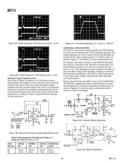
Figure 34. Buffer Recovery Time Source Current = 2 mA<br />
Figure 35. Buffer Recovery Time Sink Current = 1 mA<br />
Driving A Large Capacitive Load<br />
The circuit of Figure 36 employs a 100 Ω isolation resistor<br />
which enables the amplifier to drive capacitive loads exceeding<br />
1500 pF; the resistor effectively isolates the high frequency<br />
feedback from the load and stabilizes the circuit. <strong>Low</strong> frequency<br />
feedback is returned to the amplifier summing junction via the<br />
low pass filter formed by the 100 Ω series resistor and the load<br />
capacitance, C1. Figure 37 shows a typical transient response<br />
for this connection.<br />
Figure 37. Transient Response, R L = 2 kΩ, C L = 500 pF<br />
CMOS DAC APPLICATIONS<br />
The <strong>AD713</strong> is an excellent output amplifier for CMOS DACs.<br />
It can be used to perform both 2 and 4 quadrant operation. The<br />
output impedance of a DAC using an inverted R-2R ladder approaches<br />
R for codes containing many “1”s, 3R for codes containing<br />
a single “1” and infinity for codes containing all zeros.<br />
For example, the output resistance of the AD7545 will modulate<br />
between 11 kΩ and 33 kΩ. Therefore, with the DAC’s internal<br />
feedback resistance of 11 kΩ, the noise gain will vary<br />
from 2 to 4/3. This changing noise gain modulates the effect of<br />
the input offset voltage of the amplifier, resulting in nonlinear<br />
DAC amplifier performance. The <strong>AD713</strong>, with its guaranteed<br />
1.5 mV input offset voltage, minimizes this effect achieving<br />
12-bit performance.<br />
Figures 38 and 39 show the <strong>AD713</strong> and a 12-bit CMOS DAC,<br />
the AD7545, configured for either a unipolar binary (2-quadrant<br />
multiplication) or bipolar (4-quadrant multiplication) operation.<br />
Capacitor C1 provides phase compensation which<br />
reduces overshoot and ringing.<br />
Figure 38. Unipolar Binary <strong>Op</strong>eration<br />
Figure 36. Circuit for Driving a Large Capacitance Load<br />
Table II. Recommended Trim Resistor Values vs.<br />
Grades for AD7545 for V D = +5 V<br />
Trim JN/AQ/ KN/BQ/ LN/CQ/ GLN/GCQ/<br />
Resistor SD TD UD GUD<br />
R1 500 Ω 200 Ω 100 Ω 20 Ω<br />
R2 150 Ω 68 Ω 33 Ω 6.8 Ω<br />
Figure 39. Bipolar <strong>Op</strong>eration<br />
–10–<br />
REV. B


![Linear Collider [Accelerator] Overview](https://img.yumpu.com/33867705/1/190x143/linear-collider-accelerator-overview.jpg?quality=85)