AD713 Quad Precision, Low Cost, High Speed, BiFET Op Amp
AD713 Quad Precision, Low Cost, High Speed, BiFET Op Amp
AD713 Quad Precision, Low Cost, High Speed, BiFET Op Amp

Create successful ePaper yourself
Turn your PDF publications into a flip-book with our unique Google optimized e-Paper software.
a<br />
FEATURES<br />
Enhanced Replacement for LF347 and TL084<br />
AC PERFORMANCE<br />
1 s Settling to 0.01% for 10 V Step<br />
20 V/s Slew Rate<br />
0.0003% Total Harmonic Distortion (THD)<br />
4 MHz Unity Gain Bandwidth<br />
DC PERFORMANCE<br />
0.5 mV max Offset Voltage (<strong>AD713</strong>K)<br />
20 V/°C max Drift (<strong>AD713</strong>K)<br />
200 V/mV min <strong>Op</strong>en Loop Gain (<strong>AD713</strong>K)<br />
2 V p-p typ Noise, 0.1 Hz to 10 Hz<br />
True 14-Bit Accuracy<br />
Single Version: AD711, Dual Version: AD712<br />
Available in 16-Pin SOIC, 14-Pin Plastic DIP and<br />
Hermetic Cerdip Packages and in Chip Form<br />
MIL-STD-883B Processing Available<br />
Standard Military Drawing Available<br />
APPLICATIONS<br />
Active Filters<br />
<strong>Quad</strong> Output Buffers for 12- and 14-Bit DACs<br />
Input Buffers for <strong>Precision</strong> ADCs<br />
Photo Diode Preamplifier Applications<br />
PRODUCT DESCRIPTION<br />
The <strong>AD713</strong> is a quad operational amplifier, consisting of four<br />
AD711 <strong>BiFET</strong> op amps. These precision monolithic op amps<br />
offer excellent dc characteristics plus rapid settling times, high<br />
slew rates, and ample bandwidths. In addition, the <strong>AD713</strong> provides<br />
the close matching ac and dc characteristics inherent to<br />
amplifiers sharing the same monolithic die.<br />
The single-pole response of the <strong>AD713</strong> provides fast settling:<br />
l µs to 0.01%. This feature, combined with its high dc precision,<br />
makes it suitable for use as a buffer amplifier for 12- or 14-bit<br />
DACs and ADCs. It is also an excellent choice for use in active<br />
filters in 12-, 14- and 16-bit data acquisition systems. Furthermore,<br />
the <strong>AD713</strong>’s low total harmonic distortion (THD) level<br />
of 0.0003% and very close matching ac characteristics make it<br />
an ideal amplifier for many demanding audio applications.<br />
The <strong>AD713</strong> is internally compensated for stable operation at<br />
unity gain and is available in seven performance grades. The<br />
<strong>AD713</strong>J and <strong>AD713</strong>K are rated over the commercial temperature<br />
range of 0°C to +70°C. The <strong>AD713</strong>A and <strong>AD713</strong>B are<br />
rated over the industrial temperature of –40°C to +85°C. The<br />
<strong>AD713</strong>S and <strong>AD713</strong>T are rated over the military temperature<br />
range of –55°C to +125°C and are available processed to<br />
MIL-STD-883B, Rev. C.<br />
<strong>Quad</strong> <strong>Precision</strong>, <strong>Low</strong> <strong>Cost</strong>,<br />
<strong>High</strong> <strong>Speed</strong>, <strong>BiFET</strong> <strong>Op</strong> <strong>Amp</strong><br />
<strong>AD713</strong><br />
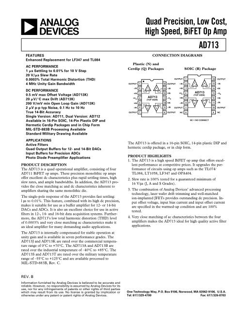
Plastic (N) and<br />
Cerdip (Q) Packages<br />
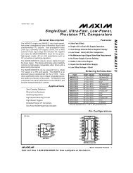
CONNECTION DIAGRAMS<br />
SOIC (R) Package<br />
OUTPUT 1<br />
14<br />
OUTPUT<br />
OUTPUT –IN<br />
1<br />
2 1 4<br />
16<br />
15<br />
OUTPUT<br />
–IN<br />
+IN 3<br />
12 +IN +V S<br />
4 <strong>AD713</strong> 13 –V S<br />
(TOP VIEW)<br />
+V S<br />
4 <strong>AD713</strong> 11 –V<br />
(TOP VIEW)<br />
S<br />
+IN 5<br />
12 +IN<br />
–IN 2 1 4 13 –IN +IN 3<br />
14 +IN<br />
+IN 5<br />
10 +IN –IN 6 2 3 11 –IN<br />
–IN 6<br />
2 3<br />
9 –IN OUTPUT 7<br />
10 OUTPUT<br />
OUTPUT 7 8 OUTPUT NC 8<br />
9 NC<br />
NC = NO CONNECT<br />
The <strong>AD713</strong> is offered in a 16-pin SOIC, 14-pin plastic DIP and<br />
hermetic cerdip package, or in chip form.<br />
PRODUCT HIGHLIGHTS<br />
1. The <strong>AD713</strong> is a high speed <strong>BiFET</strong> op amp that offers excellent<br />
performance at competitive prices. It upgrades the performance<br />
of circuits using op amps such as the TL074/<br />
TL084, LT1058, LF347 and OPA404.<br />
2. Slew rate is 100% tested for a guaranteed minimum of<br />
16 V/µs (J, A and S Grades).<br />
3. The combination of Analog Devices’ advanced processing<br />
technology, laser wafer drift trimming and well-matched<br />
ion-implanted JFETs provides outstanding dc precision. Input<br />
offset voltage, input bias current and input offset current<br />
are specified in the warmed-up condition and are 100%<br />
tested.<br />
4. Very close matching of ac characteristics between the four<br />
amplifiers makes the <strong>AD713</strong> ideal for high quality active filter<br />
applications.<br />
REV. B<br />
Information furnished by Analog Devices is believed to be accurate and<br />
reliable. However, no responsibility is assumed by Analog Devices for its<br />
use, nor for any infringements of patents or other rights of third parties<br />
which may result from its use. No license is granted by implication or<br />
otherwise under any patent or patent rights of Analog Devices.<br />
One Technology Way, P.O. Box 9106, Norwood, MA 02062-9106, U.S.A.<br />
Tel: 617/329-4700 Fax: 617/326-8703
<strong>AD713</strong>–SPECIFICATIONS (V S = 15 V @ T A = +25C unless otherwise noted)<br />
<strong>AD713</strong>J/A/S <strong>AD713</strong>K/B/T<br />
Parameter Conditions Min Typ Max Min Typ Max Units<br />
INPUT OFFSET VOLTAGE 1<br />
Initial Offset 0.3 1.5 0.2 0.5 mV<br />
Offset T MIN to T MAX 0.5 2/2/2 0.4 0.7/0.7/1.0 mV<br />
vs. Temp 5 5 20/20/15 µV/°C<br />
vs. Supply 78 95 84 100 dB<br />
vs. Supply T MIN to T MAX 76/76/76 95 84 100 dB<br />
Long-Term Stability 15 15 µV/Month<br />
INPUT BIAS CURRENT 2 V CM = 0 V 40 150 40 75 pA<br />
V CM = 0 V @ T MAX 3.4/9.6/154 1.7/4.8/77 nA<br />
V CM = ±10 V 55 200 55 120 pA<br />
INPUT OFFSET CURRENT V CM = 0 V 10 75 10 35 pA<br />
V CM = 0 V @ T MAX 1.7/4.8/77 0.8/2.2/36 nA<br />
MATCHING CHARACTERISTICS<br />
Input Offset Voltage 0.5 1.8 0.4 0.8 mV<br />
Input Offset Voltage T MIN to T MAX 0.7 2.3/2.3/2.3 0.6 1.0/1.0/1.3 mV<br />
Input Offset Voltage Drift 8 6 25 µV/°C<br />
Input Bias Current 10 100 10 35 pA<br />
Crosstalk f = 1 kHz –130 –130 dB<br />
f = 100 kHz –95 –95 dB<br />
FREQUENCY RESPONSE<br />
Small Signal Bandwidth Unity Gain 3.0 4.0 3.4 4.0 MHz<br />
Full Power Response V O = 20 V p-p 200 200 kHz<br />
Slew Rate Unity Gain 16 20 18 20 V/µs<br />
Settling Time to 0.01% 1.0 1.2 1.0 1.2 µs<br />
Total Harmonic Distortion f = 1 kHz; R L ≥ 2 kΩ; 0.0003 0.0003 %<br />
V O = 3 V rms<br />
INPUT IMPEDANCE<br />
Differential 3×10 12 5.5 3×10 12 5.5 ΩpF<br />
Common Mode 3×10 12 5.5 3×10 12 5.5 ΩpF<br />
INPUT VOLTAGE RANGE<br />
Differential 3 ±20 ±20 V<br />
Common-Mode Voltage 4 +14.5, –11.5 +14.5, –11.5 V<br />
T MIN to T MAX –11 +13 –11 +13 V<br />
Common Mode V CM = ±10 V 78 88 84 94 dB<br />
Rejection Ratio T MIN to T MAX 76/76/76 84 82 90 dB<br />
V CM = ±11 V 72 84 78 90 dB<br />
T MIN to T MAX 70/70/70 80 74 84 dB<br />
INPUT VOLTAGE NOISE 0.1 Hz to 10 Hz 2 2 µV p-p<br />
f = 10 Hz 45 45 nV/√Hz<br />
f = 100 Hz 22 22 nV/√Hz<br />
f = 1 kHz 18 18 nV/√Hz<br />
f = 10 kHz 16 16 nV/√Hz<br />
INPUT CURRENT NOISE f = 1 kHz 0.01 0.01 pA/√Hz<br />
OPEN-LOOP GAIN V O = ±10 V; R L ≥ 2 kΩ 150 400 200 400 V/mV<br />
T MIN to T MAX 100/100/100 100 V/mV<br />
OUTPUT CHARACTERISTICS<br />
Voltage R L ≥ 2 kΩ +13, –12.5 +13.9, –13.3 +13, –12.5 +13.9, –13.3 V<br />
T MIN to T MAX ± 12/±12/12 +13.8, –13.1 12 +13.8, –13.1 V<br />
Current Short Circuit 25 25 mA<br />
POWER SUPPLY<br />
Rated Performance ±15 ±15 V<br />
<strong>Op</strong>erating Range 4.5 18 4.5 18 V<br />
Quiescent Current 10.0 13.5 10.0 12.0 mA<br />
TRANSISTOR COUNT # of Transistors 120 120<br />
NOTES<br />
1 Input Offset Voltage specifications are guaranteed after 5 minutes of operation at T A = +25°C.<br />
2 Bias Current specifications are guaranteed maximum at either input after 5 minutes of operation at T A = +25°C. For higher temperatures, the current doubles every 10°C.<br />
3 Defined as voltage between inputs, such that neither exceeds ±10 V from ground.<br />
4 Typically exceeding –14.1 V negative common-mode voltage on either input results in an output phase reversal.<br />
Specifications subject to change without notice.<br />
–2–<br />
REV. B
<strong>AD713</strong><br />
ABSOLUTE MAXIMUM RATINGS 1, 2<br />
Supply Voltage . . . . . . . . . . . . . . . . . . . . . . . . . . . . . . . . . ±18 V<br />
Internal Power Dissipation 2<br />
Input Voltage 3 . . . . . . . . . . . . . . . . . . . . . . . . . . . . . . . . . ± 18 V<br />
Output Short Circuit Duration<br />
(For One <strong>Amp</strong>lifier) . . . . . . . . . . . . . . . . . . . . . . . . Indefinite<br />
Differential Input Voltage . . . . . . . . . . . . . . . . . . +V S and –V S<br />
Storage Temperature Range (Q) . . . . . . . . . . –65°C to +150°C<br />
Storage Temperature Range (N, R) . . . . . . . . –65°C to +125°C<br />
<strong>Op</strong>erating Temperature Range<br />
<strong>AD713</strong>J/K . . . . . . . . . . . . . . . . . . . . . . . . . . . . 0°C to +70°C<br />
<strong>AD713</strong>A/B . . . . . . . . . . . . . . . . . . . . . . . . . . –40°C to +85°C<br />
<strong>AD713</strong>S/T . . . . . . . . . . . . . . . . . . . . . . . . . –55°C to +125°C<br />
Lead Temperature Range (Soldering 60 sec) . . . . . . . . +300°C<br />
NOTES<br />
1 Stresses above those listed under “Absolute Maximum Ratings” may cause permanent<br />
damage to the device. This is a stress rating only and functional operation of<br />
the device at these or any other conditions above those indicated in the operational<br />
section of this specification is not implied. Exposure to absolute maximum rating<br />
conditions for extended periods may affect device reliability.<br />
2 Thermal Characteristics:<br />
14-Pin Plastic Package: θ JC = 30°C/Watt; θ JA = 100°C/Watt<br />
14-Pin Cerdip Package: θ JC = 30°C/Watt; θ JA = 110°C/Watt<br />
16-Pin SOIC Package: θ JC = 30°C/Watt; θ JA = 100°C/Watt<br />
3 For supply voltages less than ±18 V, the absolute maximum input voltage is equal<br />
to the supply voltage.<br />
ORDERING GUIDE<br />
Temperature Package Package<br />
Model Range Description <strong>Op</strong>tion*<br />
<strong>AD713</strong>AQ –40°C to +85°C 14-Pin Ceramic DIP Q-14<br />
<strong>AD713</strong>BQ –40°C to +85°C 14-Pin Ceramic DIP Q-14<br />
<strong>AD713</strong>JCHIPS 0°C to +70°C Bare Die<br />
<strong>AD713</strong>JN 0°C to +70°C 14-Pin Plastic DIP N-14<br />
<strong>AD713</strong>JR-16 0°C to +70°C 16-Pin Plastic SOIC R-16<br />
<strong>AD713</strong>JR-16-REEL 0°C to +70°C 16-Pin Plastic SOIC R-16<br />
<strong>AD713</strong>JR-16-REEL7 0°C to +70°C 16-Pin Plastic SOIC R-16<br />
<strong>AD713</strong>KN 0°C to +70°C 14-Pin Plastic DIP N-14<br />
<strong>AD713</strong>SCHIPS –55°C to +125°C Bare Die<br />
<strong>AD713</strong>SQ –55°C to +125°C 14-Pin Ceramic DIP Q-14<br />
<strong>AD713</strong>SQ/883B –55°C to +125°C 14-Pin Ceramic DIP Q-14<br />
<strong>AD713</strong>TQ –55°C to +125°C 14-Pin Ceramic DIP Q-14<br />
<strong>AD713</strong>TQ/883B –55°C to +125°C 14-Pin Ceramic DIP Q-14<br />
5962-9063301MCA –55°C to +125°C 14-Pin Ceramic DIP Q-14<br />
5962-9063302MCA –55°C to +125°C 14-Pin Ceramic DIP Q-14<br />
*N = Plastic DIP; Q = Cerdip; R = Small Outline IC (SOIC).<br />
METALIZATION PHOTOGRAPH<br />
Dimensions shown in inches and (mm).<br />
Contact factory for latest dimensions.<br />
REV. B –3–
<strong>AD713</strong>–Typical Characteristics<br />
Figure 1. Input Voltage Swing vs.<br />
Supply Voltage<br />
Figure 2. Output Voltage Swing vs.<br />
Supply Voltage<br />
Figure 3. Output Voltage Swing<br />
vs. Load Resistance<br />
Figure 4. Quiescent Current vs.<br />
Supply Voltage<br />
Figure 5. Input Bias Current vs.<br />
Temperature<br />
Figure 6. Output Impedance vs.<br />
Frequency, G = 1<br />
Figure 7. Input Bias Current vs.<br />
Common Mode Voltage<br />
Figure 8. Short Circuit Current<br />
Limit vs. Temperature<br />
Figure 9. Gain Bandwidth Product<br />
vs. Temperature<br />
–4–<br />
REV. B
<strong>AD713</strong><br />
Figure 10. <strong>Op</strong>en-Loop Gain and<br />
Phase Margin vs. Frequency<br />
Figure 11. <strong>Op</strong>en-Loop Gain vs.<br />
Supply Voltage<br />
Figure 12. Power Supply Rejection<br />
vs. Frequency<br />
Figure 13. Common Mode Rejection<br />
vs. Frequency<br />
Figure 14. Large Signal Frequency<br />
Response<br />
Figure 15. Output Swing and Error<br />
vs. Settling Time<br />
Figure 16. Total Harmonic Distortion<br />
vs. Frequency<br />
Figure 17. Input Noise Voltage<br />
Spectral Density<br />
Figure 18. Slew Rate vs. Input<br />
Error Signal<br />
REV. B –5–
<strong>AD713</strong><br />
Figure 19. Crosstalk Test Circuit<br />
Figure 20. Crosstalk vs. Frequency<br />
Figure 21a. Unity Gain Follower<br />
Figure 21b. Unity Gain Follower<br />
Pulse Response (Large Signal)<br />
Figure 21c. Unity Gain Follower<br />
Pulse Response (Small Signal)<br />
Figure 22a. Unity Gain Inverter<br />
Figure 22b. Unity Gain Inverter<br />
Pulse Response (Large Signal)<br />
Figure 22c. Unity Gain Inverter<br />
Pulse Response (Small Signal)<br />
–6–<br />
REV. B
<strong>AD713</strong><br />
MEASURING <strong>AD713</strong> SETTLING TIME<br />
The photos of Figures 24 and 25 show the dynamic response of<br />
the <strong>AD713</strong> while operating in the settling time test circuit of<br />
Figure 23. The input of the settling time fixture is driven by a<br />
flat-top pulse generator. The error signal output from the false<br />
summing node of A1, the <strong>AD713</strong> under test, is clamped, amplified<br />
by op amp A2 and then clamped again.<br />
The error signal is thus clamped twice: once to prevent overloading<br />
amplifier A2 and then a second time to avoid overloading<br />
the oscilloscope preamp. A Tektronix oscilloscope preamp<br />
type 7A26 was carefully chosen because it recovers from the approximately<br />
0.4 volt overload quickly enough to allow accurate<br />
measurement of the <strong>AD713</strong>’s 1 µs settling time. <strong>Amp</strong>lifier A2 is<br />
a very high speed FET input op amp; it provides a voltage gain<br />
of 10, amplifying the error signal output of the <strong>AD713</strong> under<br />
test (providing an overall gain of 5).<br />
Figure 25. Settling Characteristics to –10 V Step.<br />
Upper Trace: Output of <strong>AD713</strong> Under Test (5 V/div).<br />
<strong>Low</strong>er Trace: <strong>Amp</strong>lified Error Voltage (0.01%/ div)<br />
Figure 23. Settling Time Test Circuit<br />
POWER SUPPLY BYPASSING<br />
The power supply connections to the <strong>AD713</strong> must maintain a<br />
low impedance to ground over a bandwidth of 4 MHz or more.<br />
This is especially important when driving a significant resistive<br />
or capacitive load, since all current delivered to the load comes<br />
from the power supplies. Multiple high quality bypass capacitors<br />
are recommended for each power supply line in any critical application.<br />
A 0.1 µF ceramic and a 1 µF electrolytic capacitor as<br />
shown in Figure 26 placed as close as possible to the amplifier<br />
(with short lead lengths to power supply common) will assure<br />
adequate high frequency bypassing in most applications. A<br />
minimum bypass capacitance of 0.1 µF should be used for any<br />
application.<br />
Figure 24. Settling Characteristics 0 V to +10 V Step.<br />
Upper Trace: Output of <strong>AD713</strong> Under Test (5 V/div).<br />
<strong>Low</strong>er Trace: <strong>Amp</strong>lified Error Voltage (0.01%/div)<br />
Figure 26. Recommended Power Supply Bypassing<br />
REV. B –7–
<strong>AD713</strong><br />
A HIGH SPEED INSTRUMENTATION AMPLIFIER<br />
CIRCUIT<br />
The instrumentation amplifier circuit shown in Figure 27 can<br />
provide a range of gains from unity up to 1000 and higher using<br />
only a single <strong>AD713</strong>. The circuit bandwidth is 1.2 MHz at a<br />
gain of 1 and 250 kHz at a gain of 10; settling time for the entire<br />
circuit is less than 5 µs to within 0.01% for a 10 volt step,<br />
(G = 10). Other uses for amplifier A4 include an active data<br />
guard and an active sense input.<br />
A HIGH SPEED FOUR OP AMP CASCADED AMPLIFIER<br />
CIRCUIT<br />
Figure 29 shows how the four amplifiers of the <strong>AD713</strong> may be<br />
connected in cascade to form a high gain, high bandwidth amplifier.<br />
This gain of 100 amplifier has a –3 dB bandwidth greater<br />
than 600 kHz.<br />
Figure 29. A <strong>High</strong> <strong>Speed</strong> Four <strong>Op</strong> <strong>Amp</strong> Cascaded<br />
<strong>Amp</strong>lifier Circuit<br />
Figure 27. A <strong>High</strong> <strong>Speed</strong> Instrumentation <strong>Amp</strong>lifier Circuit<br />
Table I provides a performance summary for this circuit. The<br />
photo of Figure 28 shows the pulse response of this circuit for a<br />
gain of 10.<br />
Table I. Performance Summary for the <strong>High</strong> <strong>Speed</strong><br />
Instrumentation <strong>Amp</strong>lifier Circuit<br />
Gain R G Bandwidth T Settle (0.01%)<br />
1 NC 1.2 MHz 2 µs<br />
2 20 kΩ 1.0 MHz 2 µs<br />
10 4.04 kΩ 0.25 MHz 5 µs<br />
Figure 30. THD Test Circuit<br />
Figure 28. The Pulse Response of the <strong>High</strong> <strong>Speed</strong><br />
Instrumentation <strong>Amp</strong>lifier. Gain = 10<br />
HIGH SPEED OP AMP APPLICATIONS AND<br />
TECHNIQUES<br />
DAC Buffers (I-to-V Converters)<br />
The wide input dynamic range of JFET amplifiers makes them<br />
ideal for use in both waveform reconstruction and digital-audio<br />
DAC applications. The <strong>AD713</strong>, in conjunction with the AD1860<br />
DAC, can achieve 0.0016% THD (here at a 4fs or a 176.4 kHz<br />
update rate) without requiring the use of a deglitcher. Just such<br />
a circuit is shown in Figure 31. The 470 pF feedback capacitor<br />
used with IC2a, along with op amp IC2b and its associated<br />
components, together form a 3-pole low-pass filter. Each or all<br />
of these poles can be tailored for the desired attenuation and<br />
phase characteristics required for a particular application. In this<br />
application, one half of an <strong>AD713</strong> serves each channel in a twochannel<br />
stereo system.<br />
–8–<br />
REV. B
<strong>AD713</strong><br />
Figure 31. A D/A Converter Circuit for Digital Audio<br />
Figure 32. Harmonic Distortion as Frequency for the<br />
Digital Audio Circuit of Figure 31<br />
Driving the Analog Input of an A/D Converter<br />
An op amp driving the analog input of an A/D converter, such<br />
as that shown in Figure 33, must be capable of maintaining a<br />
constant output voltage under dynamically changing load conditions.<br />
In successive approximation converters, the input current<br />
is compared to a series of switched trial currents. The comparison<br />
point is diode clamped but may vary by several hundred<br />
millivolts, resulting in high frequency modulation of the A/D input<br />
current. The output impedance of a feedback amplifier is<br />
made artificially low by its loop gain. At high frequencies, where<br />
the loop gain is low, the amplifier output impedance can approach<br />
its open loop value.<br />
Figure 33. The <strong>AD713</strong> as an ADC Buffer<br />
Most IC amplifiers exhibit a minimum open loop output<br />
impedance of 25 Ω, due to current limiting resistors. A few<br />
hundred microamps reflected from the change in converter<br />
loading can introduce errors in instantaneous input voltage.<br />
If the A/D conversion speed is not excessive and the bandwidth<br />
of the amplifier is sufficient, the amplifier’s output<br />
will return to the nominal value before the converter makes<br />
its comparison. However, many amplifiers have relatively<br />
narrow bandwidths, yielding slow recovery from output<br />
transients. The <strong>AD713</strong> is ideally suited as a driver for A/D<br />
converters since it offers both a wide bandwidth and a high<br />
open loop gain.<br />
REV. B –9–
<strong>AD713</strong><br />
Figure 34. Buffer Recovery Time Source Current = 2 mA<br />
Figure 35. Buffer Recovery Time Sink Current = 1 mA<br />
Driving A Large Capacitive Load<br />
The circuit of Figure 36 employs a 100 Ω isolation resistor<br />
which enables the amplifier to drive capacitive loads exceeding<br />
1500 pF; the resistor effectively isolates the high frequency<br />
feedback from the load and stabilizes the circuit. <strong>Low</strong> frequency<br />
feedback is returned to the amplifier summing junction via the<br />
low pass filter formed by the 100 Ω series resistor and the load<br />
capacitance, C1. Figure 37 shows a typical transient response<br />
for this connection.<br />
Figure 37. Transient Response, R L = 2 kΩ, C L = 500 pF<br />
CMOS DAC APPLICATIONS<br />
The <strong>AD713</strong> is an excellent output amplifier for CMOS DACs.<br />
It can be used to perform both 2 and 4 quadrant operation. The<br />
output impedance of a DAC using an inverted R-2R ladder approaches<br />
R for codes containing many “1”s, 3R for codes containing<br />
a single “1” and infinity for codes containing all zeros.<br />
For example, the output resistance of the AD7545 will modulate<br />
between 11 kΩ and 33 kΩ. Therefore, with the DAC’s internal<br />
feedback resistance of 11 kΩ, the noise gain will vary<br />
from 2 to 4/3. This changing noise gain modulates the effect of<br />
the input offset voltage of the amplifier, resulting in nonlinear<br />
DAC amplifier performance. The <strong>AD713</strong>, with its guaranteed<br />
1.5 mV input offset voltage, minimizes this effect achieving<br />
12-bit performance.<br />
Figures 38 and 39 show the <strong>AD713</strong> and a 12-bit CMOS DAC,<br />
the AD7545, configured for either a unipolar binary (2-quadrant<br />
multiplication) or bipolar (4-quadrant multiplication) operation.<br />
Capacitor C1 provides phase compensation which<br />
reduces overshoot and ringing.<br />
Figure 38. Unipolar Binary <strong>Op</strong>eration<br />
Figure 36. Circuit for Driving a Large Capacitance Load<br />
Table II. Recommended Trim Resistor Values vs.<br />
Grades for AD7545 for V D = +5 V<br />
Trim JN/AQ/ KN/BQ/ LN/CQ/ GLN/GCQ/<br />
Resistor SD TD UD GUD<br />
R1 500 Ω 200 Ω 100 Ω 20 Ω<br />
R2 150 Ω 68 Ω 33 Ω 6.8 Ω<br />
Figure 39. Bipolar <strong>Op</strong>eration<br />
–10–<br />
REV. B
<strong>AD713</strong><br />
FILTER APPLICATIONS<br />
A Programmable State Variable Filter<br />
For the state variable or universal filter configuration of Figure<br />
40 to function properly, DACs A1 and B1 need to control the<br />
gain and Q of the filter characteristic, while DACs A2 and B2<br />
must accurately track for the simple expression of f C to be true.<br />
This is readily accomplished using two AD7528 DACs and one<br />
<strong>AD713</strong> quad op amp. Capacitor C3 compensates for the effects<br />
of op amp gain-bandwidth limitations.<br />
This filter provides low pass, high pass and band pass outputs<br />
and is ideally suited for applications where microprocessor control<br />
of filter parameters is required. The programmable range<br />
for component values shown is f C = 0 to 15 kHz and Q = 0.3<br />
to 4.5.<br />
GIC and FDNR FILTER APPLICATIONS<br />
The closely matched and uniform ac characteristics of the<br />
<strong>AD713</strong> make it ideal for use in GIC (gyrator) and FDNR (frequency<br />
dependent negative resistor) filter applications. Figures<br />
Figure 40. A Programmable State Variable Filter Circuit<br />
41 and 43 show the <strong>AD713</strong> used in two typical active filters.<br />
The first shows a single <strong>AD713</strong> simulating two coupled inductors<br />
configured as a one-third octave bandpass filter. A single<br />
section of this filter meets ANSI class II specifications and<br />
handles a 7.07 V rms signal with
<strong>AD713</strong><br />
If this is not practical, small lead capacitances (10–20 pF)<br />
should be added across R5 and R6. Figures 42 and 44 show the<br />
output amplitude vs. frequency of these filters.<br />
C1206a–5–11/90<br />
Figure 42. Output <strong>Amp</strong>litude vs. Frequency of 1/3<br />
Octave Filter<br />
Figure 44. Relative Output <strong>Amp</strong>litude vs. Frequency<br />
of Antialiasing Filter<br />
Figure 43. An Antialiasing Filter<br />
14-Pin Plastic (N-14A) DIP Package<br />
OUTLINE DIMENSIONS<br />
Dimensions shown in inches and (mm).<br />
14-Pin Cerdip (Q-14) Package<br />
16-Pin SOIC (R-16) Package<br />
PIN 1<br />
16 9<br />
1<br />
0.4133 (10.50)<br />
0.3977 (10.00)<br />
8<br />
0.2992 (7.60)<br />
0.2914 (7.40)<br />
0.4193 (10.65)<br />
0.3937 (10.00)<br />
0.1043 (2.65)<br />
0.0926 (2.35)<br />
PRINTED IN U.S.A.<br />
0.0118 (0.30)<br />
0.0040 (0.10)<br />
0.0500 (1.27)<br />
BSC<br />
0.0192 (0.49)<br />
0.0138 (0.35)<br />
0.0291 (0.74)<br />
0.0098 (0.25) x 45°<br />
0.0125 (0.32)<br />
0 0091 (0 23)<br />
8°<br />
0°<br />
0.0500 (1.27)<br />
0.0157 (0.40)<br />
–12–<br />
REV. B


![Linear Collider [Accelerator] Overview](https://img.yumpu.com/33867705/1/190x143/linear-collider-accelerator-overview.jpg?quality=85)