AD713 Quad Precision, Low Cost, High Speed, BiFET Op Amp
AD713 Quad Precision, Low Cost, High Speed, BiFET Op Amp
AD713 Quad Precision, Low Cost, High Speed, BiFET Op Amp

You also want an ePaper? Increase the reach of your titles
YUMPU automatically turns print PDFs into web optimized ePapers that Google loves.
<strong>AD713</strong><br />
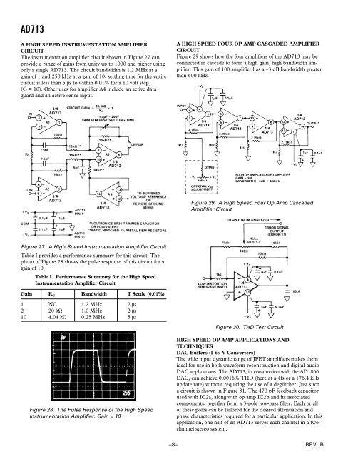
A HIGH SPEED INSTRUMENTATION AMPLIFIER<br />
CIRCUIT<br />
The instrumentation amplifier circuit shown in Figure 27 can<br />
provide a range of gains from unity up to 1000 and higher using<br />
only a single <strong>AD713</strong>. The circuit bandwidth is 1.2 MHz at a<br />
gain of 1 and 250 kHz at a gain of 10; settling time for the entire<br />
circuit is less than 5 µs to within 0.01% for a 10 volt step,<br />
(G = 10). Other uses for amplifier A4 include an active data<br />
guard and an active sense input.<br />
A HIGH SPEED FOUR OP AMP CASCADED AMPLIFIER<br />
CIRCUIT<br />
Figure 29 shows how the four amplifiers of the <strong>AD713</strong> may be<br />
connected in cascade to form a high gain, high bandwidth amplifier.<br />
This gain of 100 amplifier has a –3 dB bandwidth greater<br />
than 600 kHz.<br />
Figure 29. A <strong>High</strong> <strong>Speed</strong> Four <strong>Op</strong> <strong>Amp</strong> Cascaded<br />
<strong>Amp</strong>lifier Circuit<br />
Figure 27. A <strong>High</strong> <strong>Speed</strong> Instrumentation <strong>Amp</strong>lifier Circuit<br />
Table I provides a performance summary for this circuit. The<br />
photo of Figure 28 shows the pulse response of this circuit for a<br />
gain of 10.<br />
Table I. Performance Summary for the <strong>High</strong> <strong>Speed</strong><br />
Instrumentation <strong>Amp</strong>lifier Circuit<br />
Gain R G Bandwidth T Settle (0.01%)<br />
1 NC 1.2 MHz 2 µs<br />
2 20 kΩ 1.0 MHz 2 µs<br />
10 4.04 kΩ 0.25 MHz 5 µs<br />
Figure 30. THD Test Circuit<br />
Figure 28. The Pulse Response of the <strong>High</strong> <strong>Speed</strong><br />
Instrumentation <strong>Amp</strong>lifier. Gain = 10<br />
HIGH SPEED OP AMP APPLICATIONS AND<br />
TECHNIQUES<br />
DAC Buffers (I-to-V Converters)<br />
The wide input dynamic range of JFET amplifiers makes them<br />
ideal for use in both waveform reconstruction and digital-audio<br />
DAC applications. The <strong>AD713</strong>, in conjunction with the AD1860<br />
DAC, can achieve 0.0016% THD (here at a 4fs or a 176.4 kHz<br />
update rate) without requiring the use of a deglitcher. Just such<br />
a circuit is shown in Figure 31. The 470 pF feedback capacitor<br />
used with IC2a, along with op amp IC2b and its associated<br />
components, together form a 3-pole low-pass filter. Each or all<br />
of these poles can be tailored for the desired attenuation and<br />
phase characteristics required for a particular application. In this<br />
application, one half of an <strong>AD713</strong> serves each channel in a twochannel<br />
stereo system.<br />
–8–<br />
REV. B


![Linear Collider [Accelerator] Overview](https://img.yumpu.com/33867705/1/190x143/linear-collider-accelerator-overview.jpg?quality=85)