Square-like Silicon Crystal Rod Growth by FZ Method with ...
Square-like Silicon Crystal Rod Growth by FZ Method with ...
Square-like Silicon Crystal Rod Growth by FZ Method with ...

You also want an ePaper? Increase the reach of your titles
YUMPU automatically turns print PDFs into web optimized ePapers that Google loves.
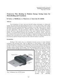
International Scientific Colloquium<br />
Modelling for Material Processing<br />
Riga, June 8-9, 2006<br />
<strong>Square</strong>-<strong>like</strong> <strong>Silicon</strong> <strong>Crystal</strong> <strong>Rod</strong> <strong>Growth</strong> <strong>by</strong> <strong>FZ</strong> <strong>Method</strong> <strong>with</strong><br />
Especially 3D Shaped HF Inductors<br />
A. Muiznieks, A. Rudevics, K. Lacis, H. Riemann, A. Lüdge, F.W. Schulze,<br />
B. Nacke<br />
Abstract<br />
The usage of square-<strong>like</strong> silicon crystals instead of circular shaped ones as a raw<br />
material for production of solar cells can reduce material loss and save processing steps of<br />
cutting round rods to the quadratic shape. Experimental work carried out <strong>by</strong> <strong>Silicon</strong> crystals<br />
group at Institute for <strong>Crystal</strong> <strong>Growth</strong> (Berlin, Germany) has shown for the first time that it is<br />
possible to grow squared silicon crystals <strong>by</strong> using specially shaped HF inductor in <strong>FZ</strong> method<br />
<strong>with</strong>out crystal rotation. To support the experimental work, a chain of mathematical models is<br />
created at Latvia University and is implemented in specialized software package Shape3D.<br />
This allows studying and analysing the features of the squared crystal growth process<br />
numerically.<br />
Introduction<br />
Today the solar cell technology has increasing significance as an alternative source of<br />
energy. Therefore the manufacturers of solar cells are interested to improve or optimize the<br />
process of cells production. One possible improvement is the usage of square-<strong>like</strong> silicon<br />
crystals instead of circular shaped ones as a raw material for solar cell production because the<br />
squared silicon crystals can reduce material loss and save processing steps of cutting round<br />
rods to the quadratic shape.<br />
The experimental work <strong>by</strong> <strong>Silicon</strong> crystals group at Institute for <strong>Crystal</strong> <strong>Growth</strong><br />
(Berlin, Germany) has shown that it is possible to grow square-<strong>like</strong> silicon crystals [1] <strong>by</strong><br />
using well known floating zone (<strong>FZ</strong>) method [2]. To achieve it, the crystal was not rotated and<br />
the heating was provided <strong>by</strong> specially designed 3D high frequency inductor. According to the<br />
literature, there were no attempts to grow four-cornered crystals <strong>by</strong> <strong>FZ</strong> method before.<br />
To support the experimental work, a chain of 3D mathematical models for crystal<br />
growth process in HF electromagnetic field is created at Latvia University and is implemented<br />
in specialized software package Shape3D. This allowed to study and analyse the features of<br />
the squared crystal growth process numerically.<br />
1. Short description of experiments of square-<strong>like</strong> silicon crystal growth <strong>by</strong> <strong>FZ</strong> method<br />
At first, the experiments at silicon crystal group of Institute for <strong>Crystal</strong> <strong>Growth</strong> were<br />
carried out to examine the behaviour of a conventional <strong>FZ</strong> crystal growth system after<br />
stopping the crystal rotation, see Fig. 1. In this case <strong>with</strong>out further measures, the local power<br />
maximum under the inductor main slit between current suppliers leads to a groove at the<br />
external phase boundary (3-phase line) resulting in outflow of the melt and, consequently, in<br />
the termination of the experiment.<br />
89
In the following experiments, the melt outflow was avoided <strong>by</strong> special measures<br />
starting <strong>with</strong> an inductor movement, immediately followed <strong>by</strong> reduction of the melt volume<br />
caused <strong>by</strong> the change of growing parameters. Again, grooving of the 3-phase line occurred,<br />
but to a lesser extent, and, surprisingly, in the majority of attempts the crystal continued to<br />
grow dislocation-free.<br />
The physical basis of the cross-section formation (Fig. 1) is the distribution of the<br />
induced high frequency (approx. 3 MHz) current density field on the silicon surfaces <strong>with</strong> the<br />
corresponding temperature field in the molten zone and <strong>with</strong> the adequate phase boundary<br />
shape. The formation of the four corners is the consequence of the local declines downwards<br />
of the 3-phase line. At the corners, the melt meniscus is pushed outwards <strong>by</strong> the locally<br />
increased static pressure acting against the surface tension pressure. Thus it appears that the<br />
crystal edges will be fewer rounds if the grooves of the 3-phase line get smaller and deeper.<br />
The Fig. 2 shows an example of the dislocation-free grown squared crystal rod <strong>with</strong><br />
rounded edges.<br />
Fig. 1. <strong>FZ</strong> crystal growth<br />
process <strong>with</strong>out crystal<br />
rotation, observed along a<br />
diagonal.<br />
Fig. 2. Dislocation-free<br />
grown <strong>FZ</strong> silicon crystal<br />
<strong>with</strong> square-<strong>like</strong> (diagonal<br />
ca.115 mm) cross-section,<br />
grown <strong>with</strong>out rotation.<br />
90
2. Mathematical modelling of the crystal growth process<br />
2.1. Principal scheme of mathematical modelling<br />
To model the four-cornered, i.e., square-<strong>like</strong> crystal growths process, first, the initial<br />
representation of crystal (e.g., round), feed rod and inductor must be created in 3D as shown<br />
in Fig. 3. Then the 3D boundary element method is used to calculate the high frequency<br />
electromagnetic field in the <strong>FZ</strong> system. The corresponding surface current lines on the silicon<br />
surfaces are shown in Fig. 4.<br />
Fig. 3. Initial representation of crystal, feed<br />
rod and inductor for EM calculations.<br />
Fig. 4. Calculated HF surface<br />
current density lines on the silicon<br />
surface, initial shape.<br />
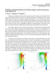
Due to the four slits in 3D inductor, the resulting maximums of electromagnetic power<br />
on the melt free surface are located below the ends of each slit as shown in Fig. 5. The main<br />
slit, i.e., the slit between the current suppliers has not real end but a special narrowing at the<br />
given distance from inductor centre. It is obviously that for growing of four-cornered crystals<br />
the inductors <strong>with</strong> 4 slits are needed.<br />
Fig. 5. Induced EM power density on<br />
the free surface <strong>with</strong> characteristic four<br />
maxima.<br />
Fig. 6. The square-<strong>like</strong> silicon crystal<br />
and melt free surface as the quasi-static<br />
solution <strong>with</strong> surface current lines.<br />
91
A special mathematical model accounts the influence of electromagnetic power on the<br />
shape of 3-phase line. As stated before at locations <strong>with</strong> higher electromagnetic power, the 3-<br />
phase line has groove downwards and therefore higher hydrostatic pressure there, which is<br />
compensated <strong>by</strong> higher curvature of free melt surface.<br />
For the calculation of the shape of melt free surface a special model is used, which<br />
considers the surface tension, hydrostatic pressure and electromagnetic pressure of the HF EM<br />
field.<br />
Iterative calculations <strong>with</strong> mentioned models lead to the formation of square-<strong>like</strong> shape<br />
of the growing crystal. In Fig. 6, an example of the quasi-static solution <strong>with</strong> the square-<strong>like</strong><br />
crystal and corresponding melt free surface is shown. The same solution from the bottom view<br />
is shown in Fig. 7.<br />
Fig. 7. The quasi-static solution for the shape of the crystal, bottom view.<br />
2.2. Specialized software package Shape3D<br />
Previously illustrated mathematical model for square-<strong>like</strong> crystal growth is<br />
implemented in the specialised software package Shape3D. The algorithm of calculations is<br />
illustrated in Fig. 8, where three calculation loops are emphasized.<br />
First loop (a) allows us to model the process of formation of square-<strong>like</strong> crystal <strong>with</strong><br />
assumption that the crystallization interface does not change in time. Loop (a) consists of 3D<br />
melt free surface calculation, followed <strong>by</strong> 3D electromagnetic field calculation and special<br />
algorithm for 3-phase line (i.e., external triple point line or ETP-Line) modification depending<br />
on the induced electromagnetic power.<br />
Next loop (b) enables us to take into account the temperature field inside the molten<br />
silicon and in the crystal. This allows a more precise modelling of the formation of fourcornered<br />
crystal. It involves the temperature field 3D calculation <strong>by</strong> boundary element method<br />
in the melt and the crystal. This calculation is coupled <strong>with</strong> module for radiation exchange<br />
calculation based on view factor approach.<br />
Finally, the loop (c) allows investigating of the shape of crystallization interface for a<br />
given 3-phase line.<br />
92
Fig. 8. Schematic depict of used calculation algorithm in program package Shape3D.<br />
Fig. 9. Displaying the 3D calculated temperature field on the melt free surface <strong>by</strong> Shape3D.<br />
The graphical user interface of Shape3D is shown in Fig. 9, where also an example of<br />
calculated temperature field distribution on the melt free surface is shown. An example of the<br />
<strong>by</strong> Shape3D 3D calculated shape of crystallization interface for the square-<strong>like</strong> crystal is<br />
shown in Fig. 10.<br />
93
Fig. 10. Vertical position of crystallization interface for I 0 = 700 A, V crcr = 1 mm/min,<br />
crystal height 50 mm.<br />
Conclusions<br />
The growth of square-shaped single silicon rods in <strong>FZ</strong> process <strong>with</strong>out crystal rotation<br />
is realized in Institute for <strong>Crystal</strong> <strong>Growth</strong> (Berlin, Germany). This opens new prospects of<br />
material development for cost-effective, high-efficiency solar cells. The supporting system of<br />
mathematical models and specialised program Shape3D are developed and have successfully<br />
contributed to the experiments.<br />
References<br />
[1] Annual Report 2004/05, Institute for <strong>Crystal</strong> <strong>Growth</strong>, Berlin, Germany. www.ikz-berlin.de<br />
[2] G. Ratnieks, A. Muiznieks, A. Mühlbauer. Modelling of phase boundaries for large industrial <strong>FZ</strong> silicon<br />
crystal growth <strong>with</strong> the needle-eye technique. J. <strong>Crystal</strong> <strong>Growth</strong>, Vol. 255 (2003), pp. 227-240.<br />
Authors<br />
Dr.-Phys. Muiznieks, Andris<br />
Ms.-comp. Rudevics, Andis<br />
Ms.-Phys. Lacis, Kaspars<br />
Faculty of Physics and Mathematics<br />
University of Latvia<br />
Zellu str. 8<br />
LV-1002 Riga, Latvia<br />
E-mail: andris.muiznieks@lu.lv<br />
Dr.-Phys. Riemann, Helge<br />
Dr.-Phys. Lüdge, Anke<br />
Institute for <strong>Crystal</strong> <strong>Growth</strong><br />
Max-Born-Str. 2<br />
D-12489 Berlin, Germany<br />
E-mail: riemann@ikz-berlin.de<br />
Prof., Dr.-Ing. Nacke, Bernard<br />
Institute for Eletctrothermal Processes<br />
University of Hanover<br />
Wilhelm-Busch Str. 4<br />
D-30167 Hanover, Germany<br />
E-mail: nacke@ewh.uni-hannover.de<br />
Schulze, Friedrich-Wilhelm<br />
PV <strong>Silicon</strong> AG<br />
Wilhelm-Wolff-Str. 25<br />
D-99099 Erfurt, Germany,<br />
E-mail:<br />
schulze@pvsilicon.com<br />
94