Mesoscopic thermal transport and energy dissipation in carbon ...
Mesoscopic thermal transport and energy dissipation in carbon ...
Mesoscopic thermal transport and energy dissipation in carbon ...

Create successful ePaper yourself
Turn your PDF publications into a flip-book with our unique Google optimized e-Paper software.
Physica B 323 (2002) 67–70<br />
<strong>Mesoscopic</strong> <strong>thermal</strong> <strong>transport</strong> <strong>and</strong> <strong>energy</strong> <strong>dissipation</strong><br />
<strong>in</strong> <strong>carbon</strong> nanotubes<br />
Philip Kim*,Li Shi,Arun Majumdar,Paul L. McEuen<br />
Department of Physics <strong>and</strong> Department of Mechanical Eng<strong>in</strong>eer<strong>in</strong>g, University of California Berkeley, CA 94720, USA<br />
Abstract<br />
We have measured the <strong>thermal</strong> conductivity of an <strong>in</strong>dividual multiwalled <strong>carbon</strong> nanotube (MWNT) us<strong>in</strong>g a<br />
microfabricated suspended device. The observed <strong>thermal</strong> conductivity is more than 3000 W/K-m at room temperature,<br />
which is two orders of magnitude higher than the estimation from previous experiments that used macroscopic mat<br />
samples. In addition,the temperature distributions <strong>in</strong> electrically heated MWNTs have been measured with a scann<strong>in</strong>g<br />
<strong>thermal</strong> microscope. The temperature profiles along the tube axis <strong>in</strong> MWNTs <strong>in</strong>dicate the bulk <strong>dissipation</strong> of electronic<br />
<strong>energy</strong> to phonons,which suggests diffusive electronic <strong>transport</strong>. r 2002 Elsevier Science B.V. All rights reserved.<br />
Keywords: <strong>Mesoscopic</strong> <strong>thermal</strong> <strong>transport</strong>; Thermal conductivity; Energy <strong>dissipation</strong>; Carbon nanotubes<br />
Carbon nanotubes are expected to have high<br />
<strong>thermal</strong> conductivity [1] <strong>and</strong> can conduct heat<br />
efficiently,thus prevent<strong>in</strong>g structure damage while<br />
used as current-carry<strong>in</strong>g wires <strong>in</strong> micro/nano<br />
devices. Previous electronic <strong>transport</strong> measurements<br />
at high electric field regime [2,3] suggested<br />
that <strong>carbon</strong> nanotubes can carry substantial<br />
amounts of current before their structural failure.<br />
To <strong>in</strong>vestigate these <strong>in</strong>trigu<strong>in</strong>g electrical <strong>and</strong><br />
<strong>thermal</strong> properties,mesoscopic experimental<br />
methods at a s<strong>in</strong>gle nanotube level are desirable.<br />
The <strong>thermal</strong> conductivity of <strong>carbon</strong> nanotubes<br />
have been measured by several groups us<strong>in</strong>g a<br />
millimeter sized mat sample [4–6]. Although these<br />
studies demonstrated qualitative underst<strong>and</strong><strong>in</strong>g of<br />
the low-dimensional nature of these materials,it is<br />
difficult to extract absolute values of the <strong>thermal</strong><br />
*Correspond<strong>in</strong>g author. Department of Physics,Columbia<br />
University,538 West 120th Street,New York,NY 10027,USA.<br />
Tel.: +1-212-854-0102; fax: +1-212-854-3379.<br />
E-mail address: pkim@phys.columbia.edu (P. Kim).<br />
conductivity <strong>in</strong> a mat sample due to the presence<br />
of numerous uncerta<strong>in</strong> tube–tube junctions that<br />
might be the dom<strong>in</strong>ant barriers to the <strong>thermal</strong><br />
<strong>transport</strong> through the sample.<br />
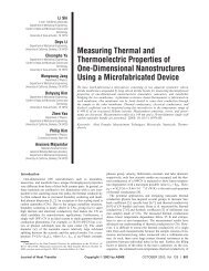
To perform mesoscopic <strong>thermal</strong> <strong>transport</strong> measurements,we<br />
have developed a microfabricated<br />
suspended device,hybridized with multiwalled<br />
nanotubes (MWNTs),to probe <strong>thermal</strong> <strong>transport</strong><br />
free from a substrate contact. Suspended structures<br />
were fabricated on a silicon nitride/silicon<br />
oxide/silicon multiplayer by pattern transfer <strong>and</strong><br />
electron beam lithography,followed by metalizations<br />
<strong>and</strong> etch<strong>in</strong>g processes. Fig. 1(a) shows a<br />
representative device <strong>in</strong>clud<strong>in</strong>g two 10 mm 10 mm<br />
adjacent silicon nitride membrane (0.5 mm thick)<br />
isl<strong>and</strong>s suspended with 200 mm long silicon nitride<br />
beams. On each isl<strong>and</strong>,a Pt th<strong>in</strong> film resistor,<br />
fabricated by electron beam lithography,serves as<br />
a heater to <strong>in</strong>crease the temperature of the<br />
suspended isl<strong>and</strong>. These resistors are electrically<br />
connected to contact pads by the metal l<strong>in</strong>es on the<br />
suspend<strong>in</strong>g legs. S<strong>in</strong>ce the resistance of the resistor<br />
0921-4526/02/$ - see front matter r 2002 Elsevier Science B.V. All rights reserved.<br />
PII: S 0921-4526(02)00969-9
68<br />
P. Kim et al. / Physica B 323 (2002) 67–70<br />
Fig. 1. SEM image of a suspended device to measure the <strong>thermal</strong> conductivity of an <strong>in</strong>dividual <strong>carbon</strong> nanotube. Inset represents an<br />
angled detail view of the central part of the device. A MWNT with the diameter of 14 nm bridges two suspended isl<strong>and</strong>s.<br />
changes with temperature,they also serve as a<br />
thermometer to measure the temperature of each<br />
isl<strong>and</strong>.<br />
A mechanical manipulation similar to that used<br />
for the fabrication of a nanotube scann<strong>in</strong>g probe<br />
microscopy tip was used to place MWNTs on the<br />
desired part of the device. This approach rout<strong>in</strong>ely<br />
produces a nanotube device that can be used to<br />
measure the <strong>thermal</strong> conductivity of the bridg<strong>in</strong>g<br />
nanotube segment. Shown <strong>in</strong> the <strong>in</strong>set of Fig. 1 is<br />
an example of such a device. An <strong>in</strong>dividual<br />
MWNT with a diameter of 14 nm forms a <strong>thermal</strong><br />
path between two suspended isl<strong>and</strong>s otherwise<br />
<strong>thermal</strong>ly isolated from each other. A bias voltage<br />
applied to one of the resistors, R h ; creates Joule<br />
heat, P; <strong>and</strong> <strong>in</strong>creases the temperature, T h ; of the<br />
heater isl<strong>and</strong> from the <strong>thermal</strong> bath temperature<br />
T 0 : In a steady state,there is a heat transfer to the<br />
other isl<strong>and</strong> through the nanotubes,<strong>and</strong> thus also<br />
the temperature, T s ; of the resistor R s rises. From<br />
the relation between T h <strong>and</strong> T s to P; we can<br />
estimate the <strong>thermal</strong> conductance of the MWNT<br />
[7].<br />
Shown <strong>in</strong> Fig. 2 is the result<strong>in</strong>g <strong>thermal</strong> conductivity<br />
of the <strong>in</strong>dividual MWNT <strong>in</strong> Fig. 1,after<br />
geometrical consideration of its diameter (14 nm)<br />
Fig. 2. The temperature dependent <strong>thermal</strong> conductivity of the<br />
MWNT <strong>in</strong> Fig. 1 (adapted from Ref. [7]).<br />
<strong>and</strong> length (2.5 mm). This result shows remarkable<br />
differences from the previous ‘bulk’ measurements.<br />
Most significantly,the room temperature<br />
value of the <strong>thermal</strong> conductivity is over 3000 W/<br />
K-m,whereas the previous ‘bulk’ measurement on<br />
a MWNT mat us<strong>in</strong>g the 3o method estimates only<br />
20 W/K-m [4]. Note that our observed value is also<br />
an order of magnitude higher than that of an<br />
aligned SWNT sample (250 W/K-m) [6],but
P. Kim et al. / Physica B 323 (2002) 67–70 69<br />
comparable to the recent theoretical expectation,<br />
6000 W/K-m [1]. This large difference between<br />
mesoscopic <strong>and</strong> ‘bulk’ measurements suggests that<br />
numerous highly resistive <strong>thermal</strong> junctions between<br />
the tubes largely dom<strong>in</strong>ate the <strong>thermal</strong><br />
<strong>transport</strong> <strong>in</strong> mat samples used <strong>in</strong> the previous<br />
study.<br />
In addition to the mesoscopic <strong>thermal</strong> conductivity<br />
measurement,we have measured the temperature<br />
distributions <strong>in</strong> electrically heated<br />
MWNTs with a scann<strong>in</strong>g <strong>thermal</strong> microscope.<br />
The nature of the electron <strong>transport</strong> <strong>in</strong> <strong>carbon</strong><br />
nanotubes is closely related to the <strong>energy</strong> <strong>dissipation</strong><br />
mechanism,<strong>and</strong> is often correlated with the<br />
temperature distribution along the tubes. Therefore,by<br />
measur<strong>in</strong>g the local temperature along the<br />
<strong>carbon</strong> nanotubes under electron <strong>transport</strong>,we<br />
should be able to correlate the nature of the<br />
electronic <strong>transport</strong> to the <strong>energy</strong> <strong>dissipation</strong><br />
mechanism.<br />
To probe the local temperature of MWNTs,<br />
<strong>thermal</strong> probe atomic force microscope (AFM)<br />
tips have been fabricated <strong>and</strong> used <strong>in</strong> our<br />
experiments [8]. The micro-patterned Pt <strong>and</strong> Cr<br />
l<strong>in</strong>es form a junction at the apex of the AFM tip<br />
that has a lateral topographic spatial resolution<br />
B30 nm <strong>and</strong> <strong>thermal</strong> spatial resolution B80 nm.<br />
Shown <strong>in</strong> Fig. 3 is the simultaneously taken<br />
topographic <strong>and</strong> correspond<strong>in</strong>g <strong>thermal</strong> signal,<br />
DT m ; on a 10 nm diameter MWNT device fabricated<br />
on 1 mm silicon oxide/silicon surface.<br />
Clearly, DT m is higher near the MWNT with the<br />
estimated tube temperature <strong>in</strong>crease B30 K at its<br />
highest position. The total electronic power<br />
dissipated <strong>in</strong> this device 22 mW along the length<br />
of the tube. This dissipated <strong>energy</strong> is transferred to<br />
the substrate eventually. S<strong>in</strong>ce the heat flow<br />
through the silicon oxide substrate is proportional<br />
to the temperature gradient,the power <strong>dissipation</strong><br />
through the substrate, Q; can be estimated from<br />
this image. The estimated Q is 8.5 mW,where the<br />
tube length LB4 mm. From this value,the junction<br />
<strong>thermal</strong> conductance per unit length of tube could<br />
be computed: K j ¼ Q=LðT t T s ÞB0:08 W/K-m<br />
where T t <strong>and</strong> T s is the tube <strong>and</strong> substrate<br />
temperature underneath of the tube,respectively.<br />
Fig. 3(c) shows the temperature map along the<br />
tube. This temperature profile exhibits a roughly<br />
Fig. 3. (a) Topographic image of a MWNT device. Scale bar<br />
represent 1 mm. (b) the correspond<strong>in</strong>g <strong>thermal</strong> signal simultaneously<br />
taken with (a). The applied bias voltage on the MWNT<br />
was 1 V <strong>and</strong> the current was 22 mA. (c) Temperature profile<br />
along the tube axis.<br />
parabolic temperature distribution along the tube<br />
length with a negative curvature. This temperature<br />
variation is <strong>in</strong>deed expected for a classical Ohmic<br />
conductor that has a f<strong>in</strong>ite bulk <strong>dissipation</strong> P<br />
<strong>in</strong>side the conductor. We also found that the tube<br />
temperature at the middle of the MWNT <strong>in</strong>creases<br />
quadratically as a function of the bias voltage V<br />
[9]. S<strong>in</strong>ce P ¼ V 2 =R for a dissipative Ohmic<br />
conductor where R is the resistance of the tube,<br />
these observations suggest that MWNTs are<br />
<strong>energy</strong> dissipative <strong>in</strong> the electron <strong>transport</strong> <strong>and</strong><br />
thus are a diffusive conductor.<br />
References<br />
[1] S. Berber,Y.K. Kwon,D. Tomanek,Phys. Rev. Lett. 84<br />
(2000) 4613.<br />
[2] Z. Yao,C.L. Kane,C. Dekker,Phys. Rev. Lett. 84 (2000)<br />
2941.<br />
[3] P. Coll<strong>in</strong>s,M. Hersam,M. Arnold,Ph. Avouris,Science 292<br />
(2001) 706.<br />
[4] W. Yi,L. Lu,A. Dian-l<strong>in</strong>,Z.W. Pan,S.S. Xie,Phys. Rev. B<br />
59 (1999) R9015.<br />
[5] J. Hone,M. Whitney,C. Piskoti,A. Zettl,Phys. Rev. B 59<br />
(1999) R2514.
70<br />
P. Kim et al. / Physica B 323 (2002) 67–70<br />
[6] J. Hone,M.C. Laguno,N.M. Nemes,A.T. Johnson,J.E.<br />
Fisher,D.A. Walters,M.J. Casavant,J. Schmidt,R.E.<br />
Smalley,Appl. Phys. Lett. 72 (2000) 666.<br />
[7] P. Kim,L. Shi,A. Majumdar,P.L. McEuen,Phys. Rev.<br />
Lett 87 (2001) 210522.<br />
[8] L. Shi,S. Plyasunov,A. Bachtold,P.L. McEuen,A.<br />
Majumdar,Appl. Phys. Lett. 77 (2000) 4295.<br />
[9] L. Shi,P. Kim,A. Bachtold,P.L. McEuen,A. Majumdar,<br />
unpublished.