Energy Band-Gap Engineering of Graphene Nanoribbons
Energy Band-Gap Engineering of Graphene Nanoribbons
Energy Band-Gap Engineering of Graphene Nanoribbons

Create successful ePaper yourself
Turn your PDF publications into a flip-book with our unique Google optimized e-Paper software.
PRL 98, 206805 (2007)<br />
PHYSICAL REVIEW LETTERS week ending<br />
18 MAY 2007<br />
<strong>Energy</strong> <strong>Band</strong>-<strong>Gap</strong> <strong>Engineering</strong> <strong>of</strong> <strong>Graphene</strong> <strong>Nanoribbons</strong><br />
Melinda Y. Han, 1 Barbaros Özyilmaz, 2 Yuanbo Zhang, 2 and Philip Kim 2<br />
1 Department <strong>of</strong> Applied Physics and Applied Mathematics, Columbia University, New York, New York 10027, USA<br />
2 Department <strong>of</strong> Physics, Columbia University, New York, New York 10027, USA<br />
(Received 21 February 2007; published 16 May 2007)<br />
We investigate electronic transport in lithographically patterned graphene ribbon structures where the<br />
lateral confinement <strong>of</strong> charge carriers creates an energy gap near the charge neutrality point. Individual<br />
graphene layers are contacted with metal electrodes and patterned into ribbons <strong>of</strong> varying widths and<br />
different crystallographic orientations. The temperature dependent conductance measurements show<br />
larger energy gaps opening for narrower ribbons. The sizes <strong>of</strong> these energy gaps are investigated by<br />
measuring the conductance in the nonlinear response regime at low temperatures. We find that the energy<br />
gap scales inversely with the ribbon width, thus demonstrating the ability to engineer the band gap <strong>of</strong><br />
graphene nanostructures by lithographic processes.<br />
DOI: 10.1103/PhysRevLett.98.206805 PACS numbers: 73.63. b, 73.22. f, 73.23. b<br />
The recent discovery <strong>of</strong> graphene [1], a single atomic<br />
sheet <strong>of</strong> graphite, has ignited intense research activities to<br />
elucidate the electronic properties <strong>of</strong> this novel twodimensional<br />
(2D) electronic system. Charge transport in<br />
graphene is substantially different from that <strong>of</strong> conventional<br />
2D electronic systems as a consequence <strong>of</strong> the linear<br />
energy dispersion relation near the charge neutrality point<br />
(Dirac point) in the electronic band structure [2,3]. This<br />
unique band structure is fundamentally responsible for<br />
the distinct electronic properties <strong>of</strong> carbon nanotubes<br />
(CNTs) [4].<br />
When graphene is patterned into a narrow ribbon, and<br />
the carriers are confined to a quasi-one-dimensional (1D)<br />
system, we expect the opening <strong>of</strong> an energy gap. Similar to<br />
CNTs, this energy gap depends on the width and crystallographic<br />
orientation <strong>of</strong> the graphene nanoribbon (GNR)<br />
[5,6]. However, despite numerous recent theoretical studies<br />
[7–15], the energy gap in GNRs has yet to be investigated<br />
experimentally.<br />
In this Letter, we present electronic transport measurements<br />
<strong>of</strong> lithographically patterned GNR structures where<br />
the lateral confinement <strong>of</strong> charge carriers creates an energy<br />
gap. More than two dozen GNRs <strong>of</strong> different widths and<br />
crystallographic orientations were measured. We find that<br />
the energy gap depends strongly on the width <strong>of</strong> the<br />
channel for GNRs in the same crystallographic direction,<br />
but no systematic crystallographic dependence is observed.<br />
The GNR devices discussed here are fabricated from<br />
single sheets <strong>of</strong> graphene which have been mechanically<br />
extracted from bulk graphite crystals onto a SiO 2 =Si substrate<br />
as described in Ref. [3]. <strong>Graphene</strong> sheets with lateral<br />
sizes <strong>of</strong> 20 m are contacted with Cr=Au (3=50 nm)<br />
metal electrodes. Negative tone e-beam resist, hydrogen<br />
silsesquioxane (HSQ), is then spun onto the samples and<br />
patterned to form an etch mask defining nanoribbons with<br />
widths ranging from 10–100 nm and lengths <strong>of</strong> 1–2 m.<br />
An oxygen plasma is introduced to etch away the unprotected<br />
graphene, leaving the GNR protected beneath the<br />
HSQ mask [Fig. 1(a)].<br />
In this Letter, we study two different types <strong>of</strong> device<br />
sets: device sets P1-P4 each contain many ribbons <strong>of</strong><br />
varying width running parallel [Fig. 1(b)], and a device<br />
sets D1 and D2 have ribbons <strong>of</strong> uniform width and varying<br />
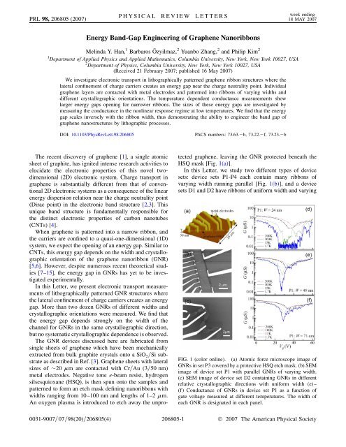
FIG. 1 (color online). (a) Atomic force microscope image <strong>of</strong><br />
GNRs in set P3 covered by a protective HSQ etch mask. (b) SEM<br />
image <strong>of</strong> device set P1 with parallel GNRs <strong>of</strong> varying width.<br />
(c) SEM image <strong>of</strong> device set D2 containing GNRs in different<br />
relative crystallographic directions with uniform width (e)–<br />
(f) Conductance <strong>of</strong> GNRs in device set P1 as a function <strong>of</strong><br />
gate voltage measured at different temperatures. The width <strong>of</strong><br />
each GNR is designated in each panel.<br />
0031-9007=07=98(20)=206805(4) 206805-1 © 2007 The American Physical Society
PRL 98, 206805 (2007)<br />
PHYSICAL REVIEW LETTERS week ending<br />
18 MAY 2007<br />
relative orientation [Fig. 1(c)]. In either case, each device<br />
within a given set is etched from the same sheet <strong>of</strong> graphene,<br />
so that the relative orientation <strong>of</strong> the GNRs within a<br />
given set is known.<br />
We remark that each GNR connects two blocks <strong>of</strong> wider<br />
( 0:5 m) graphene, which are in turn contacted by metal<br />
electrodes. Thus, unlike CNTs, Schottky barrier formation<br />
by the metal electrodes is absent in our GNR devices.<br />
Furthermore, multiple contacts on the wider block <strong>of</strong> graphene<br />
allow for four-terminal measurements in order to<br />
eliminate the residual contact resistance ( 1k ). A heavily<br />
doped silicon substrate below the 300 nm thick SiO 2<br />
dielectric layer serves as a gate electrode to tune the carrier<br />
density in the GNR. The width (W) and the length <strong>of</strong> each<br />
GNR were measured using a scanning electron microscope<br />
(SEM) after the transport measurements were performed.<br />
Since the HSQ protective layer was not removed from the<br />
GNR for this imaging, this measurement provides an upper<br />
bound to the true width <strong>of</strong> the GNR.<br />
The conductance G <strong>of</strong> the GNRs was measured using a<br />
standard lock-in technique with a small applied ac voltage<br />
( < 100 V@8 Hz). Figure 1(d)–1(f) shows the measured<br />
G <strong>of</strong> three representative GNR devices <strong>of</strong> varying width<br />
(W 24 4, 49 5, and 71 6nm) and uniform length<br />
(L 2 m) as a function <strong>of</strong> gate voltage V g at different<br />
temperatures. All curves exhibit a region <strong>of</strong> depressed G<br />
with respect to V g . In ‘‘bulk‘‘ (i.e., unpatterned) graphene,<br />
this dip in G is well understood and corresponds to the<br />
minimum conductivity 4e 2 =h at the charge neutrality<br />
point, V g V Dirac , where e and h are the electric charge<br />
and Planck constant, respectively. At room temperature,<br />
our GNRs exhibit qualitatively similar G V g behaviors,<br />
showing a minimum conductance G min on the order <strong>of</strong><br />
4e 2 =h W=L .<br />
Unlike the bulk case, GNRs with width W
PRL 98, 206805 (2007)<br />
PHYSICAL REVIEW LETTERS week ending<br />
18 MAY 2007<br />
We now discuss the quantitative scaling <strong>of</strong> the energy<br />
gap as a function <strong>of</strong> GNR width. By examining the differential<br />
conductance in the nonlinear response regime as a<br />
function <strong>of</strong> both the gate and bias voltage, we can directly<br />
measure the size <strong>of</strong> the energy gap [20]. Figure 3(a) shows<br />
a schematic energy band diagram for a GNR with source<br />
and drain electrodes. As the bias voltage, V b , increases, the<br />
source and drain levels approach the conduction and valence<br />
band edges, respectively. When conduction (valence)<br />
band edge falls into the bias window between the source<br />
and drain electrodes, electrons (holes) are injected from<br />
source (drain) and the current I rises sharply. The gate<br />
voltage adjusts the position <strong>of</strong> the gap relative to the<br />
source-drain levels. Figure 3(b)–3(d) shows the conductance<br />
versus V g and V b for three representative GNR<br />
devices <strong>of</strong> different width measured at T 1:6 K. The<br />
color indicates conductivity on a logarithmic scale, with<br />
the large dark area in each graph representing the turned<strong>of</strong>f<br />
region in the V g -V b plane where the both band edges are<br />
outside <strong>of</strong> the bias windows. The diamond shape <strong>of</strong> this<br />
region indicates that both V b and V g adjust the position <strong>of</strong><br />
the band edges relative to the source and drain energy<br />
levels, analogous to nonlinear transport in quantum dots<br />
[20]. As designated by the arrows, the GNR band gap E gap<br />
can be directly obtained from the value <strong>of</strong> V b at the vertex<br />
<strong>of</strong> the diamond.<br />
In order to obtain the quantitative scaling <strong>of</strong> E gap with<br />
respect to W, we now plot Egap 1 against W in Fig. 3(e) for a<br />
set <strong>of</strong> 13 parallel GNRs. The dashed line indicates a linear<br />
fit to the data, corresponding to E gap = W W ,<br />
where we obtained 0:2 eVnm and W 16 nm<br />
from the fit. Recent density functional theory studies<br />
[13,14] predict that the energy gap <strong>of</strong> a GNR scales inversely<br />
with the channel width, with a corresponding<br />
value ranging between 0:2–1:5 eVnm, which is consistent<br />
with this observation. We also note that W W 0 , in good<br />
agreement with the independent estimation <strong>of</strong> the GNR<br />
edge effects above.<br />
A similar scaling behavior holds even across GNR device<br />
sets running in different crystallographic directions<br />
[21]. Figure 4 shows the overall scaling <strong>of</strong> E gap as a<br />
function <strong>of</strong> W for six different device sets. Four device<br />
sets (P1–P4) have parallel GNRs with W ranging from 15–<br />
90 nm, and two device sets (D1, D2) have GNRs with<br />
similar W but different crystallographic directions. The<br />
energy gap behavior <strong>of</strong> all devices is well described by<br />
the scaling E gap = W W as discussed above, indicated<br />
by the dashed line. Remarkably, energy gaps as high<br />
as 200 meV are achieved by engineering GNRs as narrow<br />
as W 15 nm. Based on the empirical scaling determined<br />
here, a narrower GNR may show an even larger<br />
band gap, making the use <strong>of</strong> GNRs for semiconducting<br />
device components in ambient conditions a possibility.<br />
Finally, we remark on the crystallographic directional<br />
dependence <strong>of</strong> E gap . The inset to Fig. 4 shows E gap versus<br />
the relative orientation angle for two sets <strong>of</strong> GNRs. In<br />
principle, we expect E gap for each set to be periodic in ,<br />
provided all GNRs in the set have similar edge structures.<br />
However, experimental observation shows randomly scattered<br />
values around the average E gap corresponding to W<br />
FIG. 3 (color online). (a) Schematic<br />
energy band diagram <strong>of</strong> a GNR with<br />
bias voltage V b applied. The current I<br />
is controlled by both source-drain bias<br />
V b and gate voltage V g . (b)–(d) The<br />
differential conductance (dI=dV b ) <strong>of</strong><br />
three representative GNRs from set P4<br />
with W 22, 36, and 48 nm as a function<br />
<strong>of</strong> V b and V g measured at T<br />
1:6 K. The light (dark) color indicates<br />
high (low) conductance as designated by<br />
the color map. The horizontal arrows<br />
represent V b E gap =e. (e) Egap<br />
1 vs W<br />
obtained from similar analysis as (b)–<br />
(d), with a linear fit <strong>of</strong> the data.<br />
206805-3
PRL 98, 206805 (2007)<br />
PHYSICAL REVIEW LETTERS week ending<br />
18 MAY 2007<br />
Note added.—During the preparation <strong>of</strong> this manuscript<br />
we became aware <strong>of</strong> related work with a similar conclusion<br />
from Chen et al. [22].<br />
FIG. 4 (color online). E gap vs W for the 6 device sets considered<br />
in this study: four (P1–P4) <strong>of</strong> the parallel type and two (D1,<br />
D2) with varying orientation. The inset shows E gap vs relative<br />
angle for the device sets D1 and D2. Dashed lines in the inset<br />
show the value <strong>of</strong> E gap as predicted by the empirical scaling <strong>of</strong><br />
E gap vs W.<br />
with no sign <strong>of</strong> crystallographic directional dependence.<br />
This suggests that the detailed edge structure plays a more<br />
important role than the overall crystallographic direction in<br />
determining the properties <strong>of</strong> the GNRs. Indeed, theory for<br />
ideal GNRs predicts that E gap depends sensitively on the<br />
boundary conditions at the edges [6–15]. The lack <strong>of</strong><br />
directional dependence indicates that at this point our<br />
device fabrication process does not give us the atomically<br />
precise control <strong>of</strong> the GNR edges necessary to reveal this<br />
effect. The interplay between the precise width, edge orientation,<br />
edge structure, and chemical termination <strong>of</strong> the<br />
edges in GNRs remains a rich area for future research.<br />
In conclusion, we demonstrate that the energy gap in<br />
patterned graphene nanoribbons can be tuned during fabrication<br />
with the appropriate choice <strong>of</strong> ribbon width. An<br />
understanding <strong>of</strong> ribbon dimension and orientation as control<br />
parameters for the electrical properties <strong>of</strong> graphene<br />
structures can be seen as a first step toward the development<br />
<strong>of</strong> graphene-based electronic devices.<br />
We thank W. de Heer, C. T. White, F. Liu, S. G. Louie,<br />
M. Hybertsen, K. Bolotin, and P. Jarrillo-Herrero for helpful<br />
discussions. This work is supported by the ONR<br />
(No. N000150610138), FENA, DOE (No. DE-FG02-<br />
05ER46215), NSF CAREER (No. DMR-0349232),<br />
NSEC (No. CHE-0117752), and the New York State<br />
Office <strong>of</strong> Science, Technology, and Academic Research<br />
(NYSTAR). M. Han is supported by the National Science<br />
Foundation.<br />
[1] K. S. Novoselov et al., Science 306, 666 (2004).<br />
[2] K. S. Novoselov et al., Nature (London) 438, 197 (2005).<br />
[3] Y. Zhang, Y.-W. Tan, H. L. Stormer, and P. Kim, Nature<br />
(London) 438, 201 (2005).<br />
[4] M. S. Dresselhaus, G. Dresselhaus, and P. C. Eklund,<br />
Science <strong>of</strong> Fullerenes and Carbon Nanotubes<br />
(Academic, New York, 1996).<br />
[5] K. Nakada, M. Fujita, G. Dresselhaus, and M. S.<br />
Dresselhaus, Phys. Rev. B 54, 17 954 (1996).<br />
[6] K. Wakabayashi, M. Fujita, H. Ajiki, and M. Sigrist, Phys.<br />
Rev. B 59, 8271 (1999).<br />
[7] Y. Miyamoto, K. Nakada, and M. Fujita, Phys. Rev. B 59,<br />
9858 (1999).<br />
[8] M. Ezawa, Phys. Rev. B 73, 045432 (2006).<br />
[9] N. M. R. Peres, A. H. Castro Neto, and F. Guinea, Phys.<br />
Rev. B 73, 195411 (2006).<br />
[10] L. Brey and H. A. Fertig, Phys. Rev. B 73, 235411<br />
(2006).<br />
[11] Y. Ouyang, Y. Yoon, J. K. Fodor, and J. Guo, Appl. Phys.<br />
Lett. 89, 203107 (2006).<br />
[12] Y.-W. Son, M. L. Cohen, and S. G. Louie, Nature (London)<br />
444, 347 (2006).<br />
[13] Y.-W. Son, M. L. Cohen, and S. G. Louie, Phys. Rev. Lett.<br />
97, 216803 (2006).<br />
[14] V. Barone, O. Hod, and G. E. Scuseria, Nano Lett. 6, 2748<br />
(2006).<br />
[15] D. A. Areshkin, D. Gunlycke, and C. T. White, Nano Lett.<br />
7, 204 (2007).<br />
[16] Y.-W. Tan, Y. Zhang, H. L. Stormer, and P. Kim (unpublished).<br />
[17] The decreasing measured conductivity may originate from<br />
remnant contact contributions or the increase <strong>of</strong> inactive<br />
edge regions.<br />
[18] C. Berger et al., Science 312, 1191 (2006).<br />
[19] Because <strong>of</strong> difficulties in removing the HSQ etch mask<br />
and imaging the underlying ribbon without damage, we<br />
were able to measure the actual width <strong>of</strong> only a few GNRs<br />
studied in this experiment.<br />
[20] See, e.g. L. P. Kouwenhoven, C. M. Marcus, P. L. McEuen,<br />
S. Tarucha, R. M. Westervelt, and N. S. Wingreen, in<br />
Mesoscopic Electron Transport (Plenum, New York,<br />
1997).<br />
[21] Although the relative crystallographic directions between<br />
GNRs in a same graphene flake can be controlled by the<br />
proper lithography processes, the absolute crystallographic<br />
direction relative to the graphene lattice is unknown.<br />
[22] Z. Chen, Y. Lin, M. J. Rooks, and Ph. Avouris, cond-mat/<br />
0701599.<br />
206805-4