Energy Band-Gap Engineering of Graphene Nanoribbons
Energy Band-Gap Engineering of Graphene Nanoribbons
Energy Band-Gap Engineering of Graphene Nanoribbons

Create successful ePaper yourself
Turn your PDF publications into a flip-book with our unique Google optimized e-Paper software.
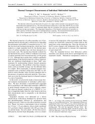
PRL 98, 206805 (2007)<br />
PHYSICAL REVIEW LETTERS week ending<br />
18 MAY 2007<br />
Note added.—During the preparation <strong>of</strong> this manuscript<br />
we became aware <strong>of</strong> related work with a similar conclusion<br />
from Chen et al. [22].<br />
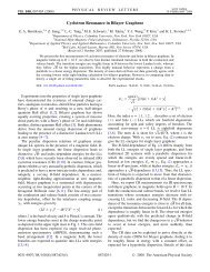
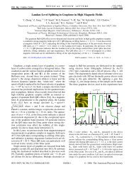
FIG. 4 (color online). E gap vs W for the 6 device sets considered<br />
in this study: four (P1–P4) <strong>of</strong> the parallel type and two (D1,<br />
D2) with varying orientation. The inset shows E gap vs relative<br />
angle for the device sets D1 and D2. Dashed lines in the inset<br />
show the value <strong>of</strong> E gap as predicted by the empirical scaling <strong>of</strong><br />
E gap vs W.<br />
with no sign <strong>of</strong> crystallographic directional dependence.<br />
This suggests that the detailed edge structure plays a more<br />
important role than the overall crystallographic direction in<br />
determining the properties <strong>of</strong> the GNRs. Indeed, theory for<br />
ideal GNRs predicts that E gap depends sensitively on the<br />
boundary conditions at the edges [6–15]. The lack <strong>of</strong><br />
directional dependence indicates that at this point our<br />
device fabrication process does not give us the atomically<br />
precise control <strong>of</strong> the GNR edges necessary to reveal this<br />
effect. The interplay between the precise width, edge orientation,<br />
edge structure, and chemical termination <strong>of</strong> the<br />
edges in GNRs remains a rich area for future research.<br />
In conclusion, we demonstrate that the energy gap in<br />
patterned graphene nanoribbons can be tuned during fabrication<br />
with the appropriate choice <strong>of</strong> ribbon width. An<br />
understanding <strong>of</strong> ribbon dimension and orientation as control<br />
parameters for the electrical properties <strong>of</strong> graphene<br />
structures can be seen as a first step toward the development<br />
<strong>of</strong> graphene-based electronic devices.<br />
We thank W. de Heer, C. T. White, F. Liu, S. G. Louie,<br />
M. Hybertsen, K. Bolotin, and P. Jarrillo-Herrero for helpful<br />
discussions. This work is supported by the ONR<br />
(No. N000150610138), FENA, DOE (No. DE-FG02-<br />
05ER46215), NSF CAREER (No. DMR-0349232),<br />
NSEC (No. CHE-0117752), and the New York State<br />
Office <strong>of</strong> Science, Technology, and Academic Research<br />
(NYSTAR). M. Han is supported by the National Science<br />
Foundation.<br />
[1] K. S. Novoselov et al., Science 306, 666 (2004).<br />
[2] K. S. Novoselov et al., Nature (London) 438, 197 (2005).<br />
[3] Y. Zhang, Y.-W. Tan, H. L. Stormer, and P. Kim, Nature<br />
(London) 438, 201 (2005).<br />
[4] M. S. Dresselhaus, G. Dresselhaus, and P. C. Eklund,<br />
Science <strong>of</strong> Fullerenes and Carbon Nanotubes<br />
(Academic, New York, 1996).<br />
[5] K. Nakada, M. Fujita, G. Dresselhaus, and M. S.<br />
Dresselhaus, Phys. Rev. B 54, 17 954 (1996).<br />
[6] K. Wakabayashi, M. Fujita, H. Ajiki, and M. Sigrist, Phys.<br />
Rev. B 59, 8271 (1999).<br />
[7] Y. Miyamoto, K. Nakada, and M. Fujita, Phys. Rev. B 59,<br />
9858 (1999).<br />
[8] M. Ezawa, Phys. Rev. B 73, 045432 (2006).<br />
[9] N. M. R. Peres, A. H. Castro Neto, and F. Guinea, Phys.<br />
Rev. B 73, 195411 (2006).<br />
[10] L. Brey and H. A. Fertig, Phys. Rev. B 73, 235411<br />
(2006).<br />
[11] Y. Ouyang, Y. Yoon, J. K. Fodor, and J. Guo, Appl. Phys.<br />
Lett. 89, 203107 (2006).<br />
[12] Y.-W. Son, M. L. Cohen, and S. G. Louie, Nature (London)<br />
444, 347 (2006).<br />
[13] Y.-W. Son, M. L. Cohen, and S. G. Louie, Phys. Rev. Lett.<br />
97, 216803 (2006).<br />
[14] V. Barone, O. Hod, and G. E. Scuseria, Nano Lett. 6, 2748<br />
(2006).<br />
[15] D. A. Areshkin, D. Gunlycke, and C. T. White, Nano Lett.<br />
7, 204 (2007).<br />
[16] Y.-W. Tan, Y. Zhang, H. L. Stormer, and P. Kim (unpublished).<br />
[17] The decreasing measured conductivity may originate from<br />
remnant contact contributions or the increase <strong>of</strong> inactive<br />
edge regions.<br />
[18] C. Berger et al., Science 312, 1191 (2006).<br />
[19] Because <strong>of</strong> difficulties in removing the HSQ etch mask<br />
and imaging the underlying ribbon without damage, we<br />
were able to measure the actual width <strong>of</strong> only a few GNRs<br />
studied in this experiment.<br />
[20] See, e.g. L. P. Kouwenhoven, C. M. Marcus, P. L. McEuen,<br />
S. Tarucha, R. M. Westervelt, and N. S. Wingreen, in<br />
Mesoscopic Electron Transport (Plenum, New York,<br />
1997).<br />
[21] Although the relative crystallographic directions between<br />
GNRs in a same graphene flake can be controlled by the<br />
proper lithography processes, the absolute crystallographic<br />
direction relative to the graphene lattice is unknown.<br />
[22] Z. Chen, Y. Lin, M. J. Rooks, and Ph. Avouris, cond-mat/<br />
0701599.<br />
206805-4