Energy Band-Gap Engineering of Graphene Nanoribbons
Energy Band-Gap Engineering of Graphene Nanoribbons
Energy Band-Gap Engineering of Graphene Nanoribbons

Create successful ePaper yourself
Turn your PDF publications into a flip-book with our unique Google optimized e-Paper software.
PRL 98, 206805 (2007)<br />
PHYSICAL REVIEW LETTERS week ending<br />
18 MAY 2007<br />
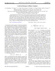
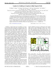
relative orientation [Fig. 1(c)]. In either case, each device<br />
within a given set is etched from the same sheet <strong>of</strong> graphene,<br />
so that the relative orientation <strong>of</strong> the GNRs within a<br />
given set is known.<br />
We remark that each GNR connects two blocks <strong>of</strong> wider<br />
( 0:5 m) graphene, which are in turn contacted by metal<br />
electrodes. Thus, unlike CNTs, Schottky barrier formation<br />
by the metal electrodes is absent in our GNR devices.<br />
Furthermore, multiple contacts on the wider block <strong>of</strong> graphene<br />
allow for four-terminal measurements in order to<br />
eliminate the residual contact resistance ( 1k ). A heavily<br />
doped silicon substrate below the 300 nm thick SiO 2<br />
dielectric layer serves as a gate electrode to tune the carrier<br />
density in the GNR. The width (W) and the length <strong>of</strong> each<br />
GNR were measured using a scanning electron microscope<br />
(SEM) after the transport measurements were performed.<br />
Since the HSQ protective layer was not removed from the<br />
GNR for this imaging, this measurement provides an upper<br />
bound to the true width <strong>of</strong> the GNR.<br />
The conductance G <strong>of</strong> the GNRs was measured using a<br />
standard lock-in technique with a small applied ac voltage<br />
( < 100 V@8 Hz). Figure 1(d)–1(f) shows the measured<br />
G <strong>of</strong> three representative GNR devices <strong>of</strong> varying width<br />
(W 24 4, 49 5, and 71 6nm) and uniform length<br />
(L 2 m) as a function <strong>of</strong> gate voltage V g at different<br />
temperatures. All curves exhibit a region <strong>of</strong> depressed G<br />
with respect to V g . In ‘‘bulk‘‘ (i.e., unpatterned) graphene,<br />
this dip in G is well understood and corresponds to the<br />
minimum conductivity 4e 2 =h at the charge neutrality<br />
point, V g V Dirac , where e and h are the electric charge<br />
and Planck constant, respectively. At room temperature,<br />
our GNRs exhibit qualitatively similar G V g behaviors,<br />
showing a minimum conductance G min on the order <strong>of</strong><br />
4e 2 =h W=L .<br />
Unlike the bulk case, GNRs with width W