Accurate Bit-Error-Rate Estimation for Efficient High Speed I/O Testing
Accurate Bit-Error-Rate Estimation for Efficient High Speed I/O Testing
Accurate Bit-Error-Rate Estimation for Efficient High Speed I/O Testing

Create successful ePaper yourself
Turn your PDF publications into a flip-book with our unique Google optimized e-Paper software.
<strong>Accurate</strong> <strong>Bit</strong>-<strong>Error</strong>-<strong>Rate</strong> <strong>Estimation</strong> <strong>for</strong> <strong>Efficient</strong> <strong>High</strong><br />
<strong>Speed</strong> I/O <strong>Testing</strong><br />
Dongwoo Hong and Kwang-Ting (Tim) Cheng<br />
Department of Electrical and Computer Engineering<br />
University of Cali<strong>for</strong>nia,<br />
Santa Barbara, CA 93106, USA<br />
besthdw@ece.ucsb.edu, timcheng@ece.ucsb.edu<br />
Abstract— We introduce a <strong>Bit</strong>-<strong>Error</strong>-<strong>Rate</strong> (BER) estimation<br />
technique <strong>for</strong> high-speed serial links, which utilizes the jitter<br />
spectral in<strong>for</strong>mation extracted from the transmitted data and<br />
some key characteristics of the clock and data recovery (CDR)<br />
circuit in the receiver. In addition to offering insight into both<br />
the behavior of the CDR loop and the contribution of the jitter<br />
to the BER, the estimation technique can be used to accelerate<br />
the jitter tolerance test by eliminating the conventional BER<br />
measurement process. We will discuss two different versions of<br />
the estimation technique: one <strong>for</strong> use with linear CDR circuits<br />
and the other <strong>for</strong> non-linear CDR circuits. Experimental results<br />
comparing the estimated BER and the measured BER<br />
demonstrate the high accuracy of the proposed technique.<br />
I. INTRODUCTION<br />
<strong>Bit</strong>-<strong>Error</strong>-<strong>Rate</strong> (BER) and jitter have been widely used as<br />
measurements to ensure the per<strong>for</strong>mance of high-speed<br />
communication systems. With the increasing number of I/O<br />
pins and greater data rates, testing high speed interfaces has<br />
posed significant challenges in terms of test cost and quality.<br />
Particularly, BER measurement down to the 10 -12 level, which<br />
is required to ensure system reliability <strong>for</strong> most multi-gigabit<br />
communication standards, is test-time prohibitive [1].<br />
In this paper, we propose a method <strong>for</strong> estimating the BER<br />
using the following two sets of parameters: (1) the jitter<br />
spectral in<strong>for</strong>mation, extracted from the signal at the input of<br />
the receiver. The in<strong>for</strong>mation includes the root-mean-square<br />
(rms) value of the random jitter (RJ) and the deterministic<br />
jitter (DJ) characteristics, such as frequencies and amplitudes<br />
of the periodic jitter (PJ) components. (2) The jitter transfer<br />
characteristics <strong>for</strong> both a linear CDR circuit and a non-linear<br />
CDR circuit.<br />
In the next section, we first summarize the jitter transfer<br />
characteristics of the CDR circuits. Section Ⅲ describes the<br />
BER estimation technique <strong>for</strong> the CDR circuits when both PJ<br />
and RJ are present in the data. Section Ⅳ presents the<br />
experimental results <strong>for</strong> the validation of the proposed<br />
technique. Section Ⅴ concludes the paper.<br />
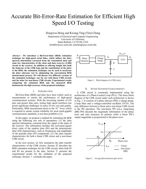
θ i<br />
Phase<br />
Detector<br />
Charge<br />
Pump<br />
Figure 1. Block diagram of a CDR circuit<br />
II. JITTER TRANSFER CHARATERISTICS<br />
A CDR circuit is commonly implemented using the<br />
architecture of a Phase-Locked Loop (PLL). The basic block<br />
diagram of the CDR circuit under such architecture is shown<br />
in Fig. 1. It consists of a phase detector (PD), a charge pump,<br />
a loop filter and a voltage-controlled oscillator (VCO). The<br />
only difference between a linear and a non-linear CDR circuit<br />
is the PD operation. The non-linear PD (a.k.a. bang-bang<br />
(BB) PD) discards the magnitude in<strong>for</strong>mation of the phase<br />
error and only measures its polarity while a linear PD’s<br />
output magnitude is proportional to the phase error.<br />
I P, avg<br />
I CP<br />
-θ th<br />
θ th Phase error<br />
-I CP<br />
Linear<br />
Non-linear<br />
(BB)<br />
Figure 2. Average phase dectector gain curves<br />
I P<br />
R<br />
C<br />
K VCO /s<br />
VCO<br />
θ o
Fig. 2 shows the characteristics of both the linear PD and<br />
the BB PD to the input jitter (i.e. phase error). The BB PD<br />
operates in the linear region <strong>for</strong> a small phase error whereas<br />
operates in the non-linear region <strong>for</strong> a large phase error. The<br />
average gain <strong>for</strong> the BB PD is smoothed by the metastability<br />
of flipflops in the PD and random jitter in the input data and<br />
the VCO, and, thus, has a finite slope across a narrow range<br />
of the phase error [2].<br />
θ in<br />
θ in,p<br />
θ<br />
t 0 t 1<br />
At a low jitter frequency, both PDs can track the input<br />
jitter closely, and thus no bit errors will occur. However, if<br />
the input jitter varies rapidly, the CDR circuits may not track<br />
the jitter, and some errors will occur. The responses to the<br />
high frequency jitters may be different from one another.<br />
θ out : Linear<br />
Δθ max<br />
θ out : Non-linear<br />
A. Linear CDR Circuit<br />
For the linear CDR circuit, if the jitter frequency is higher<br />
than the bandwidth of the CDR circuit, the recovered clock<br />
jitter has a certain delay and smaller amplitude compared to<br />
the injected one as shown in Fig. 3 [3].<br />
If we assume the input jitter as θ<br />
in<br />
= θin,p<br />
⋅sin(<br />
ωθt)<br />
, the<br />
recovered clock jitter can be represented as<br />
θout<br />
= θin,p<br />
θ<br />
⋅ H(jω)<br />
⋅sin(<br />
ω (t − τ(<br />
ω)))<br />
, where H( jω)<br />
is the close loop transfer function of the linear<br />
CDR circuit. The time-delay, τ, introduced into the recovered<br />
clock jitter depends on the phase response of the CDR circuit,<br />
and is represented as follows [4]:<br />
d<br />
τ ( ω)<br />
= − { ∠H( jω)}<br />
.<br />
dω<br />
There<strong>for</strong>e, the phase error which is the difference between the<br />
input jitter and the recovered clock jitter will be [3]:<br />
Δθ=<br />
θ<br />
2<br />
,p<br />
in<br />
2<br />
⋅( 1+<br />
H(jω)<br />
) −2⋅<br />
H(jω)<br />
⋅θin,p<br />
cos( ωθ<br />
⋅τ(<br />
ω))<br />
⋅sin(<br />
ωθt<br />
+ θ1)<br />
(1)<br />
where tanθ<br />
1<br />
= H(jω)<br />
⋅sin(<br />
ωθ τ(<br />
ω))/(1<br />
− H(jω)<br />
⋅cos(<br />
ωθτ(<br />
ω)))<br />
.<br />
B. Non-linear CDR Circuit<br />
For the non-linear CDR circuit, large and fast variation of<br />
the input jitter results in slewing because the available current<br />
beyond the linear region (i.e. I CP ) is constant [2]. Fig. 3<br />
illustrates an example of the slewing and the maximum phase<br />
error (i.e. Δθ max ) occurring at t 1 . The phase error at t 0 is used to<br />
approximate the maximum phase error because it is close<br />
enough to Δθ max and much simpler to calculate. If θ out slews<br />
<strong>for</strong> most of the period, t 0 is approximately equal to T θ /4 (T θ =<br />
2π/ω θ ). Denoting the input jitter as θin,p<br />
⋅sin(<br />
ωθ t + δ)<br />
, the<br />
maximum phase error could be approximated as:<br />
2 2 2 2<br />
4ωθθin , p<br />
− π K<br />
Δθ<br />
max<br />
≈ Δθ(t<br />
0<br />
) ==<br />
2ωθ<br />
The details of the derivation can be found in [2].<br />
2<br />
I<br />
2<br />
VCO P<br />
R<br />
2<br />
(2)<br />
Figure 3. Relationship between input jitter and recovered clock jitter<br />
III. BER ESTIMATION<br />
In the last section, we have shown the jitter transfer<br />
characteristics of the CDR loops with respect to the PJ. In the<br />
following, we discuss the BER estimation technique when<br />
both PJ and RJ components are present in the data.<br />
A. Linear CDR Circuit<br />
Since the CDR circuit can track only the low frequency<br />
components of the jitter, the rapidly varying RJ cannot be<br />
tracked. Fig. 4 shows the jitter in the transmitted data (i.e. total<br />
jitter = PJ + RJ), and the recovered clock jitter produced by<br />
the CDR circuit (from simulation). As expected, only PJ is<br />
tracked with a certain time delay and attenuated amplitude.<br />
There<strong>for</strong>e, the overall phase error becomes the summation of<br />
the phase error due to PJ (i.e. Equation (1)) and the RJ. <strong>Error</strong>s<br />
occur when the phase error exceeds plus or minus half of a<br />
Unit Interval T/2 (where T is denoted as one Unit Interval<br />
(UI)). That is, errors occur when<br />
θ<br />
in<br />
2<br />
,p<br />
2<br />
2<br />
T<br />
⋅( 1+<br />
H(jω)<br />
) −2⋅<br />
H(jω)<br />
⋅θin,p<br />
cos( ωθ<br />
⋅τ(<br />
ω))<br />
⋅sin(<br />
ωθt<br />
+θ1)<br />
+ n(t) ≥<br />
2<br />
where n(t) is the RJ.<br />
One popular approach to the BER estimation is the use of<br />
the double-delta model [5]. The model approximates the DJ as<br />
two Dirac delta functions and convolves them with the RJ. If<br />
we assume that the peak-to-peak magnitude of DJ as 2*A DJ<br />
and the rms value of RJ as σ<br />
RJ<br />
, the BER can be estimated as:<br />
T/ 2−<br />
ADJ<br />
BER = 2⋅ρT<br />
⋅Q(<br />
) . (3)<br />
σRJ<br />
The Q-function is used to calculate the probability that the<br />
Gaussian distribution is larger than any given value x, and is<br />
defined as:<br />
1 1 2<br />
−x<br />
/ 2<br />
Q (x) = [<br />
] e<br />
2<br />
( 1− a)x + a x + b 2π<br />
where a=1/π and b=2π [6]. In addition, the BER is linearly<br />
proportional to the transition density ( ρ ) of the data [5].<br />
T
Jitter (seconds)<br />
Recovered clock jitter<br />
– only PJ<br />
Recovered clock jitter<br />
– PJ+RJ<br />
Figure 4. Input jitter and recovered clock jitter <strong>for</strong> linear CDR circuit<br />
In our case, PJ and RJ are considered <strong>for</strong> the BER<br />
estimation. Since the PJ distribution cannot be properly<br />
modeled as two Dirac delta functions, we make some<br />
modifications to Equation (3). We use two new variables, the<br />
effective mean shifting (A eff ) and the effective rms value<br />
( σ eff ), to replace A DJ and σ RJ . Then, A eff and σ eff , to be<br />
applied to (3), will be:<br />
A<br />
2<br />
2<br />
2<br />
eff<br />
= θin,p<br />
⋅(1<br />
+ H(jω)<br />
) − 2⋅<br />
H(jω)<br />
⋅θin,p<br />
cos( ωθ<br />
⋅τ(<br />
ω))<br />
−0.9<br />
⋅ 2<br />
2<br />
eff = 1+<br />
0.84 )<br />
2<br />
RJ<br />
σ ( ⋅ σ .<br />
Number of samples<br />
⋅σ<br />
The details of the derivation of these two new variables, which<br />
are based on the ratio of the amount of RJ to the amount of PJ,<br />
can be found in [3].<br />
B. Non-linear CDR Circuit<br />
If the RJ is injected with PJ <strong>for</strong> the non-linear CDR<br />
circuit, the recovered clock jitter is affected by the RJ. When<br />
only PJ is present in the data, the recovered clock jitter<br />
increases monotonically during the first half of the jitter<br />
period as illustrated in Fig. 3. The peak-to-peak magnitude of<br />
the recovered clock jitter decreases linearly as the frequency<br />
of the PJ increases, which results in a -20dB/dec slope in the<br />
slewing region of the CDR’s jitter transfer function. However,<br />
in the presence of both PJ and RJ, the recovered clock jitter<br />
no longer increases monotonically. The peak-to-peak<br />
magnitude of the recovered clock jitter is less than that of the<br />
case in which only PJ is present, as shown in Fig. 5.<br />
There<strong>for</strong>e, the magnitude of the recovered clock jitter no<br />
longer decreases linearly in proportion to the increase in the<br />
jitter frequency. This results in a different slope in the<br />
slewing region <strong>for</strong> different PJ to RJ ratios. Because it is very<br />
difficult, if not impossible, to derive an analytical relationship<br />
between the slope variation and the jitter magnitude, we<br />
empirically derive their relationship from the simulation<br />
results as follows [7]:<br />
σ PJ 0.<br />
1<br />
−14.<br />
5 ⋅ ( ) − 5.<br />
5 + 0.<br />
5 ⋅ log2<br />
( )<br />
σ PJ + σ RJ<br />
σ RJ<br />
Slope =<br />
, if Slope > -18.5<br />
− 18.<br />
5<br />
, otherwise<br />
RJ<br />
Figure 5. Input jitter and recovered clock jitter <strong>for</strong> non-linear CDR circuit<br />
When only PJ is present in the data, the phase error<br />
distribution can be approximated using a Uni<strong>for</strong>m distribution<br />
with a peak-to-peak value of 2*Δθ max (Δθ max can be<br />
calculated from Equation (2)). This approximation correctly<br />
reflects the bounded property of the phase error distribution<br />
and is analytically convenient <strong>for</strong> BER estimation. When both<br />
RJ and PJ are present, the phase error distribution can be<br />
approximated by the convolution of a Uni<strong>for</strong>m and a<br />
Gaussian distribution because most of RJ components are not<br />
tracked by the CDR circuit. However, since the addition of<br />
the RJ changes the jitter transfer function of the CDR circuit,<br />
we need to modify Equation (2) <strong>for</strong> calculating the magnitude<br />
of the Uni<strong>for</strong>m distribution. To incorporate an increase in<br />
jitter magnitude due to the RJ, we simply substitute θ in,p in<br />
Equation (2) by θ in,TJ (θ in,TJ = θ in,p + σ RJ ). The total jitter<br />
magnitude is important <strong>for</strong> the non-linear CDR circuit<br />
because the jitter transfer function highly depends on the jitter<br />
magnitude. For the slope variation, we introduce a gain<br />
compensating factor that takes into account the gain<br />
difference in the slewing region, which is introduced by the<br />
addition of the RJ:<br />
Slope + 20<br />
⎛ w ⎞ 20<br />
⎜<br />
θ<br />
K slope (w θ ) = ⎟<br />
⎝ w −3dB<br />
⎠<br />
As a result, the maximum phase error becomes<br />
Δθ<br />
max_ TJ<br />
=<br />
4w<br />
2<br />
θ<br />
θ<br />
2<br />
in,TJ<br />
2w<br />
θ<br />
− π<br />
K<br />
2<br />
slope<br />
K<br />
2 2<br />
VCO<br />
(w<br />
I PR<br />
)<br />
Knowing the magnitude of the Uni<strong>for</strong>m distribution (i.e.<br />
Δθ max_TJ ) and the rms value of the Gaussian distribution (i.e.<br />
σ RJ ), the probability density function (PDF) of the phase error<br />
can be calculated by the convolution of these two<br />
distributions. In turn, the BER, which represents the<br />
probability that the phase error exceeds half of the UI, would<br />
be [7]:<br />
BER=1−<br />
1<br />
2A<br />
TJ<br />
1<br />
⋅<br />
2πσ<br />
RJ<br />
⎡ 05+ . A 2 2<br />
−t<br />
/ 2σ<br />
( 05+ . ATJ)<br />
+<br />
⎢⎣ ∫ e dt σ<br />
−∞<br />
0. 5−A<br />
2 2<br />
2 2<br />
TJ −t<br />
/ 2σRJ 2 −(<br />
05− . ATJ)<br />
/ 2σRJ<br />
−( 0.<br />
5−A<br />
−<br />
⎤<br />
TJ)<br />
∫ e dt σ<br />
−∞<br />
RJe<br />
(5)<br />
⎥⎦<br />
, where A TJ is the maximum phase error in UI (i.e. A TJ =<br />
Δθ max_TJ /(2π))<br />
θ<br />
2 2<br />
TJ RJ 2 −(<br />
05+ . ATJ)<br />
/ 2σRJ<br />
RJe<br />
2<br />
(4)
1.0E-07<br />
1.0E-08<br />
Mea. BER<br />
Est. BER<br />
1.0E-03<br />
1.0E-04<br />
BER<br />
1.0E-09<br />
1.0E-10<br />
1.0E-11<br />
BER<br />
1.0E-05<br />
1.0E-06<br />
1.0E-12<br />
0.01 0.1 1 10 100<br />
PJ Freq (MHz)<br />
1.0E-07<br />
4MHz 10MHz 15MHz 20MHz<br />
PJ Freq.<br />
Figure 6. BER measurement results <strong>for</strong> linear CDR circuit<br />
IV. EXPERIMENTAL RESULTS<br />
To validate the proposed estimation techniques, we<br />
conducted hardware measurements <strong>for</strong> the linear CDR circuit<br />
and simulations <strong>for</strong> the non-linear CDR circuit.<br />
A. Linear CDR circuit<br />
We conducted the experiments using the MAXIM 3873A<br />
CDR circuit, which operates at 2.488Gbps with 2MHz<br />
bandwidth and less than 0.1 dB jitter peaking [8]. We used<br />
Synthesys Research’s BERTScope <strong>for</strong> jitter injection and <strong>for</strong><br />
BER measurement. We injected PJ at 8 different frequencies,<br />
ranging from 50KHz to 80MHz with amplitude of 0.45UI.<br />
We fixed the rms value of RJ at 0.036UI, and swept the PJ’s<br />
frequency. In the low frequency range, the expected BER is<br />
too low to be measured (i.e. less than 10 -12 ) within a<br />
reasonable amount of time due to the CDR circuit’s tracking<br />
ability. Thus, if no error is captured within a time limit (in our<br />
experiment, the limit was set to 7 minutes≈ 10 12 b/(2.5Gb/s)),<br />
the BER is represented as 10 -12 as in Fig. 6. For these cases,<br />
the estimated BER is indeed much lower than 10 -12 . The<br />
results clearly show that the measured BER and the estimated<br />
BER match very well in almost all cases. When the measured<br />
BER level is around 10 -12 , the difference is larger than those<br />
of other cases. We suspect that this is because the injected RJ<br />
does not have the unbounded tails in real applications – thus<br />
the Gaussian model <strong>for</strong> the RJ may not accurate in the very<br />
low probability region.<br />
B. Non-inear CDR circuit<br />
We conducted MATLAB simulations to validate the BER<br />
estimation technique <strong>for</strong> the non-linear CDR circuit. The<br />
behavioral model of the CDR circuit operating at 10 Gb/s was<br />
used <strong>for</strong> the validation. Due to the limited simulation time,<br />
we could only af<strong>for</strong>d to conduct simulations down to the 10 -7<br />
BER level. For each case, we conducted the simulation to the<br />
point at which 1,000 errors were captured. The rms value of<br />
RJ was chosen at 0.1UI and the peak-to-peak PJ magnitude<br />
was chosen at 0.4UI. We injected four different PJ<br />
frequencies <strong>for</strong> the simulation. Fig. 7 shows the simulation<br />
results.<br />
Est. BER w/o comp. Est. BER w/ comp. Sim. BER<br />
Figure 7. BER simulation results <strong>for</strong> non-linear CDR circuit<br />
The graph contains the simulated BER and two estimated<br />
BERs: one is the estimated BER without compensating the<br />
jitter transfer variations due to the RJ (i.e. Substituting<br />
Equation (2) into Equation (5)) and the other is the estimated<br />
BER with compensation of these effects (i.e. Substituting<br />
Equation (4) into Equation (5)). The simulation results<br />
indicate that the simulated BER and the estimated BER, after<br />
compensating the jitter transfer variations, match pretty well.<br />
V. CONCLUSION<br />
<strong>High</strong> per<strong>for</strong>mance serial communication systems often<br />
require the BER to be at levels of 10 -12 or below. The<br />
excessive testing time <strong>for</strong> measuring such a low BER is a<br />
major hindrance <strong>for</strong> cost effective testing. Thus, the industry<br />
demands new testing methods that are both efficient and<br />
accurate to guarantee that products meet the BER specification<br />
at a low test cost. In this paper, we show how the PJ and RJ<br />
affect the recovered clock jitter and the dependency of the<br />
BER on the characteristics of the CDR circuit. We further<br />
propose an analytical technique to estimate the BER. The<br />
experimental results demonstrate the validity of our analysis<br />
and the roles of these parameters in determining the BER.<br />
REFERENCES<br />
[1] Y. Cai et al, “Digital Serial Communication Device <strong>Testing</strong> and Its<br />
Implication on Automatic Test Equipment Architecture,” IEEE Proc. of<br />
International Test Conference, pp 600-609, Oct. 2002.<br />
[2] J. Lee et al., “Analysis and Modeling of Bang-Bang Clock and Data<br />
Recovery Circuits,” ” IEEE Journal of Solid State Circuits, Vol. 39,<br />
No. 9, pp. 1571-1580, Sep. 2004.<br />
[3] D. Hong et al., “<strong>Bit</strong> <strong>Error</strong> <strong>Rate</strong> <strong>Estimation</strong> <strong>for</strong> <strong>High</strong> <strong>Speed</strong> Serial<br />
Links,” IEEE Transaction on Circuits and Systems Ⅰ, Vol. 53, No. 12,<br />
pp. 2616-2627, Dec. 2006.<br />
[4] A. V. Oppenheim and A.S. Willsky, Signals and Systems, Prentice Hall,<br />
1983.<br />
[5] Agilent Technologies, Jitter Analysis: The dual-Dirac Model, RJ/DJ,<br />
and Q-Scale, White Paper, Available at www.agilent.com.<br />
[6] A. Leon-Garcia, Probability and Random Processes <strong>for</strong> Electrical<br />
Engineering. Addison Wesley, 1994.<br />
[7] D. Hong et al., “<strong>Bit</strong>-<strong>Error</strong> <strong>Rate</strong> <strong>Estimation</strong> <strong>for</strong> Bang-Bang Clock and<br />
Data Recovery Circuit in <strong>High</strong>-<strong>Speed</strong> Serial Links,” IEEE Proc. of<br />
VLSI Test Symposium, pp. 17-22, Apr. 2008.<br />
[8] Maxim Integrated Products, Low-Power, Compact 2.5Gbps/2.7Gbps<br />
Clock-Recovery and Data-Retiming IC, Available at www.maximic.com.