The Micronic Mydata LDI 5s Series
The Micronic Mydata LDI 5s Series
The Micronic Mydata LDI 5s Series

Create successful ePaper yourself
Turn your PDF publications into a flip-book with our unique Google optimized e-Paper software.
<strong>The</strong> <strong>Micronic</strong> <strong>Mydata</strong> <strong>LDI</strong> <strong>5s</strong> <strong>Series</strong><br />
Providing a competitive edge to IC substrate makers
Laser direct imaging with the<br />
highest precision and productivity<br />
in the industry<br />
<strong>The</strong> <strong>Micronic</strong> <strong>Mydata</strong> <strong>LDI</strong> <strong>5s</strong> <strong>Series</strong> builds on the<br />
company’s core competencies including large area<br />
patterning, gray scale SLM technology, UV lasers,<br />
high-speed data handling and precision mechanics.<br />
<strong>The</strong>se are combined with an innovative scanning<br />
system and twin tables, resulting in a system that<br />
delivers high resolution and pattern placement<br />
accuracy without compromising productivity<br />
Sub-10μm resolution<br />
<strong>The</strong> optical system projects sharp sub-10μm images<br />
in dry film resist, yielding vertical profiles for<br />
accurate copper plating. A proprietary linear gray<br />
scale spatial light modulator (SLM) generates a fine<br />
writing grid for precise positioning of pattern features.<br />
L/S=7/7µm (Pitch 14µm),<br />
7µm lines 19µm and spaces thick dry in 19μm film resist dry film (DFR) resist (DFR)<br />
Unmatched productivity and precision<br />
<strong>The</strong> revolutionary optical projection system provides<br />
smooth and efficient rotor-based scanning.<br />
Four writing arms scan the panel in turn, minimizing<br />
overhead time. <strong>The</strong> <strong>Micronic</strong> <strong>Mydata</strong> <strong>LDI</strong> <strong>5s</strong> <strong>Series</strong><br />
can be integrated into packaging production lines<br />
using industry standard mechanical and electrical<br />
interfaces. It features a high-speed material handler<br />
that supports unmatched productivity and precision.
Autofocus system<br />
Actively follows the substrate topography<br />
for optimal focus performance<br />
Sub-10μm alignment<br />
Accurate alignment and pattern overlay are achieved<br />
by mapping the pattern data to match any distortions<br />
and irregularities of the individual panels. This<br />
is done in real time for each panel by measuring the<br />
alignment mark positions with the three widefield<br />
alignment cameras. A high-speed graphics processor-based<br />
datapath adapts the pattern to each panel<br />
without sacrificing productivity.<br />
Load panel<br />
Measure<br />
alignment<br />
Procedure to test alignment overlay<br />
Load panel<br />
Expose layer 1 Expose layer 2<br />
Unload panel<br />
Measure<br />
alignment<br />
Unload panel<br />
Develop panel<br />
Measure<br />
panel<br />
High throughput<br />
A high-power, 355nm diode-pumped solid state<br />
laser allows for the use of conventional dry film<br />
resists, on panel sizes of up to 510 x 515mm 2 .<br />
<strong>The</strong> high productivity provided by the <strong>Micronic</strong><br />
<strong>Mydata</strong> <strong>LDI</strong> <strong>5s</strong> <strong>Series</strong> is largely enabled by an<br />
innovative twin-stage design. As a panel is being<br />
printed on one of the stages, the next panel is<br />
loaded onto the other stage where alignment and<br />
focus mapping are performed. Thus writing and<br />
alignment are done in parallel so that throughput is<br />
not sacrificed. <strong>The</strong> stages then swap positions and<br />
continue to alternate without interruption, meaning<br />
that the tool effectively writes continuously.<br />
Twin table stage system<br />
Allows concurrent writing and<br />
substrate align/load/unload<br />
Alignment overlay data<br />
distribution showing 4<br />
performance of 2.5µm<br />
Deviation from first layer:<br />
Mean = 1.1µm, 4σ = 2.5µm, Max = 3.6µm<br />
Alignment overlay test grid<br />
Scale = 10µm per grid point<br />
(465 x 465 mm array)<br />
Position deviation from first layer<br />
scale=10µm/grid, area 465*465 mm<br />
X-deviation Y-deviation from first layer layer [µm][μm]<br />
10 µm<br />
5 µm<br />
Y-deviation X-deviation from first layer [µm] [μm]
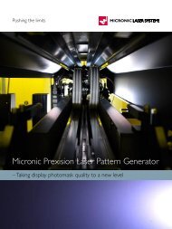
Pushing the limits<br />
<strong>Micronic</strong> <strong>Mydata</strong> worldwide<br />
HEADQUARTERS<br />
<strong>Micronic</strong> <strong>Mydata</strong> AB<br />
PO Box 3141<br />
SE-183 03 Täby<br />
Sweden<br />
Tel: +46 8 638 52 00<br />
Fax: +46 8 638 52 90<br />
Visit: Nytorpsvägen 9, Täby<br />
info@micronic-mydata.com<br />
CHINA<br />
<strong>Micronic</strong> <strong>Mydata</strong> (Shanghai) Co., Ltd.<br />
Unit 101, K Block<br />
Lane 168, Da Duhe Road.<br />
Putuo District, 200062<br />
Shanghai P.R. China<br />
Tel: +86 21 3252 3785/86<br />
Fax: +86 21 3252 3780<br />
JAPAN<br />
<strong>Micronic</strong> <strong>Mydata</strong> Japan K.K.<br />
Mitsugi-Kotobukicho Bldg.<br />
1-1-3 Kotobuki-cho<br />
Fuchu-shi<br />
Tokyo 183-0056<br />
Tel: +81 42-354-1320<br />
Fax:+81 42-354-1321<br />
SOUTH KOREA<br />
<strong>Micronic</strong> Laser Systems Korea Co Ltd<br />
3rd Floor Jung-San<br />
Bldg. 1026-8<br />
Sanbon-Dong, Gunpo-Si<br />
Gyeonggi-Do, 435-040<br />
Tel: +82-31-387-5111<br />
Fax: +82-31-388-0087<br />
TAIWAN<br />
<strong>Micronic</strong> Laser Systems/ Hermes-Epitek Corp<br />
Second Floor<br />
#18 Pu-Ding Road<br />
Der-An building<br />
Hsin-Chu, 300<br />
Tel: +886-3-564-6656<br />
Fax: +886-3-564-6664<br />
USA<br />
<strong>Micronic</strong> Laser Systems Inc.<br />
1922 Zanker Road<br />
San Jose<br />
CA 95112<br />
Tel: +1 (408) 392 2260<br />
Fax:+1 (408) 392 2261<br />
<strong>Micronic</strong> <strong>Mydata</strong> patents:<br />
US 7 710 634, US 7 715 641, US 7 787 174, US 7 800 815, US 7 842 926, US 2010/0225974 A1, US 2010/0208329 A1, US 2010/0142838 A1, US 2010/0229146 A1, US 2010/0225943, A1, US 2010/0225236 A1, US 2010/0141966 A1,<br />
US 2010/0142757 A1, US 2010/0225992 A1, US 2010/0225979 A1, WO 2010/100270 A1, WO 2010/100273 A2, WO 2010/063830, A1, WO 2010/063826 A1, WO 2010/063827 A1, WO 2010/100272 A1, WO 2010/100268 A2,<br />
WO 2010/092188 A1, WO 2010/092189 A1, WO 2010/100269 A1, WO 2010/092128 A1, other patents pending.<br />
<strong>Micronic</strong> <strong>Mydata</strong> AB (publ.), Nytorpsvägen 9, Box 3141, 183 03 Täby, Sweden. Tel +46 8 638 52 00. Fax +46 8 638 52 90 www.micronic-mydata.com<br />
AB16791 Oct 2011