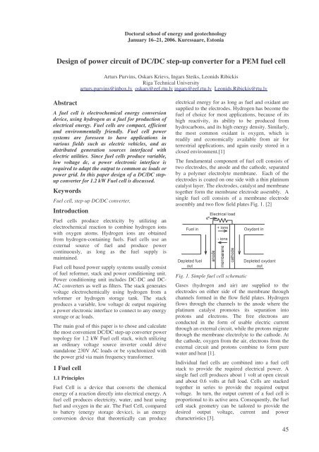
Design of power circuit of DC/DC step-up converter for a PEM fuel cell
Design of power circuit of DC/DC step-up converter for a PEM fuel cell
Design of power circuit of DC/DC step-up converter for a PEM fuel cell

You also want an ePaper? Increase the reach of your titles
YUMPU automatically turns print PDFs into web optimized ePapers that Google loves.
Doctoral school <strong>of</strong> energy and geotechnology<br />
January 16–21, 2006. Kuressaare, Estonia<br />
<strong>Design</strong> <strong>of</strong> <strong>power</strong> <strong>circuit</strong> <strong>of</strong> <strong>DC</strong>/<strong>DC</strong> <strong>step</strong>-<strong>up</strong> <strong>converter</strong> <strong>for</strong> a <strong>PEM</strong> <strong>fuel</strong> <strong>cell</strong><br />
Arturs Purvins, Oskars Krievs, Ingars Steiks, Leonids Ribickis<br />
Riga Technical University<br />
arturs.purvins@inbox.lv oskars@eef.rtu.lv ingars@eef.rtu.lv Leonids.Ribickis@rtu.lv<br />
Abstract<br />
A <strong>fuel</strong> <strong>cell</strong> is electrochemical energy conversion<br />
device, using hydrogen as a <strong>fuel</strong> <strong>for</strong> production <strong>of</strong><br />
electrical energy. Fuel <strong>cell</strong>s are compact, efficient<br />
and environmentally friendly. Fuel <strong>cell</strong> <strong>power</strong><br />
systems are <strong>for</strong>eseen to have applications in<br />
various fields such as electric vehicles, and as<br />
distributed generation sources interfaced with<br />
electric utilities. Since <strong>fuel</strong> <strong>cell</strong>s produce variable,<br />
low voltage dc, a <strong>power</strong> electronic interface is<br />
required to adapt the output to common ac loads or<br />
<strong>power</strong> grid. In this paper design <strong>of</strong> a <strong>DC</strong>/<strong>DC</strong> <strong>step</strong><strong>up</strong><br />
<strong>converter</strong> <strong>for</strong> 1.2 kW Fuel <strong>cell</strong> is discussed.<br />
Keywords<br />
Fuel <strong>cell</strong>, <strong>step</strong>-<strong>up</strong> <strong>DC</strong>/<strong>DC</strong> <strong>converter</strong>,<br />
Introduction<br />
Fuel <strong>cell</strong>s produce electricity by utilizing an<br />
electrochemical reaction to combine hydrogen ions<br />
with oxygen atoms. Hydrogen ions are obtained<br />
from hydrogen-containing <strong>fuel</strong>s. Fuel <strong>cell</strong>s use an<br />
external source <strong>of</strong> <strong>fuel</strong> and produce <strong>power</strong><br />
continuously, as long as the <strong>fuel</strong> s<strong>up</strong>ply is<br />
maintained.<br />
Fuel <strong>cell</strong> based <strong>power</strong> s<strong>up</strong>ply systems usually consist<br />
<strong>of</strong> <strong>fuel</strong> re<strong>for</strong>mer, stack and <strong>power</strong> conditioning unit.<br />
Power conditioning unit includes <strong>DC</strong>-<strong>DC</strong> and <strong>DC</strong>-<br />
AC <strong>converter</strong>s as well as filters. The stack generates<br />
voltage electrochemically using hydrogen from a<br />
re<strong>for</strong>mer or hydrogen storage tank. The stack<br />
produces a variable, low voltage dc output requiring<br />
a <strong>power</strong> electronic interface to connect to any energy<br />
storage or ac loads.<br />
The main goal <strong>of</strong> this paper is to chose and calculate<br />
the most convenient <strong>DC</strong>/<strong>DC</strong> <strong>step</strong>-<strong>up</strong> <strong>converter</strong> <strong>power</strong><br />
topology <strong>for</strong> 1.2 kW Fuel <strong>cell</strong> stack, witch utilizing<br />
an ordinary voltage source inverter could drive<br />
standalone 230V AC loads or be synchronized with<br />
the <strong>power</strong> grid via main frequency trans<strong>for</strong>mer.<br />
1 Fuel <strong>cell</strong><br />
1.1 Principles<br />
Fuel Cell is a device that converts the chemical<br />
energy <strong>of</strong> a reaction directly into electrical energy. A<br />
<strong>fuel</strong> <strong>cell</strong> produces electricity, water, and heat using<br />
<strong>fuel</strong> and oxygen in the air. The Fuel Cell, compared<br />
to battery (energy storage device), is an energy<br />
conversion device that theoretically can produce<br />
electrical energy <strong>for</strong> as long as <strong>fuel</strong> and oxidant are<br />
s<strong>up</strong>plied to the electrodes. Hydrogen has become the<br />
<strong>fuel</strong> <strong>of</strong> choice <strong>for</strong> most applications, because <strong>of</strong> its<br />
high reactivity, its ability to be produced from<br />
hydrocarbons, and its high energy density. Similarly,<br />
the most common oxidant is oxygen, which is<br />
readily and economically available from air <strong>for</strong><br />
terrestrial applications, and again easily stored in a<br />
closed environment.[1]<br />
The fundamental component <strong>of</strong> <strong>fuel</strong> <strong>cell</strong> consists <strong>of</strong><br />
two electrodes, the anode and the cathode, separated<br />
by a polymer electrolyte membrane. Each <strong>of</strong> the<br />
electrodes is coated on one side with a thin platinum<br />
catalyst layer. The electrodes, catalyst and membrane<br />
together <strong>for</strong>m the membrane electrode assembly. A<br />
single <strong>fuel</strong> <strong>cell</strong> consists <strong>of</strong> a membrane electrode<br />
assembly and two flow field plates Fig. 1. [2]<br />
<br />
<br />
<br />
<br />
<br />
<br />
<br />
Fig. 1. Simple <strong>fuel</strong> <strong>cell</strong> schematic<br />
<br />
<br />
<br />
Gases (hydrogen and air) are s<strong>up</strong>plied to the<br />
electrodes on either side <strong>of</strong> the membrane through<br />
channels <strong>for</strong>med in the flow field plates. Hydrogen<br />
flows through the channels to the anode where the<br />
platinum catalyst promotes its separation into<br />
protons and electrons. The free electrons are<br />
conducted in the <strong>for</strong>m <strong>of</strong> usable electric current<br />
through an external <strong>circuit</strong>, while the protons migrate<br />
through the membrane electrolyte to the cathode. At<br />
the cathode, oxygen from the air, electrons from the<br />
external <strong>circuit</strong> and protons combine to <strong>for</strong>m pure<br />
water and heat [1].<br />
Individual <strong>fuel</strong> <strong>cell</strong>s are combined into a <strong>fuel</strong> <strong>cell</strong><br />
stack to provide the required electrical <strong>power</strong>. A<br />
single <strong>fuel</strong> <strong>cell</strong> produces about 1 volt at open <strong>circuit</strong><br />
and about 0.6 volts at full load. Cells are stacked<br />
together in series to provide the required output<br />
voltage. In turn, the output current <strong>of</strong> a <strong>fuel</strong> <strong>cell</strong> is<br />
proportional to its active area. Consequently, the <strong>fuel</strong><br />
<strong>cell</strong> stack geometry can be tailored to provide the<br />
desired output voltage, current and <strong>power</strong><br />
characteristics [3].<br />
45
<strong>PEM</strong> <strong>fuel</strong> <strong>cell</strong> stacks produce unregulated <strong>DC</strong> <strong>power</strong><br />
from hydrogen and air. Water and heat are the only<br />
by-products <strong>of</strong> the reaction. The <strong>PEM</strong> <strong>fuel</strong> <strong>cell</strong> stack<br />
incorporated into the system has been developed<br />
with a number <strong>of</strong> important attributes <strong>for</strong> the portable<br />
<strong>power</strong> market. First, the <strong>fuel</strong> <strong>cell</strong> stack operates at<br />
low pressure, minimizing parasitic losses, reducing<br />
noise, and enhancing system reliability. Second, the<br />
<strong>fuel</strong> <strong>cell</strong> stack architecture does not require external<br />
<strong>fuel</strong> humidification. Furthermore, this <strong>fuel</strong> <strong>cell</strong> stack<br />
is air-cooled, which further simplifies the overall<br />
system design.<br />
In this case the <strong>fuel</strong> <strong>cell</strong> stack has been sized to<br />
provide 1.2 kW <strong>of</strong> net output <strong>power</strong>. The output<br />
voltage varies with <strong>power</strong>, ranging from about 43 V<br />
at system idle to about 26 V at full load. During<br />
system operation, the <strong>fuel</strong> <strong>cell</strong> stack voltage is<br />
monitored <strong>for</strong> diagnostic, control and safety<br />
purposes. In addition, a <strong>cell</strong> voltage system monitors<br />
the per<strong>for</strong>mance <strong>of</strong> individual <strong>cell</strong> pairs and detects<br />
the presence <strong>of</strong> a poor <strong>cell</strong>. The unit will shut down<br />
if a <strong>cell</strong> failure or a potentially unsafe condition is<br />
detected in the <strong>fuel</strong> <strong>cell</strong> stack.<br />
1.2 Characteristics<br />
Fig. 2. illustrates polarization characteristics <strong>of</strong> the<br />
<strong>fuel</strong> <strong>cell</strong> stack system. Net output <strong>power</strong> ranges from<br />
zero to 1.2 kW. Net output current ranges from zero<br />
to 46 amps across the operating range <strong>of</strong> the <strong>power</strong><br />
plant. Output voltage varies with operating load<br />
according to the polarization characteristics <strong>of</strong> the<br />
<strong>fuel</strong> <strong>cell</strong> stack. Normal idle voltages <strong>of</strong> the <strong>fuel</strong> <strong>cell</strong><br />
stack system are approximately 43 V<strong>DC</strong>. At rated<br />
<strong>power</strong>, the <strong>fuel</strong> <strong>cell</strong> stack system output voltage<br />
ranges from 26 V<strong>DC</strong> to 29 V<strong>DC</strong>.<br />
Referenced polarization characteristic curve <strong>of</strong> <strong>fuel</strong><br />
<strong>cell</strong> <strong>power</strong> module compared to curve <strong>of</strong><br />
experimental data agrees in general (Fig. 2.).<br />
However there are some discrepancies in<br />
experimental data.<br />
Voltage [V]<br />
50,00<br />
45,00<br />
40,00<br />
35,00<br />
30,00<br />
25,00<br />
20,00<br />
15,00<br />
10,00<br />
5,00<br />
experiment<br />
0,00<br />
0,00 10,00 20,00 30,00 40,00 50,00 60,00<br />
Current [A]<br />
reference<br />
Fig. 2. Polarization curve (reference and<br />
experimental data)<br />
Experimental transient response characteristics <strong>of</strong> the<br />
<strong>fuel</strong> <strong>cell</strong> <strong>power</strong> module are shown in Fig. 3. The<br />
graph illustrates the system’s response to <strong>step</strong><br />
changes in load. The <strong>fuel</strong> <strong>cell</strong> stack immediately<br />
(about 0.6 seconds interval) provides current to<br />
s<strong>up</strong>port a load <strong>step</strong> change.<br />
Output voltage (V) and current (A)<br />
40<br />
35<br />
30<br />
25<br />
20<br />
15<br />
10<br />
5<br />
Stack I (A)<br />
0<br />
250 300 350 400 450 500 550<br />
Time (s)<br />
Stack V (V)<br />
Fig. 3. Transient response curve (experimental<br />
data)<br />
A similar transient interval occurs after a load <strong>step</strong><br />
from 22 A to 12 A. Output voltage gradually<br />
recovers and stabilises to 34 volts over a 0.5 seconds<br />
interval.<br />
2 Choice <strong>of</strong> <strong>DC</strong>/<strong>DC</strong> <strong>converter</strong> topology<br />
In this chapter several different <strong>step</strong>-<strong>up</strong> (output<br />
s<strong>up</strong>ply voltage is greater than input source voltage)<br />
voltage <strong>converter</strong>s are described: boost <strong>converter</strong>,<br />
half bridge and full bridge push-pull topologies.<br />
To choose an appropriate <strong>DC</strong>/<strong>DC</strong> <strong>converter</strong> it is<br />
necessary to know the required input and output<br />
parameters. Input <strong>of</strong> <strong>converter</strong> is defined by <strong>power</strong><br />
output <strong>of</strong> the <strong>fuel</strong> <strong>cell</strong> stack:<br />
Rated <strong>power</strong> 1200 W,<br />
<strong>DC</strong> voltage range 22…50 V.<br />
Rated <strong>converter</strong> output <strong>power</strong> is assumed 1500 W<br />
and output <strong>DC</strong> voltage – 400V, as required <strong>for</strong><br />
normal 230V AC voltage source inverter operation.<br />
Switching voltage regulators are commonly used <strong>for</strong><br />
both <strong>step</strong>-<strong>up</strong> and <strong>step</strong>-down applications, and differ<br />
from linear regulators by implementation <strong>of</strong> the<br />
pulse-width modulation (PWM). Switching<br />
regulators control the output voltage by using a<br />
switch with a constant frequency and variable dutycycle.<br />
Switching frequencies are generally from few<br />
kHz to a few hundred kHz. It is possible to control<br />
the output voltage by varying the duty-cycle,<br />
depending on the load state and input source voltage.<br />
The clear advantage <strong>of</strong> switching regulators is<br />
efficiency, as minimal <strong>power</strong> is dissipated in the<br />
<strong>power</strong> path (switches) when the output s<strong>up</strong>ply<br />
voltage is sufficient <strong>for</strong> the load state. The<br />
disadvantage <strong>of</strong> switching regulators is complexity,<br />
as several external passive components are required<br />
on board. Output voltage ripple is another<br />
disadvantage, which is generally handled with<br />
bypass capacitance near the s<strong>up</strong>ply and at the load.<br />
Boost, or <strong>step</strong>-<strong>up</strong>, <strong>converter</strong>s produce an average<br />
output voltage higher than the input source voltage.<br />
Figure 4. shows the boost topology. When the switch<br />
is on, the diode is reverse-biased, hence isolating the<br />
load from the input source voltage and charging <strong>up</strong><br />
the inductor current. When the switch is <strong>of</strong>f, the<br />
output load receives energy from the inductor and<br />
46
the input s<strong>up</strong>ply voltage. The inductor current begins<br />
to discharge, inducing a negative voltage drop across<br />
the inductor. Because one port <strong>of</strong> the inductor is<br />
driven by the input s<strong>up</strong>ply voltage, the other port will<br />
have a higher voltage level, thus the boost or <strong>step</strong>-<strong>up</strong><br />
feature. As with the buck <strong>converter</strong>, the capacitor<br />
acts as a low-pass filter, reducing output voltage<br />
ripple as a result <strong>of</strong> the fluctuating current through<br />
the inductor. [4]<br />
n<br />
Fig. 4. Boost <strong>converter</strong><br />
The voltage <strong>step</strong>-<strong>up</strong> ratio Vo/Vin is limited only with<br />
breakdown voltage on <strong>power</strong> switch element Q1. In<br />
our cease, if transistor is in OFF state between<br />
collector and emitter is 400V <strong>DC</strong>. Average collector<br />
current is close to maximal:<br />
Po<br />
1500<br />
Ic . max<br />
68 A<br />
(1)<br />
Uin<br />
.min<br />
22<br />
because <strong>of</strong> the big duty cycle.<br />
T V 400 <br />
o 18<br />
(2)<br />
t V 22<br />
<strong>of</strong>f<br />
Vi<br />
in<br />
That means, transistor OFF time is 1/18 from period<br />
and respectively ON time 17/18 from period.<br />
The boost <strong>converter</strong>s have no electrical isolation<br />
between the input and output <strong>circuit</strong>s, it is the main<br />
reason to choose <strong>converter</strong> with trans<strong>for</strong>mer in<br />
<strong>power</strong> <strong>circuit</strong>, where the output is completely<br />
isolated from the input and PWM (Pulse Width<br />
Modulation) <strong>of</strong> <strong>power</strong> switching elements provides<br />
constant output voltage at variable input voltage. A<br />
full bridge push-pull <strong>converter</strong> is shown in Fig. 5.<br />
C1<br />
L1<br />
S1 S3<br />
S2 S4<br />
Fig. 5 Full-bridge push-pull <strong>converter</strong><br />
In Fig. 6 half-bridge <strong>converter</strong> is shown. The main<br />
advantage <strong>of</strong> this <strong>circuit</strong> is that it contains less<br />
switching elements allowing to decrease the <strong>power</strong><br />
losses in <strong>converter</strong>. In this cease it is significant<br />
because <strong>of</strong> the big current in the primary winding <strong>of</strong><br />
trans<strong>for</strong>mer. Conduction losses in one switch (the<br />
effective switching current I sw.rms is calculated in<br />
chapter 3.1)<br />
2<br />
2 3<br />
Pcond IswrmsRDS<br />
on<br />
48,21 *17*10 39, 5 W , (3)<br />
. ( )<br />
<br />
where R DS(ON) = 17 m [6].<br />
1<br />
Q<br />
T1<br />
VQ1<br />
1<br />
D<br />
C1<br />
C2<br />
Vo<br />
Vo<br />
The switching losses depend on the switching<br />
frequency f s and the conduction times <strong>of</strong> the switch<br />
[6]:<br />
1<br />
P<br />
sw<br />
I<br />
sw.<br />
rmsVin<br />
.max<br />
( ton<br />
t<strong>of</strong>f<br />
) f<br />
2<br />
1 3<br />
9<br />
*48,21*50(55 44)10 *60*10 7,16 W (4)<br />
2<br />
For this reason it is better to use half-bridge scheme<br />
shown in Fig. 6. It is more useful to choose the<br />
topology with four diodes in the output part, because<br />
<strong>of</strong> only one secondary trans<strong>for</strong>mer winding and<br />
relatively insignificant losses in rectifier.<br />
C1<br />
Vin<br />
C1<br />
Vin<br />
S1<br />
S2<br />
S1<br />
S2<br />
Fig. 6 Half-bridge push-pull <strong>converter</strong><br />
a) with two secondary windings, b) with one<br />
secondary windings<br />
T1<br />
Switching frequency in this application must be<br />
higher than 20kHz, because <strong>of</strong> the decrease in mass<br />
and dimensions <strong>of</strong> the trans<strong>for</strong>mer, increase in it’s<br />
efficiency and, last not least, it is the limit <strong>of</strong><br />
audibility <strong>of</strong> human.<br />
With the proliferation <strong>of</strong> choices between MOSFETs<br />
and IGBTs, it is becoming increasingly difficult <strong>for</strong><br />
today’s designer to select the best device <strong>for</strong> an<br />
application. Nevertheless, MOSFETs are preferred at<br />
high frequencies within device breakdown voltage<br />
range below 250V [5], because <strong>of</strong> slightly smaller<br />
on-state voltage drop and better switching<br />
per<strong>for</strong>mance.<br />
3 Calculation <strong>of</strong> <strong>DC</strong>/<strong>DC</strong> Half-bridge<br />
push-pull <strong>converter</strong><br />
<strong>DC</strong>/<strong>DC</strong> <strong>converter</strong> <strong>power</strong> scheme (fig. 6b) calculation<br />
data:<br />
Rated output <strong>power</strong> Po = 1500 W<br />
Input <strong>DC</strong> voltage range 22…50 V<br />
Trans<strong>for</strong>mer frequency is selected f = 60 kHz.<br />
T1<br />
D1<br />
D2<br />
The Duty cycle <strong>of</strong> this <strong>converter</strong> may theoretically<br />
increase to 100%. In practice this is not possible<br />
because the serial connected <strong>power</strong> switches S1 and<br />
S2 (Fig. 5), have to be switched with a time<br />
difference to avoid a short <strong>circuit</strong> <strong>of</strong> the input s<strong>up</strong>ply.<br />
In calculations duty cycle maximum is assumed D max<br />
= 95 %.<br />
D1<br />
D2<br />
s<br />
<br />
C2<br />
C2<br />
C2<br />
Vo<br />
Vo<br />
Vo<br />
a)<br />
b)<br />
47
The <strong>converter</strong> has two operating modes depending<br />
on whether the output current falls to zero or not.<br />
Because <strong>of</strong> lower peak current <strong>of</strong> rectifier and switch<br />
and lower output voltage ripple continuous mode is<br />
chosen, where current ripple on L1 must be lower<br />
than double output current value I L1 < 2Io.<br />
3.1 Choosing the <strong>power</strong> switches<br />
The main parameters <strong>for</strong> choosing the <strong>power</strong><br />
switches are the peak voltage that the switch must<br />
block, the effective current that will flow through<br />
them and the switching frequency.<br />
The maximum voltage on trans<strong>for</strong>mer in OFF state<br />
can reach maximum input voltage V in.max = 50V;<br />
The maximum effective switch current by duty cycle<br />
100%<br />
Iin<br />
.max<br />
68,18<br />
I<br />
sw. rms<br />
48, 21A<br />
, (5)<br />
2 2<br />
where maximum input current<br />
Pin<br />
1500<br />
Iin. max<br />
68, 18A<br />
. (6)<br />
U 22<br />
in.<br />
min<br />
This calculation was done without <strong>power</strong> loses in<br />
<strong>converter</strong>, where Pin = Pout = 1500W.<br />
Taking in account the above requirements <strong>for</strong> the<br />
switch, it has been chosen the International Rectifier<br />
IRFZ44N [6]<br />
3.2 Choise <strong>of</strong> rectifier diodes<br />
Maximal output effective diode current calculated by<br />
duty cycle 100%<br />
Io.max<br />
3,75<br />
Id. rms<br />
2, 65A<br />
(7)<br />
2 2<br />
where maximum output current<br />
Po<br />
1500<br />
Io. max<br />
3, 75A<br />
(8)<br />
U 400<br />
o<br />
Blocking diode voltage must be higher then Vo =<br />
400V. Was chosen fast switching YENYO FS3J [7]<br />
3.3 Calculation the output filter<br />
Output filter consists from coil and inductivity with<br />
task to make better output <strong>power</strong> <strong>of</strong> <strong>converter</strong>.<br />
Inequality <strong>of</strong> coil inductivity <strong>for</strong> continuous mode<br />
1 V<br />
<br />
<br />
in.max<br />
1<br />
L V <br />
<br />
<br />
<br />
<br />
0<br />
Vin<br />
.max<br />
<br />
2 f V0<br />
<br />
I<br />
L <br />
1 50 <br />
1 <br />
<br />
400 50 48,61 H<br />
3<br />
<br />
(9)<br />
2*60*10 400 <br />
7,5 <br />
Where<br />
I L = 2I o.max = 2*3.75 = 7.5 A. (10)<br />
Allowable output voltage pulsation is conjectured<br />
Vo = 5V, so, capacitance <strong>of</strong> output filter<br />
I<br />
L 7,5<br />
C <br />
3,13 F<br />
(11)<br />
3<br />
4V<br />
2 f 4*5*2*60*10<br />
0<br />
3.4 Calculation <strong>of</strong> the trans<strong>for</strong>mer<br />
Trans<strong>for</strong>mer coefficient<br />
V0<br />
400<br />
K <br />
<br />
21 (12)<br />
0,95<br />
V in . min<br />
V DS<br />
0,98*0,95 221<br />
Where VDS 1V is drain-to-source voltage when<br />
transistor is ON [6]. Voltage drop on diodes rectifier<br />
in this calculation aren’t notable because <strong>of</strong><br />
relatively big output voltage. Trans<strong>for</strong>mer efficiency<br />
= 0,98 [9].<br />
How large a core is needed to handle a certain<br />
amount <strong>of</strong> <strong>power</strong>? This is a question <strong>of</strong>ten asked, but<br />
un<strong>for</strong>tunately there is no simple answer.<br />
As core material was chosen ferrite with flux density<br />
B = 0,2T (2kG)<br />
8<br />
kP<br />
o10<br />
Wa<br />
Ac<br />
<br />
Bf<br />
0,00528 *1500 *10<br />
<br />
3<br />
2000 * 60 *10<br />
Where Wa – window area in cm 2 :<br />
8<br />
6,6cm<br />
4<br />
(13)<br />
Core window <strong>for</strong> toroids<br />
Bobbin window <strong>for</strong> other cores<br />
Ac – effective magnetic area <strong>of</strong> the core in cm 2<br />
k’ – coefficient <strong>for</strong> square wave operation:<br />
k’ = 0,00633 <strong>for</strong> toroids<br />
k’ = 0,00528 <strong>for</strong> pot cores<br />
k’ = 0,00528 <strong>for</strong> E-U-I cores<br />
B – flux density in gauss [8]<br />
Magnetic area core is conjectured Ac = 2,5cm 2 .<br />
Trans<strong>for</strong>mer core was selected from catalogue.<br />
Calculation <strong>of</strong> number <strong>of</strong> primary Np and secondary<br />
Ns turns around the inductor’s core.<br />
4<br />
V V<br />
10 <br />
4<br />
in. min DS<br />
22 1<br />
10<br />
N <br />
<br />
2 (14)<br />
p<br />
3<br />
K fBA 4 * 60 *10 *0,2* 2,5<br />
f<br />
c<br />
Where Kf – proportionality constant describing the<br />
energy in the wave <strong>for</strong>m:<br />
Kf=4.44 <strong>for</strong> sinusoids,<br />
Kf=4.0 <strong>for</strong> square waves<br />
B – flux density in tesla<br />
Number <strong>of</strong> secondary windings<br />
Ns N<br />
pK<br />
2*21<br />
42 . (15)<br />
Calculation <strong>of</strong> wire cross-section (without isolation)<br />
<strong>of</strong> primary Wcs.p and secondary Wcs.s turns by wire<br />
current flow density J = 3A/mm 2<br />
I<br />
sw.<br />
rms 48,21<br />
2<br />
Wcs. p<br />
16, 07 mm (16)<br />
j 3<br />
W<br />
I<br />
3,75<br />
3<br />
o.<br />
max<br />
2<br />
cs. s<br />
1, 25 mm<br />
(17)<br />
j<br />
Wire area needed (only <strong>for</strong> copper) <strong>for</strong> trans<strong>for</strong>mer<br />
(fig. 6b) with two primaries and one secondary<br />
windings<br />
A<br />
w<br />
2 Wcs.<br />
pN<br />
p<br />
Wcs.<br />
sN<br />
s<br />
2<br />
2<br />
2 16,07 * 2 1,25* 42 116,8mm<br />
1,17 cm (18)<br />
<br />
48
Available window area <strong>for</strong> wire<br />
W<br />
W A<br />
6,6<br />
2<br />
a c<br />
a<br />
2,64cm<br />
. (19)<br />
Ac<br />
2,5<br />
Formulas 18 and 19 show that there are enough<br />
places <strong>for</strong> trans<strong>for</strong>mer windings.<br />
4 Modelling <strong>of</strong> <strong>DC</strong>/<strong>DC</strong> <strong>converter</strong><br />
4.1 Simulation programms<br />
Usually each electrical engineering simulation<br />
program has some advantages and disadvantages.<br />
Sometimes simulation programs implementing real<br />
component models (e.g. SPICE models) confront<br />
convergence problems when calculating relatively<br />
simple electrical schematics.<br />
In this case PSim ® simulation program <strong>of</strong> Powersim ®<br />
Inc. PSim ® was used, because there was almost no<br />
problem with preliminary <strong>DC</strong>/<strong>DC</strong> <strong>converter</strong><br />
simulation with virtual components. For more<br />
precise and realistic simulation real component<br />
models must be used.<br />
4.2 <strong>DC</strong>/<strong>DC</strong> <strong>converter</strong> simulation<br />
Fig. 7. Full-bridge trans<strong>for</strong>mer-isolated <strong>DC</strong>/<strong>DC</strong><br />
model<br />
Simulations were run to verify the operation <strong>of</strong> the<br />
<strong>circuit</strong>s at the maximal duty cycle. Switching<br />
frequency <strong>of</strong> MOSFET is 60 kHz. An output filter<br />
(capacitor and inductance) value is as calculated<br />
previously.<br />
Fig. 8. Model <strong>of</strong> half-bridge push-pull <strong>converter</strong> with<br />
a) 1 sec. winding b) 2 sec. windings<br />
Figure 9 shows the output voltage <strong>of</strong> the half-bridge<br />
push-pull <strong>converter</strong> with the calculated <strong>converter</strong><br />
parameters at full load. The simulation results<br />
comply with the calculations.<br />
Fig. 9. Output voltage <strong>of</strong> the half-bridge push-pull<br />
<strong>converter</strong><br />
Conclusions<br />
Several different <strong>step</strong>-<strong>up</strong> <strong>DC</strong>/<strong>DC</strong> <strong>converter</strong>s have<br />
been compared in this paper in order to select an<br />
appropriate <strong>converter</strong> <strong>for</strong> a 1.2kW Fuel Cell <strong>power</strong><br />
module. As the most suitable topology the halfbridge<br />
push-pull <strong>converter</strong> was chosen. The main<br />
advantages <strong>of</strong> this topology were electrical isolation<br />
between the input and output <strong>circuit</strong>s and lower loses<br />
in switches in the input part <strong>of</strong> <strong>converter</strong>. This is an<br />
important advantage since the largest losses in the<br />
<strong>converter</strong> appear in the switches. Thereby reducing<br />
them, considerably improves the <strong>converter</strong><br />
efficiency. Switching frequency <strong>of</strong> the <strong>converter</strong> was<br />
chosen 60kHz, allowing to create a compact and<br />
noiseless <strong>converter</strong> with reasonable switching losses.<br />
References<br />
[1] EGG Services Parsons Inc., Fuel <strong>cell</strong> handbook<br />
(6th edition), United States Department <strong>of</strong><br />
Energy, November 2002.<br />
[2] Troy A. Nergaard, „Modeling and Control <strong>of</strong> a<br />
Single-Phase, 10 kW Fuel Cell Inverter”,<br />
Virginia Polytechnic Institute, 2002.<br />
[3] D.Burger, E. Dougan, J. Oberle, S.<br />
Periyathamby, “<strong>DC</strong>/<strong>DC</strong> Converter”, April<br />
2004..<br />
[4] Power S<strong>up</strong>ply Regulation.<br />
http://www.altera.com/s<strong>up</strong>port/devices/<strong>power</strong>/r<br />
egulators/pow-regulators.html, October 2005.<br />
[5] IGBT or MOSFET: Choose Wisely.<br />
www.irf.com/technicalinfo/whitepaper/choosewisely.pdf,<br />
October<br />
2005.<br />
[6] Catalog.<br />
http://www.chipcatalog.com/search.php?q=IRF<br />
Z44N, October 2005.<br />
[7] Catalog.<br />
http://php.ec88.com.tw/yenyo_new/producte.php?mod=7&product=3,<br />
October 2005.<br />
[8] Trans<strong>for</strong>mer Core Selection. http://www.maginc.com/pdf/2004_<strong>Design</strong>_In<strong>for</strong>mation.pdf,<br />
October 2005.<br />
[9] . . . . . .<br />
. , ,<br />
, ,<br />
. <br />
. – , !, 1994. –<br />
586.<br />
[10] PSim® Pr<strong>of</strong>fesional Version 6.0.9, Powersim®.<br />
49