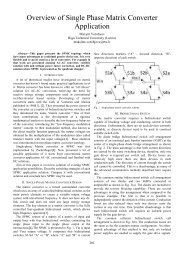
Output Filter for the High-Voltage DC/DC Converter
Output Filter for the High-Voltage DC/DC Converter
Output Filter for the High-Voltage DC/DC Converter

You also want an ePaper? Increase the reach of your titles
YUMPU automatically turns print PDFs into web optimized ePapers that Google loves.
160A<br />
155A<br />
I L<br />
160<br />
140<br />
IL, A<br />
Inductor Current<br />
150A<br />
120<br />
145A<br />
100<br />
140A<br />
80<br />
135A<br />
60<br />
130A<br />
125A<br />
I out<br />
40<br />
<strong>Output</strong> Current, Iout<br />
1 501 18 1001 36 1501 54 2001<br />
72 t, ms<br />
<strong>Output</strong> Current<br />
160<br />
IOUT, A<br />
120A<br />
12.0ms 12.4ms 12.8ms 13.2ms 13.6ms 14.0ms 14.4ms 14.8ms 15.2ms 15.6ms 16.0ms<br />
I(L2) -I(RLoad)<br />
Time<br />
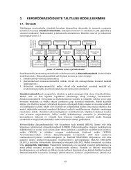
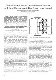
Fig. 7. Inductor current (I L ) and output current (I out )<br />
wave<strong>for</strong>ms with <strong>the</strong> minimum switch duty cycle<br />
Fig. 8 demonstrates rectifier output voltage (U 3 ) and<br />
converter output voltage (U out ) wave<strong>for</strong>ms. The<br />
peak-to-peak output voltage ripple is about 1.5%.<br />
800V<br />
700V<br />
U 3<br />
140<br />
120<br />
100<br />
80<br />
60<br />
40<br />
<strong>Output</strong> <strong>Voltage</strong>, Uout<br />
1 501 18 1001 36 1501 54 72<br />
2001 t, ms<br />
<strong>Output</strong> <strong>Voltage</strong><br />
410<br />
UOUT, V<br />
390<br />
370<br />
600V<br />
350<br />
500V<br />
400V<br />
U out<br />
330<br />
310<br />
300V<br />
290<br />
200V<br />
270<br />
1 501 18 1001 36 1501 54 72 t, ms<br />
2001<br />
100V<br />
0V<br />
Fig. 9. Simulated wave<strong>for</strong>ms of <strong>the</strong> isolated halfbridge<br />
<strong>DC</strong>/<strong>DC</strong> converter with proposed LC-filter<br />
-100V<br />
0s 2ms 4ms 6ms 8ms 10ms 12ms 14ms 16ms<br />
V(RLoad:2) V(L2:1)<br />
Time<br />
Fig. 8. Rectifier output voltage (U 3 ) and converter<br />
output voltage (U out ) with <strong>the</strong> minimum switch duty<br />
cycle<br />
3 <strong>Converter</strong> dynamic response<br />
Above-presented simulations are demonstrating that<br />
filter components were selected properly.<br />
Corresponding voltage and current ripple values are<br />
minimal. Thus, <strong>for</strong> <strong>the</strong> prototype it was decided to<br />
implement <strong>the</strong> laminated iron-core inductor with<br />
inductance value of 5 mH. Two electrolytic<br />
capacitors (EPCOS B437 560 µF, 450 V) will be<br />
connected in series with <strong>the</strong> total capacitance value<br />
of 280 µF.<br />
To test <strong>the</strong> converter dynamic response with <strong>the</strong><br />
selected output filter components <strong>the</strong> generalized<br />
ma<strong>the</strong>matical model of <strong>the</strong> converter was developed<br />
by help of Simplorer® simulation software.<br />
The converter model was tested with <strong>the</strong> maximal<br />
input voltage conditions (4000 V) and during <strong>the</strong><br />
random load step change (see Fig. 9), when <strong>the</strong><br />
output current of <strong>the</strong> converter is changing instantly<br />
from some intermediate value (70 A) to a maximal<br />
value (143 A).<br />
The maximum inductor current ripple is about 10%,<br />
while <strong>the</strong> output current ripple is less than 2%. The<br />
voltage ripple of unregulated output is about 1.5%.<br />
The voltage overshoot during load step change is<br />
14%, which can be fully compensated by <strong>the</strong><br />
appropriated control system algorithm.<br />
Conclusion<br />
<strong>Output</strong> filters play a very important role in <strong>DC</strong>/<strong>DC</strong><br />
converters. Important aspects of converters such as<br />
dynamic response, size and cost are closely related<br />
to <strong>the</strong> components of <strong>the</strong> filter. Small values <strong>for</strong> <strong>the</strong><br />
filter components improve <strong>the</strong> per<strong>for</strong>mance of <strong>the</strong><br />
converters and increase <strong>the</strong> power density, whereas<br />
minimum values should be provided to guarantee <strong>the</strong><br />
filtering objective.<br />
References<br />
[1] D. Vinnikov, „Research, Design and<br />
Implementation of Auxiliary Power Supplies<br />
<strong>for</strong> <strong>the</strong> Light Rail Vehicles”, PhD Thesis,<br />
Tallinn, 2005.<br />
[2] Pressman, A.I., “Switching Power Supply<br />
Design”, Second Edition, McGraw-Hill, 1998.<br />
[3] Billings, K.H., “Switchmode Power Supply<br />
Handbook”, McGraw-Hill, 1989.<br />
121