Output Filter for the High-Voltage DC/DC Converter
Output Filter for the High-Voltage DC/DC Converter
Output Filter for the High-Voltage DC/DC Converter

Create successful ePaper yourself
Turn your PDF publications into a flip-book with our unique Google optimized e-Paper software.
Doctoral school of energy- and geo-technology<br />
January 15–20, 2007. Kuressaare, Estonia<br />
<strong>Output</strong> <strong>Filter</strong> <strong>for</strong> <strong>the</strong> <strong>High</strong>-<strong>Voltage</strong> <strong>DC</strong>/<strong>DC</strong> <strong>Converter</strong><br />
Margus Müür, Dmitri Vinnikov<br />
Tallinn University of Technology<br />
margus.muur@ttu.ee<br />
Abstract<br />
This paper presents <strong>the</strong> output filter analysis and<br />
design <strong>for</strong> <strong>the</strong> high-voltage isolated <strong>DC</strong>/<strong>DC</strong><br />
converter. The topology of <strong>the</strong> filter is <strong>the</strong> second<br />
order low-pass LC but in row with <strong>the</strong> relative<br />
simplicity it demonstrates excellent per<strong>for</strong>mance.<br />
<strong>Filter</strong> steady state analysis as well as simulation<br />
results are discussed.<br />
Keywords<br />
Second order LC-filter, simulation, voltage ripple<br />
Introduction<br />
All <strong>DC</strong>/<strong>DC</strong> converter topologies have an output<br />
filter to supply <strong>the</strong> load with an almost constant<br />
voltage wave<strong>for</strong>m. The output filter has a strong<br />
influence on <strong>the</strong> per<strong>for</strong>mance of <strong>the</strong> converter and an<br />
important impact in its size. One of <strong>the</strong> most<br />
common output filter configuration is <strong>the</strong> LC<br />
network. The values of <strong>the</strong> inductor and capacitor<br />
are determined by <strong>the</strong> output voltage requirements<br />
and by <strong>the</strong> topology of <strong>the</strong> converter.<br />
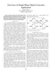
Nowadays <strong>the</strong> Department of Electrical Drives and<br />
Power Electronics of Tallinn University of<br />
Technology is developing a prototype of a brandnew<br />
isolated 3 kV <strong>DC</strong>/<strong>DC</strong> converter <strong>for</strong> <strong>the</strong><br />
supplying internal 350 V <strong>DC</strong>-bus of a commuter<br />
train. The implementation of new 6.5 kV IGBTs<br />
enable fur<strong>the</strong>r simplification of power circuits<br />
(Fig. 1) with no changes in <strong>the</strong> blocking voltage<br />
capability of <strong>the</strong> inverter leg. The <strong>DC</strong>/<strong>DC</strong> converter<br />
parameters are submitted in Table 1.<br />
+U in<br />
L 0 I out<br />
+U out<br />
T 1 D 1 C 1 D 3 D 4<br />
I L<br />
U 3 C 0<br />
TX<br />
T 2 C 2 D 5 D 6<br />
D 2<br />
Fig. 1. <strong>High</strong>-voltage <strong>DC</strong>/<strong>DC</strong> converter circuit<br />
The converter output is connected to an intermediate<br />
<strong>DC</strong>-bus of a train. The function of <strong>the</strong> intermediate<br />
<strong>DC</strong>-bus is to interconnect secondary converters<br />
(output modules). Despite <strong>the</strong> very wide primary<br />
voltage fluctuations <strong>the</strong> output voltage must remain<br />
stable. The desired output voltage regulation<br />
overshoot is only 2.5 % (i.e. 8.75 V), which makes<br />
<strong>the</strong> design of control system and output filter very<br />
challenging.<br />
Table 1. <strong>High</strong>-voltage <strong>DC</strong>/<strong>DC</strong> converter parameters<br />
Parameters<br />
Values<br />
Input voltage range (V) 2200...4000<br />
<strong>Output</strong> voltage (V) 350 ± 2.5%<br />
Peak output current (A), 143<br />
(during 1 min)<br />
Switching frequency (Hz) 1000<br />
In <strong>the</strong> discussed half-bridge topology <strong>the</strong> maximum<br />
duty cycle D (D=t on /T) of each switch is 80% from<br />
<strong>the</strong> half-period at rated load. In practice it means that<br />
isolation trans<strong>for</strong>mer must be specified to provide<br />
maximal current just with <strong>the</strong> minimal input voltage<br />
(i.e., 2200 V). The respective voltage be<strong>for</strong>e <strong>the</strong><br />
output filter (U 3 ) and <strong>the</strong> output filter inductor<br />
current (I L ) are shown in Fig. 2.<br />
Apparently, <strong>the</strong> most demanding operation<br />
conditions to <strong>the</strong> output filter are at <strong>the</strong> maximum<br />
input voltage (i.e., 4000 V) and rated load, when <strong>the</strong><br />
duty cycle D becomes 44% of <strong>the</strong> half-period<br />
(Fig. 3). [1]<br />
I, U<br />
U 3<br />
T<br />
Fig. 2. Diode rectifier output voltage U 3 and<br />
inductor current I L during <strong>the</strong> minimum input<br />
voltage conditions (maximal switch duty cycle)<br />
I, U<br />
I nout<br />
U 3<br />
T<br />
Fig. 3. Diode rectifier output voltage U 3 and<br />
inductor current I L during <strong>the</strong> maximum input<br />
voltage conditions (minimal switch duty cycle)<br />
I L<br />
dI<br />
t<br />
t<br />
I L<br />
118
1 <strong>Output</strong> filter design relations<br />
The output LC-filter is used primarily in power<br />
supplies where voltage regulation is important and<br />
where <strong>the</strong> output current is relatively high and<br />
subject to varying load conditions. This filter is<br />
mainly used in <strong>the</strong> high power applications.<br />
Low-pass LC-filter consists of an input inductor (L 0 )<br />
and an output filter capacitor (C 0 ) (<strong>for</strong> <strong>the</strong> details see<br />
Fig. 1). Inductor L 0 is placed at <strong>the</strong> input of <strong>the</strong> filter<br />
and is in series with <strong>the</strong> output of <strong>the</strong> rectifier circuit.<br />
Since <strong>the</strong> action of an inductor is to oppose any<br />
change in current flow, <strong>the</strong> inductor tends to keep a<br />
constant current flowing to <strong>the</strong> load throughout <strong>the</strong><br />
complete cycle of <strong>the</strong> applied voltage. As a result,<br />
<strong>the</strong> output voltage never reaches <strong>the</strong> peak value of<br />
<strong>the</strong> outgoing trans<strong>for</strong>mer voltage. The reactance of<br />
<strong>the</strong> inductor (X Lo ) reduces <strong>the</strong> amplitude of ripple<br />
voltage without reducing <strong>the</strong> <strong>DC</strong> output voltage by<br />
an appreciable amount (<strong>the</strong> <strong>DC</strong> resistance of <strong>the</strong><br />
inductor is just a few ohms). [2]<br />
The shunt capacitor (C 0 ) charges and discharges at<br />
<strong>the</strong> ripple frequency rate, but <strong>the</strong> amplitude of <strong>the</strong><br />
ripple voltage is relatively small because <strong>the</strong><br />
inductor (L 0 ) tends to keep a constant current<br />
flowing from <strong>the</strong> rectifier circuit to <strong>the</strong> load. In<br />
addition, <strong>the</strong> reactance of <strong>the</strong> shunt capacitor (X Co )<br />
presents low impedance to <strong>the</strong> ripple component<br />
existing at <strong>the</strong> output of <strong>the</strong> filter, and thus shunts<br />
<strong>the</strong> ripple component around <strong>the</strong> load. The capacitor<br />
attempts to hold <strong>the</strong> output voltage relatively<br />
constant at <strong>the</strong> average value of <strong>the</strong> voltage.<br />
The value of <strong>the</strong> filter capacitor (C 0 ) must be<br />
relatively large to present a low opposition (X Co ) to<br />
<strong>the</strong> pulsating current and to store a substantial<br />
charge. The rate of <strong>the</strong> charge <strong>for</strong> <strong>the</strong> capacitor is<br />
limited by <strong>the</strong> low impedance of <strong>the</strong> AC source (<strong>the</strong><br />
trans<strong>for</strong>mer), by <strong>the</strong> small resistance of <strong>the</strong> diode,<br />
and by <strong>the</strong> counter electromotive <strong>for</strong>ce (CEMF)<br />
developed by <strong>the</strong> coil. There<strong>for</strong>e, <strong>the</strong> RC-charge<br />
time constant is short compared to its discharge<br />
time. Consequently, when <strong>the</strong> pulsating voltage is<br />
first applied to <strong>the</strong> LC-filter, <strong>the</strong> inductor (L 0 )<br />
produces a CEMF which opposes <strong>the</strong> constantly<br />
increasing input voltage. The net result is to<br />
effectively prevent <strong>the</strong> rapid charging of <strong>the</strong> filter<br />
capacitor (C 0 ). Thus, instead of reaching <strong>the</strong> peak<br />
value of <strong>the</strong> input voltage, C 0 only charges to <strong>the</strong><br />
average value of <strong>the</strong> input voltage. After <strong>the</strong> input<br />
voltage reaches its peak and decreases sufficiently,<br />
<strong>the</strong> capacitor (C 0 ) attempts to discharge through <strong>the</strong><br />
load resistance (R Load ), what is connected to filter<br />
output. C 0 will only partially discharge because of its<br />
relatively long discharge time constant. The larger is<br />
<strong>the</strong> value of <strong>the</strong> filter capacitor, <strong>the</strong> better <strong>the</strong><br />
filtering action. However, because of physical size,<br />
<strong>the</strong>re is a practical limitation to <strong>the</strong> maximum value<br />
of <strong>the</strong> capacitor.<br />
The first step is to choose an output filter inductor.<br />
In <strong>the</strong> filter inductance calculation is assumed that<br />
<strong>the</strong> inductor current is not discontinuous. It is<br />
discontinuous only when <strong>the</strong> front end of <strong>the</strong><br />
inductor current ramp has dropped to zero and that<br />
this occurs when <strong>the</strong> output <strong>DC</strong> current (minimum)<br />
has fallen to half of <strong>the</strong> filter inductor ripple current<br />
amplitude dI. Then: [2]<br />
ton<br />
ton<br />
dI = 2⋅<br />
Ioutm<br />
= U<br />
L<br />
⋅ = ( U3<br />
−U<br />
out<br />
) ⋅ , (1)<br />
L<br />
L<br />
0<br />
where I outm – minimal output current (half <strong>the</strong> ramp<br />
amplitude dI), U L – voltage drop on filter inductor,<br />
U 3 –rectifier output voltage, U out – converter output<br />
voltage (filtered), t on –switch on-state time, L 0 –filter<br />
inductance to be calculated.<br />
<strong>Output</strong> voltage defining equation [2]<br />
U<br />
out<br />
= U<br />
2⋅t<br />
⋅<br />
T<br />
on<br />
3<br />
, (2)<br />
thus, <strong>the</strong> t on calculation equation is [2]<br />
t<br />
on<br />
Uout<br />
⋅T<br />
2 ⋅U 3<br />
= . (3)<br />
As it was stated be<strong>for</strong>e, <strong>for</strong> <strong>the</strong> values of <strong>the</strong> output<br />
filter components L 0 and C 0 , <strong>the</strong> worst operating<br />
point is at <strong>the</strong> maximum input voltage level and at<br />
<strong>the</strong> rated load conditions (i.e., minimum duty cycle<br />
operation). At this point, <strong>the</strong> operating duty cycle of<br />
<strong>the</strong> inverter switches becomes 44% from <strong>the</strong> halfperiod.<br />
Thus, t on is<br />
t<br />
on<br />
U<br />
out<br />
2⋅U3<br />
⋅T<br />
0.44⋅T<br />
=<br />
2<br />
= . (4)<br />
The voltage U 3 can be derived from Eq. 4<br />
U<br />
U ⋅T<br />
= = 2. 27 ⋅U<br />
0.44⋅T<br />
out<br />
3 out<br />
. (5)<br />
If Eqs. 4 and 5 are placed in Eq. 1, <strong>the</strong>n<br />
0.44 ⋅T<br />
/ 2<br />
dI = 2<br />
L<br />
( 2.27 ⋅U<br />
) ( ) out<br />
−U<br />
out<br />
⋅<br />
= ⋅ Ioutm<br />
The filter inductance equation derived from Eq. 6 is<br />
L<br />
U<br />
= 0. 14 ⋅<br />
⋅T<br />
0<br />
0<br />
(6)<br />
out<br />
. (7)<br />
0<br />
Ioutm<br />
Then if <strong>the</strong> minimum current I outm is specified as 5%<br />
(7.15 A) of <strong>the</strong> nominal output current I nout <strong>the</strong><br />
inductance equation is<br />
L<br />
= 2. 8⋅<br />
U<br />
⋅T<br />
out<br />
. (8)<br />
0<br />
Inout<br />
Based on equation 8, <strong>the</strong> chosen filter inductor<br />
inductance has to be at least 6.86 mH.<br />
The next step is to choose output filter capacitor. It<br />
is assumed that <strong>the</strong> output capacitor size will be<br />
determined by <strong>the</strong> ripple current and ripple voltage<br />
119
specifications only. Assume that <strong>the</strong> ripple voltage at<br />
<strong>the</strong> terminals of C 0 can be 17.5 V (5% of <strong>the</strong> output<br />
voltage). The current change in L 0 during <strong>the</strong> “on”<br />
period will mainly flow into C 0 , and hence <strong>the</strong><br />
capacitance value required to give a voltage change<br />
of 17.5 V can be calculated as follows (<strong>the</strong> following<br />
equation assumes a perfect capacitor with zero ESR)<br />
[3]<br />
C<br />
dI ⋅t<br />
=<br />
U<br />
r<br />
on<br />
0<br />
. (9)<br />
Thus, <strong>the</strong> output filter capacitor capacitance<br />
minimum value is 180 µF, if <strong>the</strong> peak-to-peak ripple<br />
voltage is 5% of <strong>the</strong> output voltage and <strong>the</strong> allowed<br />
filter inductor current ramp amplitude is 10% of <strong>the</strong><br />
nominal output current.<br />
With <strong>the</strong> minor modifications <strong>the</strong> same equations<br />
(1-9) can be applied to <strong>the</strong> maximum duty cycle<br />
operation (minimal amplitude value of U 3 ). Table 2<br />
shows <strong>the</strong> duty cycle variation when input voltage<br />
changes. Fur<strong>the</strong>rmore, it is shown <strong>the</strong> values of L 0<br />
and C 0 to obtain required inductor current ripple<br />
(10%) and output voltage ripple (5%).<br />
Table 2. Calculated filter parameters <strong>for</strong> <strong>the</strong><br />
different operation points<br />
Amplitude value of U 3 440 V 795 V<br />
Switch duty cycle D 0.8(T/2) 0.44(T/2)<br />
Value of L 0 2.45 mH 6.86 mH<br />
Value of C 0 327 µF 180 µF<br />
2.1 Simulation with <strong>the</strong> minimal input voltage<br />
The output voltage pulse amplitude of an isolation<br />
trans<strong>for</strong>mer is minimal and <strong>the</strong> pulse width is<br />
longest (on-state time of each IGBT transistor is<br />
0.4 T).<br />
Fig. 5 demonstrates simulated inductor current (I L )<br />
and output current (I out ) wave<strong>for</strong>ms. The peak-topeak<br />
inductor current ripple is not exceeding 5%,<br />
which is in <strong>the</strong> good agreement with <strong>the</strong><br />
requirements. <strong>Output</strong> current ripple is less than 1%.<br />
150A<br />
145A<br />
140A<br />
135A<br />
130A<br />
12.0ms 12.4ms 12.8ms 13.2ms 13.6ms 14.0ms 14.4ms 14.8ms 15.2ms 15.6ms 16.0ms<br />
I L<br />
I out<br />
Fig. 5. Inductor current (I L ) and output current (I out )<br />
wave<strong>for</strong>ms with <strong>the</strong> maximum switch duty cycle<br />
Fig. 6 demonstrates rectifier output voltage (U 3 ) and<br />
converter output voltage (U out ) wave<strong>for</strong>ms. The<br />
peak-to-peak output voltage ripple is less than 1%.<br />
2 <strong>Output</strong> filter simulations<br />
PSpice simulation circuit of <strong>the</strong> output LC-filter <strong>for</strong><br />
a high voltage <strong>DC</strong>/<strong>DC</strong> converter is shown in Fig. 4.<br />
500V<br />
400V<br />
U 3<br />
300V<br />
U out<br />
200V<br />
100V<br />
0V<br />
Fig. 4. PSpice simulation circuit of <strong>the</strong> output<br />
LC-filter<br />
All used components are ideal, what means that <strong>the</strong><br />
voltage drops were not considered in simulations. To<br />
simplify <strong>the</strong> circuit only <strong>the</strong> resistive load was used.<br />
Two pulse voltage sources were used to simulate <strong>the</strong><br />
trans<strong>for</strong>mer output voltage. For finding trans<strong>for</strong>mer<br />
output voltage amplitude Eq. 2 was used.<br />
The output filter was proven in two different<br />
conditions: with maximum switch duty cycle<br />
(minimal converter input voltage U in ) and with<br />
minimum switch duty cycle (maximal converter<br />
input voltage U in ). Both simulations were made with<br />
maximum load that is most demanding <strong>for</strong> <strong>the</strong><br />
output filter design. Values of filter elements to be<br />
tested are L 0 =7 mH and C 0 =180 µF.<br />
-100V<br />
0s 2ms 4ms 6ms 8ms 10ms 12ms 14ms 16ms<br />
V(D3:2) V(RLoad:2)<br />
Time<br />
Fig. 6. Rectifier output voltage (U 3 ) and converter<br />
output voltage (U out ) with <strong>the</strong> maximum switch duty<br />
cycle<br />
2.2 Simulation with <strong>the</strong> maximal input voltage<br />
The output voltage pulse amplitude of an isolation<br />
trans<strong>for</strong>mer is reaching its maximum and <strong>the</strong> pulse<br />
width is shortest (on-state time of each IGBT<br />
transistor is 0.22 T).<br />
Fig. 7 demonstrates simulated inductor current (I L )<br />
and output current (I out ) wave<strong>for</strong>ms. The peak-topeak<br />
inductor current ripple is not exceeding 10%,<br />
which is in <strong>the</strong> good agreement with <strong>the</strong><br />
requirements. <strong>Output</strong> current ripple is about 1.5%.<br />
120
160A<br />
155A<br />
I L<br />
160<br />
140<br />
IL, A<br />
Inductor Current<br />
150A<br />
120<br />
145A<br />
100<br />
140A<br />
80<br />
135A<br />
60<br />
130A<br />
125A<br />
I out<br />
40<br />
<strong>Output</strong> Current, Iout<br />
1 501 18 1001 36 1501 54 2001<br />
72 t, ms<br />
<strong>Output</strong> Current<br />
160<br />
IOUT, A<br />
120A<br />
12.0ms 12.4ms 12.8ms 13.2ms 13.6ms 14.0ms 14.4ms 14.8ms 15.2ms 15.6ms 16.0ms<br />
I(L2) -I(RLoad)<br />
Time<br />
Fig. 7. Inductor current (I L ) and output current (I out )<br />
wave<strong>for</strong>ms with <strong>the</strong> minimum switch duty cycle<br />
Fig. 8 demonstrates rectifier output voltage (U 3 ) and<br />
converter output voltage (U out ) wave<strong>for</strong>ms. The<br />
peak-to-peak output voltage ripple is about 1.5%.<br />
800V<br />
700V<br />
U 3<br />
140<br />
120<br />
100<br />
80<br />
60<br />
40<br />
<strong>Output</strong> <strong>Voltage</strong>, Uout<br />
1 501 18 1001 36 1501 54 72<br />
2001 t, ms<br />
<strong>Output</strong> <strong>Voltage</strong><br />
410<br />
UOUT, V<br />
390<br />
370<br />
600V<br />
350<br />
500V<br />
400V<br />
U out<br />
330<br />
310<br />
300V<br />
290<br />
200V<br />
270<br />
1 501 18 1001 36 1501 54 72 t, ms<br />
2001<br />
100V<br />
0V<br />
Fig. 9. Simulated wave<strong>for</strong>ms of <strong>the</strong> isolated halfbridge<br />
<strong>DC</strong>/<strong>DC</strong> converter with proposed LC-filter<br />
-100V<br />
0s 2ms 4ms 6ms 8ms 10ms 12ms 14ms 16ms<br />
V(RLoad:2) V(L2:1)<br />
Time<br />
Fig. 8. Rectifier output voltage (U 3 ) and converter<br />
output voltage (U out ) with <strong>the</strong> minimum switch duty<br />
cycle<br />
3 <strong>Converter</strong> dynamic response<br />
Above-presented simulations are demonstrating that<br />
filter components were selected properly.<br />
Corresponding voltage and current ripple values are<br />
minimal. Thus, <strong>for</strong> <strong>the</strong> prototype it was decided to<br />
implement <strong>the</strong> laminated iron-core inductor with<br />
inductance value of 5 mH. Two electrolytic<br />
capacitors (EPCOS B437 560 µF, 450 V) will be<br />
connected in series with <strong>the</strong> total capacitance value<br />
of 280 µF.<br />
To test <strong>the</strong> converter dynamic response with <strong>the</strong><br />
selected output filter components <strong>the</strong> generalized<br />
ma<strong>the</strong>matical model of <strong>the</strong> converter was developed<br />
by help of Simplorer® simulation software.<br />
The converter model was tested with <strong>the</strong> maximal<br />
input voltage conditions (4000 V) and during <strong>the</strong><br />
random load step change (see Fig. 9), when <strong>the</strong><br />
output current of <strong>the</strong> converter is changing instantly<br />
from some intermediate value (70 A) to a maximal<br />
value (143 A).<br />
The maximum inductor current ripple is about 10%,<br />
while <strong>the</strong> output current ripple is less than 2%. The<br />
voltage ripple of unregulated output is about 1.5%.<br />
The voltage overshoot during load step change is<br />
14%, which can be fully compensated by <strong>the</strong><br />
appropriated control system algorithm.<br />
Conclusion<br />
<strong>Output</strong> filters play a very important role in <strong>DC</strong>/<strong>DC</strong><br />
converters. Important aspects of converters such as<br />
dynamic response, size and cost are closely related<br />
to <strong>the</strong> components of <strong>the</strong> filter. Small values <strong>for</strong> <strong>the</strong><br />
filter components improve <strong>the</strong> per<strong>for</strong>mance of <strong>the</strong><br />
converters and increase <strong>the</strong> power density, whereas<br />
minimum values should be provided to guarantee <strong>the</strong><br />
filtering objective.<br />
References<br />
[1] D. Vinnikov, „Research, Design and<br />
Implementation of Auxiliary Power Supplies<br />
<strong>for</strong> <strong>the</strong> Light Rail Vehicles”, PhD Thesis,<br />
Tallinn, 2005.<br />
[2] Pressman, A.I., “Switching Power Supply<br />
Design”, Second Edition, McGraw-Hill, 1998.<br />
[3] Billings, K.H., “Switchmode Power Supply<br />
Handbook”, McGraw-Hill, 1989.<br />
121