thin film materials based on v-vi semiconductors and ... - ECT2008
thin film materials based on v-vi semiconductors and ... - ECT2008
thin film materials based on v-vi semiconductors and ... - ECT2008

Create successful ePaper yourself
Turn your PDF publications into a flip-book with our unique Google optimized e-Paper software.
THIN FILM MATERIALS BASED ON V-VI SEMICONDUCTORS AND<br />
BINARY SKUTTERUDITE FOR APPLICATIONS ON THERMOELECTRIC<br />
MICROSENSORS<br />
A. Boulouz 1 , L. Koutti 1 , A. Giani 2 , M. Boulouz 1 , J. Shumann 3 ,<br />
<strong>and</strong> F. Pascal-Delannoy 2<br />
1-Faculté des Sciences, Université Ibn Zohr, 80000 Agadir, Morocco<br />
2-Institut d’Electr<strong>on</strong>ique de Sud, IES, Université M<strong>on</strong>tpellier II (cc 075),<br />
Place E. Bataill<strong>on</strong>, 34095 M<strong>on</strong>tpellier, cedex 05, France<br />
3-Institute of Solid State <strong>and</strong> Materials Research, IFW Helmholtzstrasse 20,<br />
D-01069 Dresden, Germany<br />
C<strong>on</strong>tact author: abdellah.boulouz@graduates.centraliens.net<br />
Abstract<br />
The characteristics of Bi 2 Te 3 ,<br />
Sb 2 Te 3 <strong>and</strong> (Bi 1-x Sb x ) 2 Te 3 alloy <str<strong>on</strong>g>film</str<strong>on</strong>g>s<br />
growth by MOCVD will be presented. The<br />
values of Seebeck coefficient (α(T)) at<br />
room temperature for Bi 2 Te 3 , Sb 2 Te 3 , <strong>and</strong><br />
(Bi 1-x Sb x ) 2 Te 3 with x=0.77 are found to be<br />
–220 µV/K, +110 µV/K <strong>and</strong> +240 µV/K,<br />
respectively. In an other h<strong>and</strong>, the<br />
thermoelectric CoSb 3 <str<strong>on</strong>g>film</str<strong>on</strong>g>s are deposited<br />
<strong>on</strong> oxidised Si(100) <strong>and</strong> ceramic Al 2 O 3<br />
substrates using magnetr<strong>on</strong> dc sputtering<br />
technique.<br />
To evaluate the efficiency of some<br />
elaborated <str<strong>on</strong>g>film</str<strong>on</strong>g>s, we present results of gas<br />
<strong>and</strong> pressure micro-sensor<br />
Introducti<strong>on</strong><br />
The efficiency of thermoelectric <str<strong>on</strong>g>materials</str<strong>on</strong>g><br />
is usually characterised by the<br />
dimensi<strong>on</strong>less of the product ZT where Z<br />
is known as thermoelectric Figure of merit<br />
<strong>and</strong> T is absolute temperature (in Kel<strong>vi</strong>n).<br />
There are two differents approaches which<br />
can be used for preparing high ZT<br />
<str<strong>on</strong>g>materials</str<strong>on</strong>g>: (1) the multi quantum well<br />
structures (MQW) with quantum<br />
c<strong>on</strong>finement effects <strong>and</strong> (2) the c<strong>on</strong>cept of<br />
reducing lattice thermal c<strong>on</strong>ducti<strong>vi</strong>ty K<br />
(especially in high temperature<br />
applicati<strong>on</strong>s) in PGEC (Ph<strong>on</strong><strong>on</strong> Glass<br />
Electr<strong>on</strong> Crystal) systems. The c<strong>on</strong>cept of<br />
MQW is mainly dealt with <str<strong>on</strong>g>thin</str<strong>on</strong>g> <str<strong>on</strong>g>film</str<strong>on</strong>g>s <strong>and</strong><br />
superlattices [3-5]. CoSb 3 ) are studied<br />
mainly as bulk <str<strong>on</strong>g>materials</str<strong>on</strong>g> [6].<br />
The Figure of merit Z or the potential of a<br />
material for thermoelectric applicati<strong>on</strong>s is<br />
determined by [2]:<br />
Z= α 2 /ρk (1)<br />
k = k L + k e (2)<br />
Where α represent the Seebeck coefficient,<br />
ρ the electrical resisti<strong>vi</strong>ty, <strong>and</strong> k the total<br />
thermal c<strong>on</strong>ducti<strong>vi</strong>ty (the lattice (ph<strong>on</strong><strong>on</strong><br />
part) k L <strong>and</strong> electr<strong>on</strong>ic k e c<strong>on</strong>tributi<strong>on</strong>s) [1-<br />
2]. The power factor, α 2 /ρ, is typically<br />
optimized as a functi<strong>on</strong> of carrier<br />
c<strong>on</strong>centrati<strong>on</strong>, through doping, to give the<br />
largest ZT.<br />
From equati<strong>on</strong> 1, the value of Z can be<br />
raised by decreasing k L. It can also be<br />
raised by increasing α 2 /ρ. However, 1/ρ<br />
(electrical c<strong>on</strong>dicti<strong>vi</strong>ty) is related<br />
proporti<strong>on</strong>aly to the Ke through the<br />
Wiedmann-Franz Law, <strong>and</strong> the ratio is<br />
essentially c<strong>on</strong>stant at a given temperature.<br />
Experimental details<br />
The MOCVD with an horiz<strong>on</strong>tal quartz<br />
reactor was used to elaborat a binary<br />
Bi 2 Te 3 <strong>and</strong> Sb 2 Te 3 , <strong>and</strong> ternary (Bi 1-x<br />
Sb x ) 2 Te 3 alloys <strong>on</strong> pyrex substrate with<br />
total H 2 gas flow rate of 6 litre/minute. All<br />
the <str<strong>on</strong>g>film</str<strong>on</strong>g>s were prepared at a pressure of<br />
700 Torr. The high purity (a few parts per<br />
billi<strong>on</strong>) precursors for Bi, Sb <strong>and</strong> Te were<br />
Trimethylbismuth, Triethylantim<strong>on</strong>y <strong>and</strong><br />
Diethyltellurium, respectively [7-8]. The<br />
depositi<strong>on</strong> rate for all the <str<strong>on</strong>g>film</str<strong>on</strong>g>s was of the<br />
O-16-1
order 0.34 µm/h <strong>and</strong> the final thickness<br />
deposited in all cases was around 600 nm.<br />
DC-magnetr<strong>on</strong> sputtering technique with<br />
an ultra high vacuum chamber with a base<br />
pressure less than 10 -9 mbar was used to<br />
growth binary skutterudite CoSb 3 . The<br />
<str<strong>on</strong>g>film</str<strong>on</strong>g>s were deposited <strong>on</strong> oxidised Si(100)<br />
<strong>and</strong> ceramic Al 2 O 3 substrates under arg<strong>on</strong><br />
atmosphere. During depositi<strong>on</strong>, the<br />
chamber pressure was at 7x10 -3 mbar while<br />
the substrate temperature was kept at<br />
200°C <strong>and</strong> 20°C. The applied dc-power in<br />
the sputtering target was 150W. The rate of<br />
depositi<strong>on</strong> was kept at around 6.3nm/min<br />
<strong>and</strong> the final thickness for CoSb 3 <str<strong>on</strong>g>film</str<strong>on</strong>g>s was<br />
about 190nm.<br />
Results <strong>and</strong> discussi<strong>on</strong><br />
Figure 1 shows the X-ray diffractogram of<br />
a typical (Bi 1-x Sb x ) 2 Te 3 <str<strong>on</strong>g>thin</str<strong>on</strong>g> <str<strong>on</strong>g>film</str<strong>on</strong>g> with x =<br />
0.77. The presence of (006), (015) <strong>and</strong><br />
(110) plans c<strong>on</strong>firms the polycristalline<br />
structure of the <str<strong>on</strong>g>thin</str<strong>on</strong>g> layers.<br />
The compositi<strong>on</strong> of the deposited Bi 2 Te 3<br />
<strong>and</strong> Sb 2 Te 3 <str<strong>on</strong>g>film</str<strong>on</strong>g>s is measured by means of<br />
the energy dispersive X-ray (EDX)<br />
microanalyser.<br />
Intensity (a.u.)<br />
(006)<br />
(015)<br />
(110)<br />
(Bi 1-x<br />
Sb x<br />
) 2<br />
Te 3<br />
x = 0.77 / BST2<br />
(205)<br />
Intensity (a.u.)<br />
3500<br />
3000<br />
2500<br />
2000<br />
1500<br />
1000<br />
500<br />
(310)<br />
(310)<br />
0<br />
0 20 40 60 80 100 120 140 160<br />
Diffracti<strong>on</strong> angle<br />
CoSb 3<br />
annealed <str<strong>on</strong>g>film</str<strong>on</strong>g><br />
as deposited <str<strong>on</strong>g>film</str<strong>on</strong>g><br />
Fig 2: X-ray diffracti<strong>on</strong> diagram of CoSb 3<br />
Thin <str<strong>on</strong>g>film</str<strong>on</strong>g> elaborated<br />
The lattice parameter of the cubic cell is<br />
found to be around a = 9.0358 Å which is<br />
very close to the value of the bulk<br />
<str<strong>on</strong>g>materials</str<strong>on</strong>g> reported earlier by Fleurial et al.<br />
[30] (a = 9.0385 Å).<br />
From the X-ray diffracti<strong>on</strong>, it can be seen<br />
that the polycrystalline grains in the <str<strong>on</strong>g>film</str<strong>on</strong>g>s<br />
exhibit a str<strong>on</strong>g preferred alignment of the<br />
cubic (310) axis perpendicular to the<br />
substrate surface which indicates the<br />
skutterudite phase of CoSb 3 <strong>on</strong>ly.<br />
Seebeck coefficient (µV/K)<br />
280<br />
260<br />
240<br />
220<br />
200<br />
180<br />
160<br />
140<br />
120<br />
100<br />
80<br />
(Bi 1-x<br />
Sb x<br />
) 2<br />
Te 3<br />
Seebeck coefficient<br />
Electrical resisti<strong>vi</strong>ty<br />
0,5 0,6 0,7 0,8 0,9 1,0<br />
%Sb (x)<br />
140<br />
120<br />
100<br />
80<br />
60<br />
40<br />
20<br />
0<br />
Electrical resisti<strong>vi</strong>ty (µΩ.m)<br />
Tc = 450 °C<br />
Tc = 470 °C<br />
5 10 15 20 25 30 35<br />
Diffracti<strong>on</strong> angle<br />
Fig 1: X-ray diffracti<strong>on</strong> diagram of (Bi 1-x Sb x ) 2 Te 3<br />
Thin <str<strong>on</strong>g>film</str<strong>on</strong>g> elaborated at Tc =450°C <strong>and</strong> TC =<br />
470°C<br />
An annealing at 350°C for 3 hours under<br />
arg<strong>on</strong> atmosphere does not have any<br />
influence <strong>on</strong> the quality of crystallisati<strong>on</strong><br />
of the skutterudite CoSb 3 <str<strong>on</strong>g>film</str<strong>on</strong>g>s (figure 2).<br />
Fig 3: Seebeck coefficient <strong>and</strong> electrical resisti<strong>vi</strong>ty<br />
of (Bi 1-x Sb x ) 2 Te 3 Thin <str<strong>on</strong>g>film</str<strong>on</strong>g> as functi<strong>on</strong> of %Sb (x).<br />
Figure 3 illustrates the variati<strong>on</strong> of the<br />
Seebeck coefficient <strong>and</strong> electrical<br />
resisti<strong>vi</strong>ty of (Bi 1-x Sb x ) 2 Te 3 <str<strong>on</strong>g>thin</str<strong>on</strong>g> <str<strong>on</strong>g>film</str<strong>on</strong>g>s as a<br />
functi<strong>on</strong> of the antim<strong>on</strong>y compositi<strong>on</strong> x in<br />
the layers. It is observed that for x ≤ 0.30,<br />
The room temperature values of Seebeck<br />
coefficient (α), Hall mobility (µ), electrical<br />
resisti<strong>vi</strong>ty (ρ), <strong>and</strong> carrier c<strong>on</strong>centrati<strong>on</strong> for<br />
optimal n-type Bi 2 Te 3 <strong>and</strong> p-type Sb 2 Te 3<br />
O-16-2
<strong>and</strong> BiSbTe p-type ternary (Bi 1-x Sb x ) 2 Te 3<br />
(x=0.77) <str<strong>on</strong>g>film</str<strong>on</strong>g>s, are presented in the table 1.<br />
Seebeck coefficient (µV/K)<br />
0<br />
-100<br />
-200<br />
-300<br />
ES 193n17 <strong>on</strong> Si<br />
annealed at 350°C/Ar/5h<br />
CoSb 3<br />
wafer 1<br />
wafer 2<br />
wafer 3<br />
300 400 500 600 700<br />
Temperature (K)<br />
Fig4: Reproductibility of temperature dependence<br />
of seebeck coefficient of CoSb 3 <str<strong>on</strong>g>thin</str<strong>on</strong>g> <str<strong>on</strong>g>film</str<strong>on</strong>g> deposited<br />
<strong>on</strong> silic<strong>on</strong> substrate.<br />
The variati<strong>on</strong> of the Seebeck coefficient<br />
(α ) is shown in Figure 4 for the annealed<br />
CoSb 3 <str<strong>on</strong>g>film</str<strong>on</strong>g>s <strong>on</strong> two different substrates in<br />
the temperature range between 300 <strong>and</strong><br />
700 K.<br />
The value of α in the as-deposited <str<strong>on</strong>g>film</str<strong>on</strong>g> is<br />
found to be near zero at 300K. After the<br />
first measuring cycle up to 700K <strong>and</strong> also<br />
for the sample annealed at 350°C, the<br />
maximum value of -250 µV/K is attained.<br />
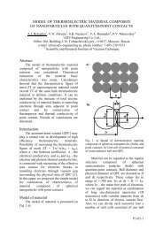
The sensor design that can work as gas<br />
detecti<strong>on</strong> or pressure sensor is presented in<br />
Figure 5. This sensor is made of a resistor<br />
(heating element) <strong>and</strong> an integrated<br />
thermocouple deposited <strong>on</strong> a thermally<br />
isolated membrane. In both cases the active<br />
thermoelement is deposited through two<br />
complementary masks of nickel. Thus n-<br />
Bi 2 Te 3 <strong>and</strong> p-(Bi 1_x Sb x ) 2 Te 3 basic<br />
<str<strong>on</strong>g>materials</str<strong>on</strong>g> are realised by MOCVD under<br />
optimal growth c<strong>on</strong>diti<strong>on</strong>s setting in<br />
pre<strong>vi</strong>ous secti<strong>on</strong>.<br />
We have found the measure of temperature<br />
in the centre of the active z<strong>on</strong>e in the<br />
resistance as a functi<strong>on</strong> of an injected<br />
current by using three different means: an<br />
infrared camera, a discrete thermocouple,<br />
<strong>and</strong> the integrated thermocouple.<br />
For the infrared camera, we have<br />
determined the emissi<strong>on</strong> of the <str<strong>on</strong>g>materials</str<strong>on</strong>g><br />
Bi 2 Te 3 <strong>and</strong> (Bi 1-x Sb x ) 2 Te 3 compared to the<br />
blackbody <strong>on</strong>e which is equal to 1. The<br />
material <strong>on</strong>e has been measured <strong>and</strong> equal<br />
to 0.61. the good functi<strong>on</strong> of this<br />
thermocouple is accuracy verified. The<br />
measure obtained by thermocouple type E<br />
<strong>on</strong> c<strong>on</strong>tact with the resistance field<br />
presents a difference in comparis<strong>on</strong> with<br />
that of infrared camera. This difference<br />
increases with the heating courant: it is due<br />
to the heating dissipati<strong>on</strong> that crosses<br />
through the thermocouple by c<strong>on</strong>ducti<strong>on</strong>. It<br />
unfortunately plays the role of a heat sink.<br />
Generally, the rule of variati<strong>on</strong> of the<br />
resistance temperature is I 2 . This means the<br />
heating by Joule effect of the charge.<br />
X'<br />
Electric c<strong>on</strong>tact<br />
(Ni + Cu)<br />
Electric c<strong>on</strong>tact<br />
(Ni + Cu)<br />
3,5mm<br />
4mm<br />
N<br />
P<br />
Y'<br />
Y<br />
kapt<strong>on</strong> (20 µm)<br />
Resistance<br />
P-N juncti<strong>on</strong><br />
N<br />
kapt<strong>on</strong> ( 20 µm)<br />
5,5mm 5mm<br />
ohmic c<strong>on</strong>tact ( Ni+ Cu)<br />
(Bi 1-x Sb x ) 2 Te 3 (P-type) x = 77,4 %<br />
Bi 2 Te 3 ( N-type)<br />
Fr<strong>on</strong>t side Vue<br />
X<br />
XX' Cross Vue<br />
N P<br />
YY' Cross Vue<br />
Thermocouple<br />
Fig 5: Schematic design of gas <strong>and</strong> pressure microsensor<br />
using n-type Bi 2 Te 3 <strong>and</strong> p-type (Bi 1-x Sb x ) 2 Te 3<br />
for x=0.77 <str<strong>on</strong>g>film</str<strong>on</strong>g>s.<br />
In Figure 6 we represent the tensi<strong>on</strong><br />
variati<strong>on</strong> (V pr - V atm ) of the sensor for<br />
different powers of heating. V pr is the<br />
thermoelectric tensi<strong>on</strong> got by the<br />
thermocouple at a pressure value <strong>and</strong> V atm<br />
Ni<br />
Cu<br />
O-16-3
the tensi<strong>on</strong> measure at atmospheric<br />
pressure.<br />
V p<br />
- V atm<br />
(mV)<br />
40<br />
35<br />
30<br />
25<br />
20<br />
15<br />
10<br />
5<br />
P = 59 mW<br />
P = 38 mW<br />
V(V) measured by integrated thermoucouple<br />
0,05<br />
0,04<br />
0,03<br />
0,02<br />
0,01<br />
0,00<br />
0 2500 5000 7500 10000 12500 15000<br />
Time en (ms)<br />
T f -T 0 = 80°C<br />
T f -T 0 = 120°C<br />
T f -T 0 = 40°C<br />
0<br />
1E-4 1E-3 0,01 0,1 1 10 100 1000<br />
Pressure (torr)<br />
Fig 6: V(mV) (1) variati<strong>on</strong> as functi<strong>on</strong> of the<br />
pressure in the chamber<br />
From 10 -4 to 10 -2 torr, the resistance<br />
changes from the heat caused by thermal<br />
radiance. The resp<strong>on</strong>se of sensor in this<br />
part is c<strong>on</strong>stant. From 10 -3 to 10 torr, the<br />
changes of heat are caused by c<strong>on</strong>vecti<strong>on</strong>,<br />
the coefficient H approaches to the<br />
Knudsen formula <strong>and</strong> it is a functi<strong>on</strong> of the<br />
pressure [10-11]. From 10 to 760 torr, the<br />
resp<strong>on</strong>se of the sensor is saturated because<br />
the exchanges caused by c<strong>on</strong>vecti<strong>on</strong> are<br />
c<strong>on</strong>stants.<br />
Figure 7, shows the V(mv) voltage<br />
variati<strong>on</strong> as functi<strong>on</strong> of time.<br />
V t = V max (1-e -t/τ )<br />
where V t = V at time t, <strong>and</strong> τ=time<br />
c<strong>on</strong>stant of sensor.<br />
when t = τ, (t = <strong>on</strong>e time c<strong>on</strong>stant) :<br />
V τ = V max (1-e -1 ) = V max (0.63)<br />
So, <strong>on</strong>e time c<strong>on</strong>stant or rep<strong>on</strong>se time is the<br />
time it takes for the V(t) to reach 63% of its<br />
maximum value Vmax. τ = 600ms.<br />
C<strong>on</strong>clusi<strong>on</strong><br />
The BiSbTe <str<strong>on</strong>g>thin</str<strong>on</strong>g> <str<strong>on</strong>g>film</str<strong>on</strong>g>s are prepared by<br />
MOCVD technique. From the room<br />
temperature Seebeck coefficient (α)<br />
measurement, the values of α for Bi 2 Te 3 ,<br />
Sb 2 Te 3 , <strong>and</strong> (Bi 1-x Sb x ) 2 Te 3 with x=0.77 are<br />
found to be –220 µV/K, +110µV/K <strong>and</strong> +<br />
240 µV/K respectively.<br />
Fig 7: Variati<strong>on</strong> of thermocouple voltage as<br />
functi<strong>on</strong> of the time (ms)<br />
The CoSb 3 <str<strong>on</strong>g>film</str<strong>on</strong>g>s with relatively high<br />
Seebeck coefficients can be prepared by dc<br />
magnetr<strong>on</strong> sputtering using compound<br />
targets. The preparati<strong>on</strong> process has to be<br />
carefully optimized, For the pressure<br />
sensor, the optimal sensibility is observed<br />
for the pressure range: 10 -4 to 10 torr. The<br />
resp<strong>on</strong>se time of the sensor, about 600 ms,<br />
does not vary with the injected electric<br />
power. Good sensibility is due to high<br />
thermoelectric power of the <str<strong>on</strong>g>thin</str<strong>on</strong>g> <str<strong>on</strong>g>film</str<strong>on</strong>g>s <strong>and</strong><br />
the good reproducibility is obtained.<br />
References<br />
[1] P.Magri, C.Boulanger <strong>and</strong> J.M.Lecuire,<br />
J.Mater.Chem.6 (5) (1996)773.<br />
[2] H.Kaibe, Y.Tanaka, M.Sakata <strong>and</strong> I.Nishida,<br />
J.Phys.Chem.Solids, 50 (1989)945.<br />
[3] Rama Venkatasubramanian, Phys. Rev. B 61, (2000)<br />
3091.<br />
[4] Rama Venkatasubramanian, Thomas Colpitts, Brooks<br />
O’Quinn, S<strong>and</strong>ra Liu, NadiaEl Masry, <strong>and</strong> Michael<br />
Lam<strong>vi</strong>k, Appl. Phys. Lett. 75, (1999) 1104.<br />
[5] R. Venkatasubramanian, T. Colpitts, E.Watko, M.<br />
Lam<strong>vi</strong>k, <strong>and</strong> N. ElMasry, J. OfCryst. Growth 170, (1997)<br />
817.<br />
[6] G. S. Nolas, D. T. Morelli, <strong>and</strong> Terry M. Tritt, Annu.<br />
Rev. Mater. Sci. 29, (1999) 89.<br />
[7] B. Aboulfarah, A. Mzerd, A. Giani, A. Boulouz F.<br />
Pascal-Delannoy, A. Foucaran,<br />
<strong>and</strong> A.Boyer, Materials Chemistry <strong>and</strong> Physics 62,<br />
(2000) 179.<br />
[8] A. Giani, A. Boulouz, F. Pascal-Delannoy, A.<br />
Foucaran, <strong>and</strong> A. Boyer, Mater. Sci. A Eng. B 64, (1999)<br />
19.<br />
[9] J. P. Fleurial, T. Caillat <strong>and</strong> A.Borshevsky, Proc. 16 th<br />
Internati<strong>on</strong>alC<strong>on</strong>ference <strong>on</strong> Thermoelectrics, Dresden<br />
(Germany), IEEE Catalog number 97 th 8291, (1997) 1.<br />
[10] T. Shioyama, T. Takiguchi, S. Ogwa, J. Vac. Sci.<br />
Technol. 15 (2) (1978) 761.<br />
[11] L.M. G<strong>on</strong>calves, J.G. Rocha, C. Couto, P. Alpuim,<br />
Gao Min, D.M. Rowe <strong>and</strong> J.H.Correia, J.<br />
Micromechanics & Microengineering 17 (2007)<br />
O-16-4