IBM 130nm CMOS Process - Electronics Design Group
IBM 130nm CMOS Process - Electronics Design Group
IBM 130nm CMOS Process - Electronics Design Group
You also want an ePaper? Increase the reach of your titles
YUMPU automatically turns print PDFs into web optimized ePapers that Google loves.
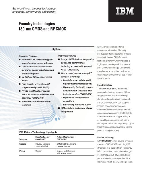
State-of-the-art process technology<br />
for optimal performance and density<br />
Foundry technologies<br />
130-nm <strong>CMOS</strong> and RF <strong>CMOS</strong><br />
Standard Features<br />
Twin-well <strong>CMOS</strong> technology on<br />
nonepitaxial p- doped substrate<br />
Low-resistance cobalt-silicide<br />
n+ and p+ doped polysilicon and<br />
diffusion regions<br />
Up to three thick copper wiring<br />
levels<br />
Four to eight levels of global<br />
copper metal (<strong>CMOS</strong> 8SFG)<br />
Five to eight levels of copper<br />
metal with an Al-Cu-Al last metal<br />
sequence (<strong>CMOS</strong> 8RF)<br />
Wire-bond or C4 solder-bump<br />
terminals<br />
Highlights<br />
<strong>IBM</strong> 130-nm Technology Highlights<br />
Base Technology Related Technology<br />
Category <strong>CMOS</strong> 8SFG <strong>CMOS</strong> 8RF<br />
Optional Features<br />
Range of FET devices to optimize<br />
power and performance,<br />
including an isolated triple-well<br />
NFET (<strong>CMOS</strong> 8RF)<br />
Vast array of passive analog RF<br />
devices, including:<br />
– Low-tolerance resistors with<br />
high and low sheet resistivity<br />
– High-quality factor (Q) copper<br />
and aluminum inductors and<br />
inductor models (<strong>CMOS</strong> 8RF)<br />
– High-value, low-tolerance<br />
capacitors<br />
– Electrically writable e-fuses<br />
<strong>IBM</strong> and third-party logic library<br />
design tools<br />
<strong>Process</strong> Industry-standard <strong>CMOS</strong> 8SFG additional<br />
130-nm <strong>CMOS</strong> passive devices<br />
Wiring Copper Copper and aluminum<br />
with analog metal<br />
<strong>IBM</strong> Microelectronics offers a<br />
comprehensive suite of foundry<br />
products and services for its industrystandard<br />
130-nm <strong>CMOS</strong>-based<br />
technology family, which includes a<br />
high-speed analog radio frequency<br />
(RF) <strong>CMOS</strong> technology. Customers<br />
can choose appropriate devices and<br />
design tools to match their application<br />
requirements.<br />
Base technology<br />
The <strong>IBM</strong> <strong>CMOS</strong> 8SFG advanced<br />
process technology features 130-nm<br />
lithography. The fine lines and high<br />
densities characterizing this state-ofthe-art<br />
silicon process can support<br />
leading-edge microprocessors,<br />
communications and computer dataprocessing<br />
applications. <strong>CMOS</strong> 8SFG<br />
uses low-resistance copper wiring at<br />
all metal levels, enabling high wiring<br />
density with minimal timing delays. Up to<br />
three thick copper wiring metal options<br />
provide design flexibility.<br />
Related technology<br />
<strong>IBM</strong> <strong>CMOS</strong> 8RF offers several enhancements<br />
to <strong>CMOS</strong> 8SFG including FET<br />
structures that support high-frequency<br />
RF-compatible models, a broad range<br />
of optional passive devices and copper<br />
and aluminum wiring with a thick<br />
last metal. A high-quality analog design
kit ensures close correlation between<br />
simulated and measured performance.<br />
In addition, the technology maintains<br />
compatible design rules with the corresponding<br />
levels in <strong>CMOS</strong> 8SFG.<br />
<strong>CMOS</strong> 8RF is an ideal semiconductor<br />
technology for low-cost, high-performance<br />
wireless applications such as<br />
Bluetooth technologies, local area<br />
networks, handsets and global positioning<br />
systems.<br />
For more information<br />
For more information, contact <strong>IBM</strong> at<br />
foundry@us.ibm.com<br />
<strong>CMOS</strong> Specifications (common to 130-nm technology family)<br />
Lithography<br />
Voltage (V DD )<br />
Additional power supply options<br />
130 nm<br />
1.2 V or 1.5 V<br />
2.5 V / 3.3 V I/O<br />
Standard NFET / PFET<br />
L min 0.24 µm<br />
L p 0.22 µm<br />
V t<br />
0.355 V / -0.30 V<br />
I Dsat<br />
530 mA / 210 mA<br />
I off<br />
300 pA/um / 250 pA/µm<br />
2.2 nm<br />
T ox<br />
Thick-oxide NFET / PFET<br />
L min 0.24 µm<br />
L p 0.22 µm<br />
V t<br />
0.41 V / -0.44 V<br />
I Dsat<br />
660 mA / 260 mA<br />
I off<br />
10 pA/µm / 10 pA/µm<br />
5.2 nm<br />
T ox<br />
Note: Specifications given for 1.2 V (nominal) at 25°C.<br />
<strong>CMOS</strong> Specifications <strong>CMOS</strong> 8SFG <strong>CMOS</strong> 8RF<br />
Isolation Shallow trench Shallow trench<br />
Levels of metal 4–8 5–8<br />
Metallization Copper Copper, Aluminum<br />
FET devices (max. voltage)*<br />
Ultra-thin NFET / PFET (1.2V) –<br />
Standard NFET / PFET (1.5V) <br />
Zero-V t NFET (1.5V) <br />
Isolated NFET (1.5V) – <br />
Low- V t NFET / PFET (1.5V) –<br />
High-V t NFET / PFET (1.5V) –<br />
Low-power NFET / PFET (1.5V) <br />
Thick-oxide NFET / PFET (2.5V) <br />
Thick-oxide Zero V t NFET (2.5V) <br />
Thick-oxide Isolated NFET (2.5V) – <br />
Thick-oxide I/O NFET / PFET (3.3V) <br />
*FET devices can be used in a variety of design options that are defined in the respective<br />
technology design manuals.
Passive Devices <strong>CMOS</strong> 8SFG <strong>CMOS</strong> 8RF<br />
Capacitors<br />
MIM 1.35 fF/µm 2 ± 15% 1.35 fF/µm 2 ± 15%<br />
Single MIM – 2.0 fF/µm 2 ± 10%<br />
Dual MIM – 4.1 fF/µm 2 ± 10%<br />
Thick-oxide MOS 5.85 fF/µm 2 ± 10% 5.85 fF/µm 2 ± 10%<br />
Thin-oxide MOS 11.1 fF/µm 2 ± 10% 11.1 fF/µm 2 ± 10%<br />
Fuses Laser, e-fuse e-fuse<br />
Inductors *<br />
Analog metal spiral – Q = 10<br />
Stacked dual-metal spiral – Q = 24<br />
Resistors<br />
n+ diffusion 73 W/ ± 11% 73 W/ ± 15%<br />
p+ polysilicon 340 W/ ± 12% 340 W/ ± 20%<br />
p- polysilicon – 1450 W/ ± 25%<br />
Tantalum nitride – 60 W/ ± 6%<br />
Varactors<br />
Hyperabrupt junction – <br />
MOS <br />
* All inductor measurements were taken at L = 1 nH and f = 2 GHz.<br />
<strong>Design</strong> Tools <strong>CMOS</strong> 8SFG <strong>CMOS</strong> 8RF<br />
Models<br />
BSIM3 <br />
Cadence Spectre –<br />
Cadence SpectreRF – <br />
<strong>IBM</strong> digital –<br />
Synopsys HSPICE <br />
Verification tools<br />
Avant! Hercules <br />
Cadence Assura – <br />
Mentor Graphics Calibre <br />
Libraries<br />
Artisan <br />
<strong>IBM</strong> –<br />
© Copyright <strong>IBM</strong> Corporation 2003<br />
All Rights Reserved<br />
Printed in the United States of America 9-03<br />
The following are trademarks of International<br />
Business Machines Corporation in the United<br />
States, or other countries, or both:<br />
<strong>IBM</strong> <strong>IBM</strong> Logo<br />
Bluetooth is a trademark owned by Bluetooth SIG,<br />
Inc., and is used by <strong>IBM</strong> under license.<br />
Other company, product and service names<br />
may be trademarks or service marks of others.<br />
All information contained in this document is<br />
subject to change without notice. The products<br />
described in this document are NOT intended<br />
for use in applications such as implantation,<br />
life support, or other hazardous uses where<br />
malfunction could result in death, bodily injury<br />
or catastrophic property damage. The information<br />
contained in this document does not affect<br />
or change <strong>IBM</strong> product specifications or warranties.<br />
Nothing in this document shall operate<br />
as an express or implied license or indemnity<br />
under the intellectual property rights of <strong>IBM</strong> or<br />
third parties. All information contained in this<br />
document was obtained in specific environments,<br />
and is presented as an illustration. The<br />
results obtained in other operating environments<br />
may vary.<br />
THE INFORMATION CONTAINED IN THIS<br />
DOCUMENT IS PROVIDED ON AN “AS IS”<br />
BASIS. In no event will <strong>IBM</strong> be liable for damages<br />
arising directly or indirectly from any use of<br />
the information contained in this document.<br />
<strong>IBM</strong> Microelectronics Division<br />
2070 Route 52, Bldg. 330<br />
Hopewell Junction, NY 12533-6351<br />
The <strong>IBM</strong> home page can be found at ibm.com<br />
The <strong>IBM</strong> Microelectronics Division home page<br />
can be found at ibm.com/chips.<br />
Keep in touch with the fast pace of developments<br />
within <strong>IBM</strong> Microelectronics through news summaries<br />
and technical updates delivered electronically<br />
at ibm.com/chips/techemail.


