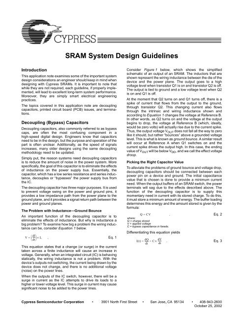
SRAM System Design Guidelines
SRAM System Design Guidelines
SRAM System Design Guidelines

Create successful ePaper yourself
Turn your PDF publications into a flip-book with our unique Google optimized e-Paper software.
<strong>SRAM</strong> <strong>System</strong> <strong>Design</strong> <strong>Guidelines</strong>IntroductionThis application note examines some of the important systemdesign considerations an engineer should keep in mind whendesigning with Cypress <strong>SRAM</strong>s. It is important to note thatwhile they are not required, each guideline, if properly implemented,will lead to excellent long-term system performance.Moreover, they are simply smart electrical engineeringpractices.The topics covered in this application note are decouplingcapacitors, printed circuit board (PCB) issues, and terminations.Decoupling (Bypass) CapacitorsDecoupling capacitors, also commonly referred to as bypasscaps, are often the most confusing component in ahigh-speed digital design. Engineers know that capacitorsneed to be in the design, but the purpose and operation of thepart is often unclear. Additionally, as the speed of signalsincreases, many older designs using the same decouplingmethodology need to be updated.Simply put, the reason systems need decoupling capacitorsis to reduce the amount of noise in the power system. Morespecifically, the goal of this capacitor is to eliminate the effectsof inductance on the power supply bus. Essentially, thecapacitor, which has a low series resistance and series inductance,decouples or “bypasses” the power supply bus fromthe IC.The decoupling capacitor has three major purposes. It is usedto prevent voltage swing on the power and ground pins, itprovides a low impedance path from the power plane to theground plane, and it provides a signal return path between thepower and ground planes.The Problem with Inductance—Ground BounceAn important function of the decoupling capacitor is toeliminate the effects of inductance. But why is inductance abig problem? To examine how big a problem the wiring inductancecan be, consider Equation 1 below.dIV = ⎛----⎞×L⎝dt⎠. Eq. 1This equation states that a change (or surge) in the currenttaken across a finite inductance will cause an increase involtage. Generally, when an integrated circuit (IC) is behavingstatically, the wiring inductance is not a problem. With thedevice’s outputs not switching, the current being drawn by thedevice does not change, and there is no additional voltage(noise) on the power lines.When the outputs of the IC switch, however, there will be asurge in current as the IC attempts to drive its loads to ahigher or lower voltage level. This surge in current may causesignificant noise to be added to the power lines.Consider Figure 1 below, which shows the simplifiedschematic of an output of an <strong>SRAM</strong>. The inductors that areshown represent the wiring inductance between the die of thedevice and the power plane. The output goes to a highvoltage level when transistor Q1 is on and transistor Q2 is off.The output is tied to ground and a low voltage level when Q2is on and Q1 is off.At the moment that Q2 turns on and Q1 turns off, there is aspike of current that flows from the output to the ground,through transistor Q2. This changing current also flowsthrough the intrinsic and wiring inductance shown andaccording to Equation 1 changes the voltage at Reference B.In other words, as Q2 turns on and the voltage at the outputbegins to drop, the voltage at Reference B (which, ideally,would be zero volts) will actually rise due to the current spike.Thus, the output voltage V OUT does not fall all the way to zerolike it should, but rather “bounces” above a grounded voltagelevel. This is what is known as ground bounce. A similar resultwill occur at Reference A when Q1 switches on and thecurrent spike drives the output high. In this case, the endingvalue of V OUT will be below V DD , and we call the effect voltagedroop.Picking the Right Capacitor ValueTo alleviate the problems of ground bounce and voltage drop,decoupling capacitors should be connected between eachpower pin on a device and ground. The initial capacitancevalue that is chosen is done to provide a minimum currentneed. When the output buffers of an <strong>SRAM</strong> switch, the powerterminals will sag due to the effects described above. Thefunction of the decoupling capacitor is to supply thismomentary need in current with its stored charge. To do this,it must store a minimum amount of energy. The buffer loadingdetermines this energy and the amount stored is given by theformula:Q = CV. Eq. 2where:Q = charge storedV = applied voltageC = bypass capacitance in farads.Differentiating this equation yieldsIt () =dQ------ = C ×dV ------dt dt. Eq. 3Cypress Semiconductor Corporation • 3901 North First Street • San Jose, CA 95134 • 408-943-2600October 25, 2002
<strong>SRAM</strong> <strong>System</strong> <strong>Design</strong> <strong>Guidelines</strong>V DDOutput BufferQ1Q2Ref ARef BOutputThis is important in understanding what happens during theoperation of a capacitor. Consider Figure 3, which shows thebehavior of two ideal components, a capacitor and aninductor, which represent the reactive parts of the capacitorshown in Figure 2. Note that without any lead inductance orresistance, the resulting capacitive reactance approaches 0Ωwith increasing frequency. Note also that the inductivereactance of the ideal inductor, without any stray capacitance,approaches infinity.GNDFigure 1. Effects of Ground BounceThis equation allows us to calculate the capacitance requiredto prevent the voltage drops due to the switching outputdrivers. For example, suppose we have an <strong>SRAM</strong> witheighteen 3.3V output drivers driving a 50-ohm trace with arise and fall time of 3 ns. Let us also assume that a voltagedrop of 300 mV is the maximum amount of voltage dropallowable to the component.First, we need to calculate the output current during the riseof the clocks. Assuming the outputs reach 3V, each outputrequires 3V/50 ohm = 60 mA. Because the <strong>SRAM</strong> haseighteen such drivers, the total current required is 1080 mA.Solving for C in Equation 3 above yieldsdtC = I×------dV3nsC = 1080mA× ----------------- = 0.0108µF300mV. Eq. 4This suggests that this amount of total capacitance is requiredon the component to maintain less than 300 mV of voltageswing. Often, 0.1-µF capacitors are used for bypassing.Another way to view this situation is to say that a 0.1-µFcapacitor supplies 1080 mA of instantaneous current in 3nswith only 32.4 mV of voltage swing across the bypasscapacitor.This example assumed a worse-case scenario voltage swingon the outputs of 3V. Depending on the termination methodused, this swing could be less than this amount. However,since this is used only as a guide, it is best to overestimatethe value.Capacitor FilteringWe have seen that the main role of decoupling capacitors isto block unwanted noise going onto and coming from thepower plane. It should be noted, however, that decouplingcaps are much more than a capacitor. Since capacitorsalways have a finite, intrinsic resistance and inductance, theyare, in effect, a capacitor in series with an inductor and aresistor, as shown in Figure 2 below.Figure 2. Capacitor ModelFigure 3. Z vs. f for Parts of a Real CapacitorThe impedance curve of “Real” capacitors resembles thetraces marked 22 nF and 100 pF of Figure 4. The shape ofthese calculated curves match those found in a capacitormanufacturer’s data sheets. This means that, in a circuit, acapacitor acts as a low-impedance element only over alimited range of frequencies. To extend this frequency range,many references propose adding a second capacitor tobypass frequencies outside the limited range of the singlecapacitor. This approach expects a resulting impedancecurve like the solid line marked “Expected” in Figure 4. Thissolution, however, is not mathematically sound and has asignificant problem at “intermediate” frequencies.What actually happens when two capacitors of differentvalues are in parallel is shown in Figure 5. Notice the spike inimpedance just above 100 MHz. The goal of obtaining lowerimpedance across a wider frequency is not achieved. On thecontrary, the impedance has actually increased in someareas. Therefore, the practice of using two different valuedcapacitors to decouple a power supply bus is not recommended.But, there is a method that will help to lower the impedanceacross all frequencies. When two capacitors of the samevalue and package size are in parallel with each other, nopeak increase in impedance is realized. However, they dohave the effect of halving the inductance. This is a recommendedpractice, however it may be constrained by availableboard space.2
<strong>SRAM</strong> <strong>System</strong> <strong>Design</strong> <strong>Guidelines</strong>Figure 4. Expected Impedance of “Real” CapacitorsFigure 5. Real Z vs. f for Parallel 22-nF and 100-nF Capacitors3
<strong>SRAM</strong> <strong>System</strong> <strong>Design</strong> <strong>Guidelines</strong>What Frequencies to BypassIt is a common misconception that faster clock rates lead tothe need for higher frequency decoupling. This is only partlytrue. Because the frequencies have increased, thetechnology for high-speed memories has been driven toprovide faster rise and fall times. Therefore, a signal whosefrequency is 1 MHz will need the same decoupling as a clockrunning at 50 MHz using the same high-speed buffers. Thedifference may be that there is more timing margin affordedin the slower speed system. A rough generalization suggeststhat frequencies up to one half the fastest signal transitionrate (rise or fall) frequency need to be bypassed:f BYPASS = 0.5/Transition Rate.It should be noted that decoupling is really a four-part systemcomprising the power supply, bulk capacitors, decouplingcapacitors, and intrinsic capacitance in the board. Eachprovides decoupling in its respective frequency bands withthe power supply addressing the very low frequencies and theintrinsic board capacitance addressing the high frequencies.The difference between the capacitance is large enoughbetween each part that the large spiking effect with multiplecapacitor value interaction explained above does not occur.However, between each frequency band there will be smallpeaks. These peaks will always exist but they can be movedslightly.Generally, engineers have limited ability to alter the characteristicsof the power supply and board plane capacitance.But it is possible to vary the bulk and decoupling capacitancevalues. The goal is to have the four-part system provide a lowimpedance path (less than 1 ohm) throughout the frequencyrange. By adjusting the values of the decoupling capacitors,the small impedance peaks can be shifted to allow for thelowest impedance in the frequency ranges of concern.Decoupling Capacitors: <strong>Design</strong> RecommendationsAs we have now seen, decoupling capacitors play a huge rolein how well the <strong>SRAM</strong> performs. Along with appropriatelypicking the right value capacitor, connecting them on theboard is of extreme importance in terms of performance.Generally, a PCB should be designed to keep wiring and leadinductances as low as possible. Long, narrow PCB tracesshould be avoided because they increase inductance.Passing through a via is acceptable provided the path is lowerinductance than an alternative longer trace. The following isa list of rules when designing with decoupling capacitors.1. Use only one value capacitor for the component.2. Keep decoupling capacitors as close to the component aspossible.3. Use a minimum of one capacitor on each power pin.4. Keep capacitors on the same side of the board as thecomponent, if possible.5. Minimize the lead and wiring inductance.6. Ensure that the capacitor value meets the voltage swingrequirements, and that it provides a low-impedance pathto ground in the intended frequency range of the application.PCB Layout ConsiderationsThe PCB provides two significant functions in an electricaldesign: mechanical locations for the components that resideon the board, and connectivity between components. Theseconnections play an important role in providing a solidpathway to the power system and ensuring the highestdegree of signal integrity.The traces and planes that comprise a printed circuit boardcan be separated into two categories. There are pathways forthe power source and there are traces required to carry theactual signals. This section of the application note willexamine how both of these directly affect system integrity.Power and Ground PlanesPower planes are large sheets of a conductive material thattypically reside on entire PCB layers. They provide fourprimary functions to the circuit. They are:1. a low-impedance path for power from its source to thecomponents on the PCB.2. a physical channel to vent and move heat from the components.3. electrostatic shielding between the electromagnetic fieldsof signal traces that run on both sides of the planes.4. a sheet capacitance for the ground plane that exists onother layers of the PCB. This in turn provides additional ACbypassing within the power circuitry of the PCB.The primary functionality of a power plane is to reduce theresistance that causes a voltage drop between componentand power source. The thickest power plane available willprovide the best results. For example, using a two-ouncecopper power plane instead of a one-ounce will cut in half anypoint-to-point path resistance. It can be thought of as havingtwo resistors (and inductors) in parallel. The increased planethickness reduces both the DC resistance and AC inductancedrops. The drop in DC resistance allows the power supply toreach the component cleanly, while the reduction in AC inductanceprovides a low-impedance path for signal returncurrents.As a secondary benefit, the thicker plane also increases theability to sink heat out of the component. The bond wires andlead frames are a major thermal path in non-heat-sinkedcomponents.The planes also aid in the reduction of electromagnetic interference(EMI). They provide a lower-impedance path acrosswhich the EMI develops and a larger faraday shield to shortout these radiated fields.The sheet capacitance that the power plane provides isproportional to its size, its distance from the ground plane,and the dielectric constant of the material between them. Ithas the benefit of providing bypass capacitance, particularlyat the high frequencies. While it is far from being sufficient toprovide all of the bypassing needs of a high-speed logicdesign, it should be utilized to its maximum. The capacitanceof the planes can be calculated by the following equation:4
<strong>SRAM</strong> <strong>System</strong> <strong>Design</strong> <strong>Guidelines</strong>C = 0.225E R ([( N–1) × A] ⁄ t)where:E R = The relative dielectric constantN = Number of platesA = Area of one side of one plate in square inchest = Thickness (separation of plates) in inches. Eq. 5For example, using a 10-inch by 10-inch FR-4 board with anE R of 4.1 and 0.005-inch separation between the power andground plane, the capacitance is calculated asC = 0.225( 4.1) ([( 2–1) × 100] ⁄ 0.005) = 18,450pF.Eq. 6This is equivalent to 184 pF per square inch. Table 1 showsthe dielectric constants for several common materials used inPCB design today. It is always advisable to consult your fabricatorfor the precise ER value, since different epoxies areused when constructing a PCB. Dielectric constants of PCBsalso change with frequency, as shown in Table 1.Table 1. Dielectric ConstantsMaterialE R@ 1 MHz @ 300 MHzFR-4, Tetra Functional 4.2 – 4.6 4.0 – 4.3FR-4, High-grade Multifunctional 4.2 – 4.6 4.1 – 4.4Polyimide 4.2 – 4.6 4.1 – 4.3GETEK 3.9 – 4.1 3.9 – 4.0BT 3.6 – 4.1 3.55 – 4.0CE 3.6 – 4.0 3.6 – 4.0ViasVias are commonly used to connect the power plane to thepower traces that ultimately attach to the power pins of thecomponents. They can also have an impact on the powersignal quality.First, vias produce a higher resistance than a copper trace.This is due to the material typically used in the fabrication ofthe via, which is plated granular copper. The resistance of avia changes based on the thickness of the copper that isplated in the via hole. Therefore, larger vias have a lower DCresistance and hence develop less of a DC voltage drop forany given current.Vias also add inductance to the power trace. This inductancecauses high-frequency noise that is present on the powerplane to stay on the plane (which is good), but it also isolatesthe capacitance effect of the power plane from the componentson the other ends of the vias. Filling vias with solder,using heavy plating, enlarging their size and using multiplevias per power connection are the preferred methods oflowering both the resistive and inductive parasitic effects theyhave on power connections.Power TracesSimilar to vias, a trace also has some amount of resistance,capacitance, and inductance. The overall resistance must bekept to a minimum to avoid voltage drop on the trace. For thepower plane to reach the power trace and ultimately thecomponent, a via is also required.If connections to the device are made in correct sequence,the resistance and inductance of the trace and via will isolatethe component’s noise from passing into the power plane.This effect increases as the frequency of the noise rises. Toachieve this isolation, the power trace must pass from the viato the decoupling capacitors pad and then to the component.This order is important to create an island of protected tracebetween the decoupling capacitor and the component.It is important to highlight that the trace between componentand bypass capacitor be as short as possible. As we havementioned, the goal is to keep the inductance between thedevices to a minimum. A short, wide trace will produce betterresults than a long, narrow trace.Signal Return PathsThe power planes play a key role in the return currents ofhigh-speed digital signals. At very slow speeds, the returncurrent follows the path of least resistance. At higher speeds,however, the return currents follow the path of least inductance.This can be on either power or ground plane, directlybelow the signal trace. Normally, the return path is on theground plane on standard PCB designs. When the returncurrent reaches the driving component, the decouplingcapacitors provide the bridge to the proper voltage plane.In order to maintain good signal integrity and to minimizecrosstalk, a clean, unobstructed return path needs to beprovided. For example, if a return signal encounters a 5-ohmtrace within the ground plane, the integrity of the normalsignal on the 50-ohm trace can be compromised.There are a few simple rules to follow for planes. First, itshould be as continuous as possible. By placing excessiveclearances around holes that pass through, it may make fabricationeasier but it can cause the return current to travelthrough a non-optimal path. The effect of the clearance holesshould be analyzed. Second, cutouts in the ground planemust be avoided. Similar to the clearance holes for the vias,a ground plane cutout will force the return path current aroundthe cutout if the signal trace crosses above the cutout. Thiswill increase the inductance of the path and decrease the risetime of the digital signal on the trace. It will also increase thepotential for crosstalk.CrosstalkCrosstalk can exist between traces on a PCB. If this occurson a memory signal with sufficiently strong amplitude, a falsetrigger can occur. Crosstalk should therefore be minimized inthe design.As a signal travels through a trace, it creates a magnetic field.It also reacts to other magnetic fields within its path. Thesemagnetic fields have adverse effects on digital signals sincethey create unwanted noise on other signals. This effect isknown as crosstalk. The voltages that external fields causeare proportional to the strength of the external fields and thelength of the trace that is exposed to the field. Often, the tracethat causes the crosstalk is termed the “source” or“aggressor,” and the trace that is affected first is called the“victim.”Crosstalk between traces is a function of both mutual inductanceand mutual capacitance. A model of inductance andcapacitance between traces is shown in Figure 6. Itsmagnitude is proportional to the distance from the sourcetrace, the speed of the signal edge rate, and the impedanceof the victim trace. In digital systems, crosstalk caused bymutual inductance is typically equal to or larger than thecrosstalk associated with mutual capacitance.5
SourceTraceLInductiveCoupling(L M )CapacitiveCoupling(C M )VictimTraceLFigure 6. Mutual Coupling Between TracesTo illustrate the effects of spacing, the mutual inductance L Mcan be calculated with the following equation:LLM = -----------------------⎛ s1 + --⎝ ⎝ ⎛ h⎠⎞2 ⎞⎠where:L = Inductance of the wires = separation between the wiresh = height above the plane. Eq. 7Figure 8. Crosstalk versus Impedance and SpacingThis shows that moving the traces away (value s) from eachother or by moving the traces closer (value h) to the plane,the mutual inductance is reduced by the square of the charge.And, since crosstalk is proportional to the mutual inductance,the magnitude of the crosstalk is also reduced. Figure 7below illustrates this model.STrace AWHGround PlaneFigure 7. Trace and Ground PlanesTrace BThe mutual capacitance C M injects current I M into the victimtrace and can be calculated as:dVsI M = C M × ---------dt. Eq. 8where:dVs = Vs is the source voltageFigure 8 illustrates the effects of trace impedance oncrosstalk coupling. The higher the impedance of the victimtrace, the more susceptible it is to noise from crosstalk.Figure 9 shows a similar effect but with varying the width ofthe trace line. Wider traces produce less crosstalk coupling.Therefore, minimum coupling is created with maximumspacing, maximum trace widths, and minimum impedance.To minimize the effects of magnetic field coupling, three basicrules should be followed.First, separate the traces with more distance. The effect thatis seen is directly proportional to the square of the distance ofthe elements and therefore doubling the distance will reducethe coupling by a factor of four.Figure 9. Crosstalk versus Width and SpacingThe second method of decreasing the coupling is to shield thetarget trace. Either routing it on another layer or placingprotective guard traces between the two does this. In this waythe magnetic lines will have a portion of their energydeveloped in the protective traces, usually at groundpotential, and the field that cuts across the trace beingshielded is less.A third way to reduce the impact of crosstalk is to use differentialsignaling. This type of signal rejects noise fromcrosstalk if both true and complement signals are equallyaffected. This is commonly called common-mode noiserejection. However, if the crosstalk affects one trace of thedifferential pair and not the other, noise coupling can be afactor.LayersIn order to keep noise at a minimum and to achieve the bestin signal integrity, control of the PCB layers is required.As was mentioned above, spacing power and ground planesclose together gains additional bypassing capacitance. Ofmore importance is the creation of a reference plane thatprovides constant trace impedance. The reference plane isusually the ground plane. The thickness of the substratebetween controlled impedance traces and the ground planemust be selected to be both manufacturable and able to keepthe desired characteristic trace impedance within acceptablelimits. As the spacing of layers decreases, the ability to holdtight, repeatable spacing value decreases. A 1-mil variationon a 10-mil spacing is 10% and on a 20-mil spacing it is only5%. You should consult with your manufacturer on the tolerances.
<strong>SRAM</strong> <strong>System</strong> <strong>Design</strong> <strong>Guidelines</strong>When power planes are correctly bypassed, they are at thesame AC potential as ground planes. Therefore, they can beused as a reference for controlled impedance traces. Usingboth power and ground planes, however, is unwise becausethe transition between the two has a high potential of causingnoticeable impedance discontinuities in trace impedance,which is a source of unwanted reflections. (This applicationnote will explain reflections in more detail in the next section.)Vias in TracesWhen routing a trace, the signal should remain on the samesignal plan. Using a via to route to another plane diminishessignal quality. Vias should therefore be avoided as much aspossible. If vias have to be used in a high-speed design, thefollowing guidelines should be considered.1. Make vias as large as possible (more area equals lessinductance and resistance).2. Plate external layers with the maximum thickness ofcopper during fabrication.3. Plating of filling the via holes solid.+ _Distance(Y-X)XYStep Voltage: VAt point X, the step is still ofsize V, but is now delayedAt point Y, the step isdelayed even furtherReflections and TerminationsAnother problem that arises in digital signal systems involvesreflections due to poorly terminated transmission lines. Thissection will discuss a few important points to remember whendesigning with long wiring networks. For a full discussion ontransmission lines, please refer to the Terminations applicationnote available on the Cypress web site.What is a Reflection?A reflection is an unwanted pulse on a transmission line thatis a result of an unmatched source or load impedance. Thetransmission line has an intrinsic value called its characteristicimpedance. A reflection back toward the driver sourcecan occur if the line’s load and characteristic impedances arenot matched, and a second reflection back toward the loadcan occur if the source and characteristic impedances arealso not matched.Why do Reflections Occur?Reflections occur because of impedance mismatches thatcause a disproportion of energy transfer. If the line is ideal,and the source impedance Z S equals the load impedance Z L ,then half the energy in the propagating signal will be lost inthe source impedance, and the other half in the loadimpedance (since the ideal line is lossless). However, if theload resistor at the end of the line is larger than the line’scharacteristic impedance, there will be extra energy availablethat is “reflected” back toward the source. That is, there isanother signal that propagates down the line that “bounces”off the load if there is an impedance mismatch.Characteristic ImpedanceThe most important variable of any line is its characteristic, orinput, impedance. This is the impedance seen looking into thetwo left-hand terminals of the line.t 0 t 1Figure 10. Voltage Step Input to an Ideal LineFigure 10 below illustrates how a digital pulse propagatesdown an ideal line. The pulse is set onto the beginning of theline by the source at time t = 0. This pulse is then transferreddown the line without being distorted or attenuated while it isdelayed in time according to the line’s propagation delay. Atpoint X, the voltage on the line is low, until time t 0 at whichtime the signal passes point X on the line, and we can seethat the pulse drives the voltage up to the high level. A similarsituation exists for point Y, except that the signal stays lowlonger while it waits for the pulse to propagate down the line.We can find the characteristic impedance of this line byfinding the amount of current it takes to impress the stepvoltage on a given length of the line, in this case betweenarbitrary points Y and X.The capacitance of the length of line between points X and Yis given as:CC xy = ⎛----⎞×( Y–X)⎝in·⎠. Eq. 9The total additional charge necessary to charge the capacitancebetween these points is equal to:CCharge= C xy= ⎛----⎞ ⎝in·⎠ ( Y–X)V. Eq. 10The time interval (in seconds) in which during which Cxy mustbe charged is equal to the separation of the two points timesthe propagation delay in seconds per unit length:T = ( Y–X)⎛----L⎞⎛----C⎞⎝in·⎠⎝in·⎠. Eq. 117
<strong>SRAM</strong> <strong>System</strong> <strong>Design</strong> <strong>Guidelines</strong>The average current supplied is equal to the total chargesupplied divided by the length of time T:⎛C----⎞ ( Y–X)VCharge ⎝in·⎠I = ---------------- = ----------------------------------------TL( Y–X)⎛----⎞⎛----C⎞⎝in·⎠⎝in·⎠. Eq. 12This gives us the current flow required to sustain a propagatingstep edge of V volts. Therefore, the characteristicimpedance of an ideal line can be found through simplificationZ o =V--- = ---LEq. 13I Cwhere L and C are given in per-unit lengths.As this equation shows, the value of characteristic impedancefor ideal lines is real-valued, constant, and dependent only onthe inductance and capacitance of the line-per-unit length.This allows us to model a transmission line as a simpleresistor.The characteristic impedance equation given above for anideal line does not depend on the frequency of the system.This is not the case for a lossy line, however. The generalformula for characteristic impedance is given asV R+jωLZ o = --- = ----------------- . Eq. 14I jωCThis is the impedance if a finite value of resistance exists.Note that Z o is actually a function of frequency. However,since digital signals operate at very high frequency alongPCB traces that have very low resistance, it is simpler to usethe form given in Equation 10.Termination StrategiesThe end goal of all termination strategies is to remove voltagereflection on the line by cancelling out the two voltagereflection coefficients. There are two general strategies fordoing this:1. match the load impedance to the line’s characteristic impedance.2. match the source impedance to the line’s characteristicsimpedance.Under one of these conditions, the load or source reflectioncoefficient will be made to equal zero and thus there will beno reflection. If the load is matched, there will be no reflectionback to the source, and if the source is matched, thisreflection will not bounce back again toward the load.Matching the load is slightly preferred, since eliminating thefirst reflection will reduce EMI and electrical noise, and also itseems logical to try and eliminate any reflections as soon asone might occur.approved kkv 10/__/02© Cypress Semiconductor Corporation, 2002. The information contained herein is subject to change without notice. Cypress Semiconductor Corporation assumes no responsibility for the useof any circuitry other than circuitry embodied in a Cypress Semiconductor product. Nor does it convey or imply any license under patent or other rights. Cypress Semiconductor does not authorizeits products for use as critical components in life-support systems where a malfunction or failure may reasonably be expected to result in significant injury to the user. The inclusion of CypressSemiconductor products in life-support systems application implies that the manufacturer assumes all risk of such use and in doing so indemnifies Cypress Semiconductor against all charges.