Tech Talk Fine Lines in High Yield (Part CXLIX) Opens and ... - DuPont
Tech Talk Fine Lines in High Yield (Part CXLIX) Opens and ... - DuPont
Tech Talk Fine Lines in High Yield (Part CXLIX) Opens and ... - DuPont

Create successful ePaper yourself
Turn your PDF publications into a flip-book with our unique Google optimized e-Paper software.
<strong>Tech</strong> <strong>Talk</strong><br />
<strong>F<strong>in</strong>e</strong> <strong>L<strong>in</strong>es</strong> <strong>in</strong> <strong>High</strong> <strong>Yield</strong> (<strong>Part</strong> <strong>CXLIX</strong>)<br />
<strong>Opens</strong> <strong>and</strong> Shorts<br />
Karl H. Dietz (for CircuiTree Magaz<strong>in</strong>e, February, 2008)<br />
Karl Dietz is the manager at <strong>DuPont</strong>'s<br />
Electronic Materials Laboratory,<br />
Research Triangle Park, NC. His<br />
responsibilities <strong>in</strong>clude application<br />
studies for pr<strong>in</strong>ted circuit materials. Karl<br />
has 35 years of experience <strong>in</strong> a variety of<br />
R&D, manufactur<strong>in</strong>g <strong>and</strong> quality control<br />
functions <strong>and</strong> holds a PhD. <strong>in</strong> organic<br />
chemistry from the University of Frankfurt,<br />
Germany. If you would like to participate<br />
<strong>in</strong> the exchange or if you have any<br />
questions, Karl Dietz can be reached at<br />
919-248-5248, fax: (919) 248-5132, or via<br />
e-mail .<br />
All PWBs, modules, <strong>and</strong> IC packages<br />
consist of conductive features (circuit<br />
l<strong>in</strong>es, vias, pads, power <strong>and</strong> ground<br />
etc) <strong>in</strong>sulated from each other by non-conductive<br />
(dielectric) material. Therefore, all<br />
defects orig<strong>in</strong>at<strong>in</strong>g <strong>in</strong> the circuitiz<strong>in</strong>g process<br />
steps essentially consist of not hav<strong>in</strong>g <strong>in</strong>sulation<br />
where it is required (“short”) or hav<strong>in</strong>g an<br />
<strong>in</strong>sulat<strong>in</strong>g <strong>in</strong>terruption <strong>in</strong> the conductive path<br />
(“open”), <strong>and</strong> a number of defects that br<strong>in</strong>g<br />
us dangerously close to hav<strong>in</strong>g opens or<br />
shorts such as space violations, copper spots<br />
(extraneous copper), m<strong>in</strong>imum l<strong>in</strong>e width<br />
violations, or dish-downs.<br />
Scope of this Overview<br />
The “column”-format of <strong>Tech</strong> <strong>Talk</strong> does not<br />
lend itself to an <strong>in</strong>-depth review of open <strong>and</strong><br />
short defects, <strong>in</strong>clud<strong>in</strong>g assignment of root<br />
causes, troubleshoot<strong>in</strong>g guidel<strong>in</strong>es, <strong>and</strong><br />
corrective actions. This column will only focus<br />
on open <strong>and</strong> short defects associated with<br />
photoresist. An example of a review of open<br />
<strong>and</strong> short defects with a different focus is<br />
Michael Barbetta’s (Ref. 1) <strong>in</strong>vestigation of<br />
r<strong>and</strong>om opens <strong>and</strong> shorts due to dirt that<br />
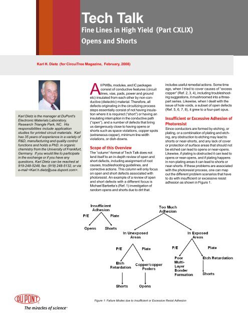
Figure 1: Failure Modes due to Insufficient or Excessive Resist Adhesion<br />
<strong>in</strong>cludes useful remedial actions. Some time<br />
ago, when I tried to cover causes of “excess<br />
copper” (Ref. 2, 3, 4), <strong>in</strong>clud<strong>in</strong>g troubleshoot<strong>in</strong>g<br />
suggestions, it mushroomed <strong>in</strong>to a threepart<br />
series. Likewise, when I dealt with the<br />
issue of hole voids, a subset of open defects<br />
(Ref. 5, 6, 7, 8), it grew to a four-part opus.<br />
Insufficient or Excessive Adhesion of<br />
Photoresist<br />
S<strong>in</strong>ce conductors are formed by etch<strong>in</strong>g, or<br />
plat<strong>in</strong>g, or a comb<strong>in</strong>ation of plat<strong>in</strong>g <strong>and</strong> etch<strong>in</strong>g,<br />
any obstruction to etch<strong>in</strong>g may lead to<br />
shorts or near-shorts, <strong>and</strong> any lack of cover<br />
or protection of surface areas that should not<br />
be etched can lead to opens or near-opens.<br />
Likewise, if plat<strong>in</strong>g is obstructed it can lead to<br />
opens or near-opens, <strong>and</strong> if plat<strong>in</strong>g happens<br />
<strong>in</strong> non-plat<strong>in</strong>g areas it can lead to shorts or<br />
near-shorts. If these problems are associated<br />
with the photoresist process, one can map<br />
out the different problem scenarios that have<br />
to do with <strong>in</strong>sufficient or excessive resist<br />
adhesion as shown <strong>in</strong> Figure 1.
The failure mechanisms due to “Insufficient<br />
Adhesion” are pretty obvious: <strong>in</strong> the pr<strong>in</strong>t &<br />
etch (P&E) process there is the danger of<br />
under-etch<strong>in</strong>g the resist which will lead to<br />
opens or near-opens such as mouse bites or<br />
dish-downs. In the plat<strong>in</strong>g process there is the<br />
possibility of under-plat<strong>in</strong>g so that after<br />
copper plat<strong>in</strong>g, metal etch resist plat<strong>in</strong>g <strong>and</strong><br />
resist stripp<strong>in</strong>g, we have to etch through more<br />
copper where under-plat<strong>in</strong>g occurred, <strong>and</strong><br />
s<strong>in</strong>ce the etch<strong>in</strong>g process has been set up <strong>in</strong><br />
such a way that there is just enough etch<strong>in</strong>g<br />
to remove the base copper <strong>and</strong> the th<strong>in</strong><br />
electroless copper, there will not be enough<br />
time <strong>in</strong> the etcher to remove the excessive<br />
copper thickness <strong>in</strong> the under-plated area.<br />
The failure mechanisms due to “Too Much<br />
Adhesion” are more complex as is evident<br />
from Figure 1. One has to dist<strong>in</strong>guish between<br />
too much adhesion <strong>in</strong> unexposed areas <strong>and</strong><br />
too much adhesion <strong>in</strong> exposed areas. Too<br />
much adhesion <strong>in</strong> unexposed areas <strong>in</strong> the P&E<br />
process will leave development residues on<br />
top of the copper that is to be etched. This<br />
can lead to etch retardation which <strong>in</strong> turn can<br />
lead to shorts or near-shorts. Too much<br />
adhesion <strong>in</strong> unexposed areas <strong>in</strong> the plat<strong>in</strong>g<br />
process can leave resist residues <strong>in</strong> the area<br />
where plat<strong>in</strong>g should occur. Such residues<br />
may impede plat<strong>in</strong>g altogether or, if plat<strong>in</strong>g<br />
occurs, the resist residues don’t allow the<br />
plated copper to bond tightly to the base<br />
copper which may lead to copper/copper<br />
peelers, <strong>and</strong> ultimately to opens. If there is too<br />
much adhesion <strong>in</strong> the exposed resist areas,<br />
this may lead to resist residues <strong>in</strong> the P&E<br />
process after stripp<strong>in</strong>g on top of the copper<br />
circuit which can <strong>in</strong>terfere with the application<br />
of the multilayer bonder treatment which <strong>in</strong><br />
turn may lead to lam<strong>in</strong>ation defects. If there is<br />
too much adhesion of the exposed resist <strong>in</strong><br />
the plat<strong>in</strong>g process, there may be resist<br />
residues after stripp<strong>in</strong>g <strong>in</strong> areas that should<br />
be etched which can lead to etch retardation<br />
<strong>and</strong> shorts between plated l<strong>in</strong>es.<br />
Causes of Insufficient Resist<br />
Adhesion<br />
Poor resist adhesion is typically associated<br />
with <strong>in</strong>adequate surface preparation or faulty<br />
lam<strong>in</strong>ation conditions. Lack of adhesion due to<br />
<strong>in</strong>adequate surface preparation can be<br />
caused by <strong>in</strong>sufficient copper micro-roughness<br />
or organic contam<strong>in</strong>ation (see Ref. 9) or<br />
by excessive chromate residues (see Ref. 10,<br />
11). Poor resist adhesion due to lam<strong>in</strong>ation<br />
problems may be caused by low lam<strong>in</strong>ation<br />
pressure, low lam<strong>in</strong>ation temperature, or fast<br />
lam<strong>in</strong>ation speed. Under-exposure is another<br />
potential cause for poor adhesion. One should<br />
also keep <strong>in</strong> m<strong>in</strong>d that not all resists are<br />
formulated to adhere to copper through nickel<br />
<strong>and</strong> gold plat<strong>in</strong>g or alkal<strong>in</strong>e etch<strong>in</strong>g.<br />
Causes of Excessive Resist Adhesion<br />
This problem is less prevalent than <strong>in</strong>sufficient<br />
resist adhesion. It may be due to high lam<strong>in</strong>ation<br />
temperature, long post-lam<strong>in</strong>ation hold<br />
times, or it could happen with wet lam<strong>in</strong>ation<br />
of a dry film resist that is not compatible with<br />
wet lam<strong>in</strong>ation.<br />
Other Resist Related Causes for<br />
<strong>Opens</strong> or Shorts<br />
The failure mechanisms described under<br />
“Insufficient Adhesion” are of course not only<br />
applicable for the case of <strong>in</strong>sufficient adhesion<br />
of the resist, but also apply to poor resist<br />
conformation (<strong>in</strong>terfacial voids), <strong>and</strong> to the<br />
case were resist had good adhesion but was<br />
mechanically removed due to h<strong>and</strong>l<strong>in</strong>g damage.<br />
In addition, it applies to the situation<br />
where the questionable area was never<br />
covered by resist due to a flaw <strong>in</strong> the phototool,<br />
e.g. opaqueness <strong>in</strong> the clear area of the<br />
phototool, or an obstruction to exposure due<br />
to dirt <strong>in</strong> the exposure unit, scratches <strong>in</strong> the<br />
exposure frame etc. Last not least, the<br />
phototool may have been perfect, the exposure<br />
unit spotless, but the exposure energy<br />
was set too low. In this case we have resist<br />
where we expect it to be, but it may not<br />
survive the development process.<br />
Over-development could be a cause of shorts<br />
or near-shorts. This is due to developer attack<br />
on the resist sidewall which can lead to a<br />
positive resist foot, or more likely to resist<br />
slivers break<strong>in</strong>g off the “nose” of the resist<br />
sidewall <strong>and</strong> re-deposit<strong>in</strong>g on the board<br />
surface. Re-deposition of resist may also<br />
have other causes. Tacky, partially polymerized<br />
resist, e.g. orig<strong>in</strong>at<strong>in</strong>g from the use of<br />
step tablets, may get stuck to transport rollers<br />
from where it transfers to the board surface.<br />
Poor filtration <strong>in</strong> the developer can cause an<br />
accumulation of resist particles <strong>in</strong> the development<br />
chamber, <strong>and</strong> may lead to resist particles<br />
be<strong>in</strong>g pressed onto the board by exit squeegee<br />
rollers. Unwanted resist residues on the<br />
board surface that don’t get removed <strong>in</strong> the<br />
stripper can cause shorts <strong>in</strong> pattern plat<strong>in</strong>g.<br />
This problem can occur if boards are overplated<br />
(“mushroomed”) or with very f<strong>in</strong>e l<strong>in</strong>es<br />
<strong>and</strong> spaces. In the latter case the use of<br />
resist that dissolves or partially dissolves <strong>in</strong><br />
the stripper <strong>and</strong> the use of am<strong>in</strong>e-based<br />
proprietary strippers are recommended.<br />
References<br />
1. Reduc<strong>in</strong>g <strong>Opens</strong> <strong>and</strong> Shorts, Michael<br />
Barbetta, CircuiTree Magaz<strong>in</strong>e,<br />
December 2006, pg. 10<br />
2. <strong>F<strong>in</strong>e</strong> <strong>L<strong>in</strong>es</strong> <strong>in</strong> <strong>High</strong> <strong>Yield</strong>s, (<strong>Part</strong> LXXVIII):<br />
Problems with Residual, Excess Copper<br />
<strong>in</strong> Pr<strong>in</strong>t/Etch <strong>and</strong> Tent/Etch Processes<br />
(<strong>Part</strong> A), Karl H. Dietz, CircuiTree<br />
Magaz<strong>in</strong>e, March 2002, pg. 90<br />
3. <strong>F<strong>in</strong>e</strong> <strong>L<strong>in</strong>es</strong> <strong>in</strong> <strong>High</strong> <strong>Yield</strong>s, (<strong>Part</strong> LXXIX):<br />
Problems with Residual, Excess Copper<br />
<strong>in</strong> Pr<strong>in</strong>t/Etch <strong>and</strong> Tent/Etch Processes<br />
(<strong>Part</strong> B), Karl H. Dietz, CircuiTree<br />
Magaz<strong>in</strong>e, April 2002, pg. 40<br />
4. <strong>F<strong>in</strong>e</strong> <strong>L<strong>in</strong>es</strong> <strong>in</strong> <strong>High</strong> <strong>Yield</strong>s, (<strong>Part</strong> LXXX):<br />
Problems with Residual, Excess Copper<br />
<strong>in</strong> Pr<strong>in</strong>t/Etch <strong>and</strong> Tent/Etch Processes<br />
(<strong>Part</strong> C), Karl H. Dietz, CircuiTree<br />
Magaz<strong>in</strong>e, May 2002, pg. 22<br />
5. <strong>F<strong>in</strong>e</strong> <strong>L<strong>in</strong>es</strong> <strong>in</strong> <strong>High</strong> <strong>Yield</strong>s, (<strong>Part</strong> CXIV) :<br />
“Hole Voids” (<strong>Part</strong> A), Karl H. Dietz,<br />
CircuiTree Magaz<strong>in</strong>e, March 2005, pg.<br />
62<br />
6. <strong>F<strong>in</strong>e</strong> <strong>L<strong>in</strong>es</strong> <strong>in</strong> <strong>High</strong> <strong>Yield</strong>s, (<strong>Part</strong> CXV) :<br />
“Hole Voids” (<strong>Part</strong> B), Karl H. Dietz,<br />
CircuiTree Magaz<strong>in</strong>e, April 2005, pg. 50<br />
7. <strong>F<strong>in</strong>e</strong> <strong>L<strong>in</strong>es</strong> <strong>in</strong> <strong>High</strong> <strong>Yield</strong>s, (<strong>Part</strong> CXVI) :<br />
“Hole Voids” (<strong>Part</strong> C), Karl H. Dietz,<br />
CircuiTree Magaz<strong>in</strong>e, May 2005, pg. 54<br />
8. <strong>F<strong>in</strong>e</strong> <strong>L<strong>in</strong>es</strong> <strong>in</strong> <strong>High</strong> <strong>Yield</strong>s, (<strong>Part</strong> CXVII) :<br />
“Hole Voids” (<strong>Part</strong> D), Karl H. Dietz,<br />
CircuiTree Magaz<strong>in</strong>e, June 2005, pg. 46<br />
9. <strong>F<strong>in</strong>e</strong> <strong>L<strong>in</strong>es</strong> <strong>in</strong> <strong>High</strong> <strong>Yield</strong>s, (<strong>Part</strong> L):<br />
Trends <strong>in</strong> Surface Preparation for<br />
Innerlayers, Karl H. Dietz, CircuiTree<br />
Magaz<strong>in</strong>e, October 1999, pg. 58<br />
10.<strong>F<strong>in</strong>e</strong> <strong>L<strong>in</strong>es</strong> <strong>in</strong> <strong>High</strong> <strong>Yield</strong>s, (<strong>Part</strong> XXIII):<br />
What About the Chromate on the<br />
Copper (<strong>Part</strong> A), Karl H. Dietz,<br />
CircuiTree Magaz<strong>in</strong>e, July 1997, pg. 56<br />
11. <strong>F<strong>in</strong>e</strong> <strong>L<strong>in</strong>es</strong> <strong>in</strong> <strong>High</strong> <strong>Yield</strong>s, (<strong>Part</strong> XXIV):<br />
What About the Chromate on the<br />
Copper (<strong>Part</strong> B), Karl H. Dietz,<br />
CircuiTree Magaz<strong>in</strong>e, August 1997, pg.<br />
64