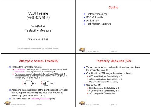
Chapter 3 Testability Measure.pdf
Chapter 3 Testability Measure.pdf
Chapter 3 Testability Measure.pdf

Create successful ePaper yourself
Turn your PDF publications into a flip-book with our unique Google optimized e-Paper software.
VLSI Testing<br />
( 積 體 電 路 測 試 )<br />
<strong>Chapter</strong> 3<br />
<strong>Testability</strong> <strong>Measure</strong><br />
<strong>Testability</strong> <strong>Measure</strong>s<br />
SCOAP Algorithm<br />
An Example<br />
Test Points in Hardware<br />
Outline<br />
Ping-Liang Lai ( 賴 秉 樑 )<br />
Department of Electronic Engineering, Notional Chin-Yi University of Technology<br />
P.L.Lai, VLSI Testing 2010 <strong>Chapter</strong> 3-2<br />
Attempt to Assess <strong>Testability</strong><br />
Test pattern generation requires:<br />
Controllability: controlling a point in the circuit from the primary inputs<br />
Observability: observing the results at primary output<br />
For examples, controlling the output of a multi-input AND gate to 1<br />
requires the control of all its inputs to 1, whereas for an OR gate, it is<br />
sufficient only one of the inputs to 1<br />
1<br />
1<br />
1<br />
1<br />
Assessing the controllability of this point and its observability<br />
can be helpful in determining the ease or difficulty of its<br />
“testability”. (also important to DFT)<br />
Hence the notion of <strong>Testability</strong> <strong>Measure</strong>s (TM)<br />
0<br />
0<br />
1<br />
1<br />
<strong>Testability</strong> <strong>Measure</strong>s (1/3)<br />
Three measures for combinational and another three<br />
for sequential circuits<br />
Combinational TM (major illustration in here)<br />
CC0: Combinational Controllability to 0<br />
CC1: Combinational Controllability to 1<br />
CO : Combinational Observability<br />
Sequential TM<br />
SC0: Sequential Controllability to 0<br />
SC1: Sequential Controllability to 1<br />
SO : Sequential Observability<br />
P.L.Lai, VLSI Testing 2010 <strong>Chapter</strong> 3-3<br />
P.L.Lai, VLSI Testing 2010 <strong>Chapter</strong> 3-4
<strong>Testability</strong> <strong>Measure</strong>s (2/3)<br />
<strong>Testability</strong> <strong>Measure</strong>s (2/3)<br />
<strong>Testability</strong> measures used to get approximate measure of:<br />
Difficulty of setting internal circuit lines to 0 or 1 by setting primary<br />
circuit inputs<br />
Difficulty of observing internal circuit lines by observing primary<br />
outputs<br />
This knowledge can be used to:<br />
Provided analysis of difficulty of testing internal circuit parts, might<br />
require redesigning or addition of special testing hardware<br />
Provides guidance for algorithms performing test pattern generation,<br />
avoid using hard-to-control lines<br />
Provides an estimation of fault coverage<br />
Provides an estimation of test vector length<br />
Controllability: difficulty in setting a particular circuit node to 0 or 1<br />
Observability: difficulty of observing the state of a logic signal<br />
P.L.Lai, VLSI Testing 2010 <strong>Chapter</strong> 3-5<br />
<br />
<br />
<strong>Testability</strong> analysis attributes:<br />
Involves circuit topology analysis, but no test vectors<br />
It has linear complexity, otherwise it is pointless and one might as well<br />
use automatic test pattern generation (ATPG) algorithms<br />
The origin of testability measures is in control theory. Several<br />
algorithms have been proposed:<br />
Rutman 1972: first definition of controllability<br />
Goldstein 1979: SCOAP<br />
<br />
<br />
<br />
» First definition of observability<br />
» First elegant formulation<br />
» First efficient algorithm to compute controllability and observability<br />
Parker and McCluskey 1975: definition of probabilistic controllability<br />
Brglez 1984: COP<br />
» First probabilistic measures<br />
Seth, Pan and Agrawal 1985: PREDICT<br />
» First exact probabilistic measures<br />
P.L.Lai, VLSI Testing 2010 <strong>Chapter</strong> 3-6<br />
<strong>Testability</strong> Analysis - SCOAP<br />
SCOAP Controllability (1/2)<br />
Goldstein's algorithm: SCOAP<br />
We will focus mainly on combinational circuits<br />
<br />
Controllabilities: set Primary Input (PI) controllabilities to 1, progress<br />
from PIs to Primary Outputs (POs), add 1 to account for logic depth<br />
General rules for setting controllabilities<br />
<br />
If only one input sets gate output:<br />
» Output controllability = min (input controllabilites) + 1<br />
If all inputs set gate output:<br />
» Output controllability = sum (input controllabilities) + 1<br />
If gate output is determined by multiple input sets, e.g., XOR:<br />
» Output controllability = min(controllabilities of input sets) + 1<br />
CC0(a), CC1(a)<br />
CC0(b), CC1(b)<br />
a<br />
b<br />
a<br />
b<br />
a<br />
b<br />
a<br />
b<br />
a<br />
b<br />
a<br />
b<br />
z<br />
z<br />
z<br />
z<br />
z<br />
z<br />
CC0(z)=min{(CC0(a), CC0(b)}+1<br />
CC1(z)=CC1(a)+CC1(b)+1<br />
CC0(z)=CC0(a)+CC0(b)+1<br />
CC1(z)=min{(CC1(a), CC0(b)}+1<br />
CC0(z)=min{(CC0(a)+CC0(b), CC1(a)+CC1(b)}+1<br />
CC1(z)= min{(CC1(a)+CC0(b), CC0(a)+CC1(b)}+1<br />
CC0(z)=CC1(a)+CC1(b)+1<br />
CC1(z)=min{(CC0(a), CC0(b)}+1<br />
CC0(z)=min{(CC1(a), CC1(b)}+1<br />
CC1(z)=CC0(a)+CC0(b)+1<br />
CC0(z)=min{(CC1(a)+CC0(b), CC0(a)+CC1(b)}+1<br />
CC1(z)= min{(CC0(a)+CC0(b), CC1(a)+CC1(b)}+1<br />
a<br />
z<br />
CC0(z)=CC1(a)+1<br />
CC1(z)=CC0(a)+1<br />
P.L.Lai, VLSI Testing 2010 <strong>Chapter</strong> 3-7<br />
P.L.Lai, VLSI Testing 2010 <strong>Chapter</strong> 3-8
SCOAP Controllability (2/2)<br />
SCOAP Observability (1/2)<br />
<br />
Combinational Controllability Calculation Rules<br />
<br />
Observabilities: after controllabilities have been computed, set PO observabilities to<br />
0, progress from POs to PIs, add 1 to account for logic depth<br />
0-controllability<br />
(Primary input, output, branch)<br />
1-controllability<br />
(Primary input, output, branch)<br />
<br />
The difficulty of observing a designated input to a gate is the sum of<br />
The output observability<br />
Primary Input 1 1<br />
<br />
<br />
The difficulty of setting all other inputs to non-dominant values<br />
And 1 for the logic depth<br />
AND min {input 0-controllabilities} + 1 Σ(input 1-controllabilities) + 1<br />
OR Σ(input 0-controllabilities) + 1 min {input 1-controllabilities} + 1<br />
NOT Input 1-controllability + 1 Input 0-controllability + 1<br />
CC0(a), CC1(a)<br />
CC0(b), CC1(b)<br />
CO(a)<br />
CO(b)<br />
CO(a)=CO(z)+CC1(b)+1<br />
CO(b)=CO(z)+CC1(a)+1<br />
NAND Σ(input 1-controllabilities) + 1 min {input 0-controllabilities} + 1<br />
NOR min {input 1-controllabilities} + 1 Σ(input 0-controllabilities) + 1<br />
CO(a)=CO(z)+CC0(b)+1<br />
CO(b)=CO(z)+CC0(a)+1<br />
BUFFER Input 0-controllability + 1 Input 1-controllability + 1<br />
XOR<br />
min {CC1(a)+CC1(b), CC0(a)+CC0(b)}<br />
+ 1<br />
min {CC1(a)+CC0(b),<br />
CC0(a)+CC1(b)} + 1<br />
CO(a)=CO(z)+min{(CC0(b), CC1(b)}+1<br />
CO(b)=CO(z)+min{(CC0(a), CC1(a)}+1<br />
XNOR<br />
min {CC1(a)+CC0(b), CC0(a)+CC1(b)}<br />
+ 1<br />
min {CC1(a)+CC1(b),<br />
CC0(a)+CC0(b)} + 1<br />
Branch Stem 0-controllability Stem 1-controllability<br />
CO(a)=CO(z)+CC1(b)+1<br />
CO(b)=CO(z)+CC1(a)+1<br />
P.L.Lai, VLSI Testing 2010 <strong>Chapter</strong> 3-9<br />
P.L.Lai, VLSI Testing 2010 <strong>Chapter</strong> 3-10<br />
SCOAP Observability (2/2)<br />
An Example of Combinational Circuit (1/3)<br />
Combinational Controllability Observability Rules<br />
Observability<br />
(Primary output, input, stem)<br />
Primary Output 0<br />
AND / NAND Σ(output observability, 1-controllabilities of other inputs) + 1<br />
OR / NOR Σ(output observability, 0-controllabilities of other inputs) + 1<br />
A<br />
B<br />
G1<br />
G2<br />
H<br />
F<br />
G4<br />
Y<br />
NOT / BUFFER Output observability + 1<br />
XOR / XNOR<br />
Stem<br />
a: Σ(output observability, min {CC0(b), CC1(b)}) + 1<br />
b: Σ(output observability, min {CC0(a), CC1(a)}) + 1<br />
min {branch observabilities}<br />
C<br />
G3<br />
G<br />
G5<br />
Z<br />
a, b: inputs of an XOR or XNOR gate<br />
P.L.Lai, VLSI Testing 2010 <strong>Chapter</strong> 3-11<br />
P.L.Lai, VLSI Testing 2010 <strong>Chapter</strong> 3-12
An Example of Combinational Circuit (2/3)<br />
An Example of Combinational Circuit (3/3)<br />
First, calculate the TM for the nodes on the<br />
second level, F, H, and G<br />
1.CC1(F)=CC1(A)+CC1(B)+CC1(C)+1=4<br />
2.CC0(F)=min{CC0(A), CC0(B), CC0(C)}+1=2<br />
3.CC1(H)=min{CC0(A), CC0(B)}+1=2<br />
4.CC0(H)=CC1(A)+CC1(B)+1=3<br />
5.CC1(G)=CC0(C)+1=2<br />
6.CC0(G)=CC1(C)+1=2<br />
These TM values are then used in calculating<br />
the primary output controllability<br />
7.CC1(Y)=min{CC1(F), CC1(H)}+1=3<br />
8.CC0(Y)=CC0(F)+CC0(H)+1=6<br />
9.CC1(Z)=min{CC0(H), CC0(G)}+1=3<br />
10.CC0(Z)=CC1(H)+CC1(G)+1=5<br />
A<br />
B<br />
C<br />
G1<br />
G2<br />
G3<br />
H<br />
F<br />
G<br />
G4<br />
G5<br />
Y<br />
Z<br />
The observability of a node indicates the<br />
effort needed to observe the logic value on<br />
the node at a primary output<br />
For second level,<br />
11.CO Y (F)=CO(Y)+CCO(H)+1=5<br />
12.CO Z (G)=CO(Z)+CC1(H)+1=4<br />
13.CO Y (H)=CO(Y)+CC0(F)+1=4<br />
14.CO Z (H)=CO(Z)+CC1(G)+1=5<br />
For primary inputs,<br />
15. CO Z (C)=CO Z (G)+1=[CO(Z)+CC1(H)+1]+1 =5<br />
(line C)<br />
16. CO Y (C)=CO Y (F)+CC1(A)+CC1(B)+1<br />
=[CO(Y)+CC0(H)+1]+CC1(A)+CC1(B)+1=8<br />
(line C)<br />
17.CO YH (A)=CO Y (H)+CC1(B)+1=6<br />
18.CO Z (A)=CO Z (H)+CC1(G)+1=8<br />
A<br />
B<br />
C<br />
CC1(F)=4<br />
CC0(F)=2<br />
CC1(H)=2<br />
CC0(H)=3<br />
CC1(G)=2<br />
CC0(G)=2<br />
CC1(Y)=3<br />
CC0(Y)=6<br />
CC1(Z)=3<br />
CC0(Z)=5<br />
G1<br />
G2<br />
G3<br />
H<br />
F<br />
G<br />
G4<br />
G5<br />
Y<br />
Z<br />
P.L.Lai, VLSI Testing 2010 <strong>Chapter</strong> 3-13<br />
P.L.Lai, VLSI Testing 2010 <strong>Chapter</strong> 3-14<br />
SCOAP for Sequential Circuit (1/5)<br />
Sequential controllability and observability calculation<br />
The combinational and sequential<br />
controllability measures of signal d:<br />
CC0(d)=min{CC0(a), CC0(b)}+1<br />
SC0(d)=min{SC0(a), SC0(b)}<br />
CC1(d)=CC1(a)+CC1(b)+1<br />
SC1(d)=SC1(a)+SC1(b)<br />
SCOAP for Sequential Circuit (2/5)<br />
The combinational and sequential controllability and<br />
observability measures of q:<br />
<br />
<br />
<br />
<br />
CC0(q)=min{CC0(d)+CC0(CK)+CC1(CK)+CC0(r), CC1(r)+CC0(CK)}<br />
SC0(q)=min{SC0(d)+SC0(CK)+SC1(CK)+SC0(r)+1, SC1(r)+SC0(CK)}<br />
CC1(q)=CC1(d)+CC0(CK)+CC1(CK)+CC0(r)<br />
SC1(q)=SC1(d)+SC0(CK)+SC1(CK)+SC0(r)+1<br />
SCOAP sequential circuit example<br />
P.L.Lai, VLSI Testing 2010 <strong>Chapter</strong> 3-15<br />
P.L.Lai, VLSI Testing 2010 <strong>Chapter</strong> 3-16
SCOAP for Sequential Circuit (3/5)<br />
The data input d can be observed at q by holding the reset<br />
signal r at 0 and applying a rising clock edge to CK:<br />
<br />
<br />
CO(d)=CO(q)+CC0(CK)+CC1(CK)+CC0(r)<br />
SO(d)=SO(q)+SC0(CK)+SC1(CK)+SC0(r)+1<br />
Signal r can be observed by first setting q to 1, and then<br />
holding CK at the inactive state 0:<br />
SCOAP for Sequential Circuit (4/5)<br />
Two ways to indirectly observe the clock signal CK at q:<br />
Set q to 1, r to 0, d to 0, and apply a rising clock edge at CK<br />
Set both q and r to 0, d to 1, and apply a rising clock edge at CK<br />
CO(CK)=CO(q)+CC0(CK)+CC1(CK)+CC0(r)+min{CC0(d)+CC1(q),<br />
CC1(d)+CC0(q)}<br />
SO(CK)=SO(q)+SC0(CK)+SC1(CK)+SC0(r)+min{SC0(d)+SC1(q),<br />
SC1(d)+SC0(q)}+1<br />
<br />
<br />
CO(r)=CO(q)+CC1(q)+CC0(CK)<br />
SO(r)=SO(q)+SC1(q)+SC0(CK)<br />
P.L.Lai, VLSI Testing 2010 <strong>Chapter</strong> 3-17<br />
P.L.Lai, VLSI Testing 2010 <strong>Chapter</strong> 3-18<br />
SCOAP for Sequential Circuit (5/5)<br />
The combinational and sequential observability measures for<br />
both inputs a and b:<br />
<br />
<br />
<br />
<br />
CO(a)=CO(d)+CC1(b)+1<br />
SO(a)=SO(d)+SC1(b)<br />
CO(b)=CO(d)+CC1(a)+1<br />
SO(b)=SO(d)+SC1(a)<br />
Probability-Based <strong>Testability</strong> Analysis<br />
Used to analyze the random testability of the circuit<br />
<br />
<br />
<br />
C0(s): probability-based 0-controllability of s<br />
C1(s): probability-based 1-controllability of s<br />
O(s): probability-based observability of s<br />
Range between 0 and 1<br />
C0(s) + C1(s) = 1<br />
P.L.Lai, VLSI Testing 2010 <strong>Chapter</strong> 3-19<br />
P.L.Lai, VLSI Testing 2010 <strong>Chapter</strong> 3-20
Probability-Based <strong>Testability</strong> Analysis<br />
Probability-based controllability calculation rules<br />
Probability-Based <strong>Testability</strong> Analysis<br />
Probability-based controllability calculation rules<br />
0-controllability<br />
(Primary input, output, branch)<br />
1-controllability<br />
(Primary input, output, branch)<br />
Primary Input p 0 p 1 =1–p 0<br />
AND 1 – (output 1-controllability) Π (input 1-controllabilities)<br />
OR Π (input 0-controllabilities) 1 – (output 0-controllability)<br />
NOT Input 1-controllability Input 0-controllability<br />
NAND Π (input 1-controllabilities) 1 – (output 0-controllability)<br />
NOR 1 – (output 1-controllability) Π (input 0-controllabilities)<br />
BUFFER Input 0-controllability Input 1-controllability<br />
XOR 1 – 1-controllabilty Σ (C1(a) × C0(b), C0(a) ×C1(b))<br />
XNOR 1 – 1-controllability Σ (C0(a) × C0(b), C1(a) ×C1(b))<br />
Primary<br />
Output<br />
AND / NAND<br />
OR / NOR<br />
NOT /<br />
BUFFER<br />
XOR / XNOR<br />
Stem<br />
Observability<br />
(Primary output, input, stem)<br />
1<br />
Π (output observability, 1-controllabilities of other inputs)<br />
Π (output observability, 0-controllabilities of other inputs)<br />
Output observability<br />
a: Π (output observability, max {0-controllability of b, 1-controllability of b})<br />
b: Π (output observability, max {0-controllability of a, 1-controllability of a})<br />
max {branch observabilities}<br />
Branch Stem 0-controllability Stem 1-controllability<br />
a, b: inputs of an XOR or XNOR gate<br />
P.L.Lai, VLSI Testing 2010 <strong>Chapter</strong> 3-21<br />
P.L.Lai, VLSI Testing 2010 <strong>Chapter</strong> 3-22<br />
Probability-Based <strong>Testability</strong> Analysis<br />
Difference between SCOAP testability measures and<br />
probability-based testability measures of a 3-input AND gate<br />
1/1/3<br />
1/1/3<br />
1/1/3<br />
2/4/0<br />
0.5/0.5/0.25<br />
0.5/0.5/0.25<br />
0.5/0.5/0.25<br />
0.875/0.125/1<br />
Simulation-Based <strong>Testability</strong> Analysis<br />
Supplement to static or topology-based testability analysis<br />
Performed through statistical sampling<br />
Guide testability enhancement in test generation or logic<br />
BIST<br />
Generate more accurate estimates<br />
Require a long simulation time<br />
(a) SCOAP combinational measures<br />
(b) Probability-based measures<br />
<br />
v1/v2/v3 represents the signal’s 0-controllability (v1), 1- controllability<br />
(v2), and observability (v3)<br />
P.L.Lai, VLSI Testing 2010 <strong>Chapter</strong> 3-23<br />
P.L.Lai, VLSI Testing 2010 <strong>Chapter</strong> 3-24
RTL <strong>Testability</strong> Analysis<br />
RTL <strong>Testability</strong> Analysis<br />
Disadvantages of Gate-Level <strong>Testability</strong> Analysis<br />
<br />
<br />
<br />
<br />
Costly in term of area overhead<br />
Possible performance degradation<br />
Require many DFT iterations<br />
Long test development time<br />
Advantages of RTL <strong>Testability</strong> Analysis<br />
<br />
<br />
<br />
<br />
Improve data path testability<br />
Improve the random pattern testability of a scanbased logic BIST<br />
circuit<br />
Lead to more accurate results<br />
» The number of reconvergent fanouts is much less<br />
Become more time efficient<br />
» Much simpler than an equivalent gate-level model<br />
P.L.Lai, VLSI Testing 2010 <strong>Chapter</strong> 3-25<br />
P.L.Lai, VLSI Testing 2010 <strong>Chapter</strong> 3-26<br />
RTL <strong>Testability</strong> Analysis - Example<br />
RTL <strong>Testability</strong> Analysis - Example<br />
<br />
Ripple-carry adder composed of n full-adders<br />
P.L.Lai, VLSI Testing 2010 <strong>Chapter</strong> 3-27<br />
P.L.Lai, VLSI Testing 2010 <strong>Chapter</strong> 3-28
RTL <strong>Testability</strong> Analysis - Example<br />
Design for <strong>Testability</strong><br />
The probability-based 0-controllability of each output l,<br />
denoted by C0(l), in the n-bit ripple-carry adder is 1- C1(l).<br />
O(l, s i ) is defined as the probability that a signal change on<br />
l will result in a signal change on s i .<br />
Since O(a i , s i ) = O(b i , s i ) = O(c i , s i ) = O(s i )<br />
where i=0, 1, ... , n -1<br />
<strong>Testability</strong> Analysis to guide the DFT design<br />
Ad hoc DFT<br />
» Effects are local and not systematic<br />
» Not methodical<br />
» Difficult to predict<br />
A structured DFT<br />
» Easily incorporated and budgeted<br />
» Yield the desired results<br />
» Easy to automate<br />
P.L.Lai, VLSI Testing 2010 <strong>Chapter</strong> 3-29<br />
P.L.Lai, VLSI Testing 2010 <strong>Chapter</strong> 3-30