ELTR 145 (Digital 2) - Elenet.altervista.org
ELTR 145 (Digital 2) - Elenet.altervista.org
ELTR 145 (Digital 2) - Elenet.altervista.org

You also want an ePaper? Increase the reach of your titles
YUMPU automatically turns print PDFs into web optimized ePapers that Google loves.
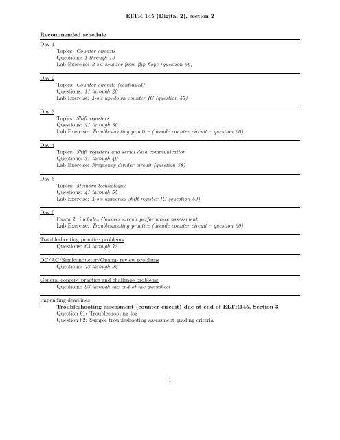
<strong>ELTR</strong> <strong>145</strong> (<strong>Digital</strong> 2), section 2<br />
Recommended schedule<br />
Day 1<br />
Day 2<br />
Day 3<br />
Day 4<br />
Day 5<br />
Day 6<br />
Topics: Counter circuits<br />
Questions: 1 through 10<br />
Lab Exercise: 2-bit counter from flip-flops (question 56)<br />
Topics: Counter circuits (continued)<br />
Questions: 11 through 20<br />
Lab Exercise: 4-bit up/down counter IC (question 57)<br />
Topics: Shift registers<br />
Questions: 21 through 30<br />
Lab Exercise: Troubleshooting practice (decade counter circuit – question 60)<br />
Topics: Shift registers and serial data communication<br />
Questions: 31 through 40<br />
Lab Exercise: Frequency divider circuit (question 58)<br />
Topics: Memory technologies<br />
Questions: 41 through 55<br />
Lab Exercise: 4-bit universal shift register IC (question 59)<br />
Exam 2: includes Counter circuit performance assessment<br />
Lab Exercise: Troubleshooting practice (decade counter circuit – question 60)<br />
Troubleshooting practice problems<br />
Questions: 63 through 72<br />
DC/AC/Semiconductor/Opamp review problems<br />
Questions: 73 through 92<br />
General concept practice and challenge problems<br />
Questions: 93 through the end of the worksheet<br />
Impending deadlines<br />
Troubleshooting assessment (counter circuit) due at end of <strong>ELTR</strong><strong>145</strong>, Section 3<br />
Question 61: Troubleshooting log<br />
Question 62: Sample troubleshooting assessment grading criteria<br />
1
<strong>ELTR</strong> <strong>145</strong> (<strong>Digital</strong> 2), section 2<br />
Skill standards addressed by this course section<br />
EIA Raising the Standard; Electronics Technician Skills for Today and Tomorrow, June 1994<br />
F Technical Skills – <strong>Digital</strong> Circuits<br />
F.14 Understand principles and operations of types of registers and counters.<br />
F.15 Fabricate and demonstrate types of registers and counters.<br />
F.16 Troubleshoot and repair types of registers and counters.<br />
B Basic and Practical Skills – Communicating on the Job<br />
B.01 Use effective written and other communication skills. Met by group discussion and completion of labwork.<br />
B.03 Employ appropriate skills for gathering and retaining information. Met by research and preparation<br />
prior to group discussion.<br />
B.04 Interpret written, graphic, and oral instructions. Met by completion of labwork.<br />
B.06 Use language appropriate to the situation. Met by group discussion and in explaining completed labwork.<br />
B.07 Participate in meetings in a positive and constructive manner. Met by group discussion.<br />
B.08 Use job-related terminology. Met by group discussion and in explaining completed labwork.<br />
B.10 Document work projects, procedures, tests, and equipment failures. Met by project construction and/or<br />
troubleshooting assessments.<br />
C Basic and Practical Skills – Solving Problems and Critical Thinking<br />
C.01 Identify the problem. Met by research and preparation prior to group discussion.<br />
C.03 Identify available solutions and their impact including evaluating credibility of information, and locating<br />
information. Met by research and preparation prior to group discussion.<br />
C.07 Organize personal workloads. Met by daily labwork, preparatory research, and project management.<br />
C.08 Participate in brainstorming sessions to generate new ideas and solve problems. Met by group discussion.<br />
D Basic and Practical Skills – Reading<br />
D.01 Read and apply various sources of technical information (e.g. manufacturer literature, codes, and<br />
regulations). Met by research and preparation prior to group discussion.<br />
E Basic and Practical Skills – Proficiency in Mathematics<br />
E.01 Determine if a solution is reasonable.<br />
E.02 Demonstrate ability to use a simple electronic calculator.<br />
E.06 Translate written and/or verbal statements into mathematical expressions.<br />
E.07 Compare, compute, and solve problems involving binary, octal, decimal, and hexadecimal numbering<br />
systems.<br />
E.12 Interpret and use tables, charts, maps, and/or graphs.<br />
E.13 Identify patterns, note trends, and/or draw conclusions from tables, charts, maps, and/or graphs.<br />
E.15 Simplify and solve algebraic expressions and formulas.<br />
E.16 Select and use formulas appropriately.<br />
2
<strong>ELTR</strong> <strong>145</strong> (<strong>Digital</strong> 2), section 2<br />
Common areas of confusion for students<br />
Common mistake: How set-up time for flip-flops influences stage-to-stage propagation.<br />
When many students first examine cascaded, synchronous flip-flop circuits (where the Q output of one<br />
enters the input of the next), they wonder why pulses don’t just ripple through the whole chain of flip-flops<br />
with one clock pulse. The reason this does not happen is that each flip-flop has a finite amount of set-up<br />
time required for the input state to be stable before it is recognized at the active edge of a new clock pulse.<br />
Even with instantaneous flip-flop output state changes, the cascaded signal still cannot reach the input of<br />
the next flip-flop before the clock pulse arrives at that next flip-flop. Therefore, the fastest a logic state can<br />
progress from one flip-flop to another in a synchronous counter circuit is one flip-flop per clock pulse.<br />
3
Question 1<br />
Questions<br />
Count from zero to fifteen, in binary, keeping the bits lined up in vertical columns like this:<br />
0000<br />
0001<br />
0010<br />
. . .<br />
Now, reading from top to bottom, notice the alternating patterns of 0’s and 1’s in each place (i.e. one’s<br />
place, two’s place, four’s place, eight’s place) of the four-bit binary numbers. Note how the least significant<br />
bit alternates more rapidly than the most significant bit. Draw a timing diagram showing the respective bits<br />
as waveforms, alternating between ”low” and ”high” states, and comment on the frequency of each of the<br />
bits.<br />
file 01373<br />
Question 2<br />
Shown here is a simple two-bit binary counter circuit:<br />
V DD<br />
LSB<br />
V DD<br />
MSB<br />
J<br />
Q<br />
J<br />
Q<br />
C<br />
C<br />
K<br />
Q<br />
K<br />
Q<br />
The Q output of the first flip-flop constitutes the least significant bit (LSB), while the second flip-flop’s<br />
Q output constitutes the most significant bit (MSB).<br />
Based on a timing diagram analysis of this circuit, determine whether it counts in an up sequence (00,<br />
01, 10, 11) or a down sequence (00, 11, 10, 01). Then, determine what would have to be altered to make it<br />
count in the other direction.<br />
file 01374<br />
4
Question 3<br />
Counter circuits built by cascading the output of one flip-flop to the clock input of the next flip-flop are<br />
generally referred to as ripple counters. Explain why this is so. What happens in such a circuit that earns<br />
it the label of ”ripple”? Is this effect potentially troublesome in circuit operation, or is it something of little<br />
or no consequence?<br />
file 01388<br />
Question 4<br />
A style of counter circuit that completely circumvents the ”ripple” effect is called the synchronous<br />
counter:<br />
V DD<br />
Q 0 Q 1<br />
J<br />
Q<br />
J<br />
Q<br />
Clock<br />
C<br />
C<br />
K<br />
Q<br />
K<br />
Q<br />
Complete a timing diagram for this circuit, and explain why this design of counter does not exhibit<br />
”ripple” on its output lines:<br />
Clock<br />
V DD<br />
Gnd<br />
V DD<br />
Q 0<br />
Gnd<br />
V DD<br />
Q 1<br />
Gnd<br />
Challenge question: to really understand this type of counter circuit well, include propagation delays in<br />
your timing diagram.<br />
file 01396<br />
5
Question 5<br />
A student just learned how a two-bit synchronous binary counter works, and he is excited about building<br />
his own. He does so, and the circuit works perfectly.<br />
V DD<br />
Q 0 Q 1<br />
J<br />
Q<br />
J<br />
Q<br />
Clock<br />
C<br />
C<br />
K<br />
Q<br />
K<br />
Q<br />
After that success, student tries to expand on their success by adding more flip-flops, following the same<br />
pattern as the two original flip-flops:<br />
V DD<br />
Q 0<br />
Q 1<br />
J Q<br />
Q 2 Q 3<br />
J<br />
Q<br />
J<br />
Q<br />
J<br />
Q<br />
Clock<br />
C<br />
C<br />
C<br />
C<br />
K<br />
Q<br />
K<br />
Q<br />
K<br />
Q<br />
K<br />
Q<br />
Unfortunately, this circuit didn’t work. The sequence it generates is not a binary count. Determine<br />
what the counting sequence of this circuit is, and then try to figure out what modifications would be required<br />
to make it count in a proper binary sequence.<br />
file 01397<br />
6
Question 6<br />
Complete a timing diagram for this synchronous counter circuit, and identify the direction of its binary<br />
count:<br />
V DD<br />
Q 0 Q 1<br />
J<br />
Q<br />
J<br />
Q<br />
Clock<br />
C<br />
C<br />
K<br />
Q<br />
K<br />
Q<br />
Clock<br />
V DD<br />
Gnd<br />
V DD<br />
Q 0<br />
Gnd<br />
V DD<br />
Q 1<br />
Gnd<br />
file 01398<br />
7
Question 7<br />
Synchronous counter circuits tend to confuse students. The circuit shown here is the design that most<br />
students think ought to work, but actually doesn’t:<br />
V DD<br />
Q 2 Q 3<br />
J<br />
Q<br />
J<br />
Q 0 Q 1<br />
J Q<br />
Q<br />
J<br />
Q<br />
Clock<br />
C<br />
C<br />
C<br />
C<br />
K<br />
Q<br />
K<br />
Q<br />
K<br />
Q<br />
K<br />
Q<br />
Shown here is an up/down synchronous counter design that does work:<br />
Up/Down<br />
V DD<br />
Q 0 Q 1 Q 2 Q 3<br />
J<br />
Q<br />
J<br />
Q<br />
J<br />
Q<br />
J<br />
Q<br />
Clock<br />
C<br />
C<br />
C<br />
C<br />
K<br />
Q<br />
K<br />
Q<br />
K<br />
Q<br />
K<br />
Q<br />
Explain why this circuit is able to function properly (counting in either direction), while the first circuit<br />
is not able to count properly at all. What do those ”extra” gates do to make the counter circuit function<br />
as it should. Hint: to more easily compare the up/down counter to the faulty up counter initially shown,<br />
connect the Up/Down control line high, and then disregard any lines and gates that become disabled as a<br />
result.<br />
file 01400<br />
8
Question 8<br />
The following circuit is a two-bit synchronous binary up/down counter:<br />
Up/Down<br />
V DD<br />
Q 0 Q 1<br />
J<br />
Q<br />
J<br />
Q<br />
Clock<br />
C<br />
C<br />
K<br />
Q<br />
K<br />
Q<br />
Explain what would happen if the upper AND gate’s output were to become ”stuck” in the high state<br />
regardless of its input conditions. What effect would this kind of failure have on the counter’s operation?<br />
file 01399<br />
Question 9<br />
Supposed we used J-K flip-flops with asynchronous inputs (Preset and Clear) to build a counter:<br />
PRE<br />
Up/Down<br />
V DD<br />
Q 0 Q 1 Q 2 Q 3<br />
J<br />
PRE Q<br />
J PRE Q<br />
J PRE Q<br />
J PRE<br />
Q<br />
Clock<br />
C<br />
C<br />
C<br />
C<br />
K<br />
Q<br />
K Q<br />
K Q<br />
K<br />
CLR CLR CLR CLR<br />
Q<br />
CLR<br />
With the asynchronous lines paralleled as such, what are we able to make the counter do now that we<br />
weren’t before we had asynchronous inputs available to us?<br />
file 01401<br />
9
Question 10<br />
The part number 74HCT163 integrated circuit is a high-speed CMOS, four-bit, synchronous binary<br />
counter. It is a pre-packaged unit, will all the necessary flip-flops and selection logic enclosed to make your<br />
design work easier than if you had to build a counter circuit from individual flip-flops. Its block diagram<br />
looks something like this (power supply terminals omitted, for simplicity):<br />
SPE<br />
PE<br />
P 0<br />
P 1 P 2 P 3<br />
TE<br />
CP<br />
74HCT163<br />
TC<br />
Q 0 Q 1 Q 2 Q 3<br />
MR<br />
Research the function of this integrated circuit, from manufacturers’ datasheets, and explain the function<br />
of each input and output terminal.<br />
file 01403<br />
10
Question 11<br />
Determine the output pulses for this counter circuit, known as a Johnson counter, assuming that all Q<br />
outputs begin in the low state:<br />
D<br />
Q<br />
0<br />
D<br />
Q<br />
1<br />
D<br />
Q<br />
D<br />
Q<br />
2 3<br />
Clk<br />
C<br />
C<br />
C<br />
C<br />
Q<br />
Q<br />
Q<br />
Q<br />
Clock<br />
V DD<br />
Gnd<br />
V DD<br />
Q 0<br />
Gnd<br />
V DD<br />
Q 1<br />
Gnd<br />
V DD<br />
Q 2<br />
Gnd<br />
V DD<br />
Q 3<br />
Gnd<br />
file 01427<br />
11
Question 12<br />
The following circuit is known as a Johnson counter:<br />
D<br />
Q<br />
D<br />
Q<br />
D<br />
Q<br />
D<br />
Q<br />
C<br />
C<br />
C<br />
C<br />
Q<br />
Q<br />
Q<br />
Q<br />
Clock<br />
Describe the output of this circuit, as measured from the Q output of the far right flip-flop, assuming<br />
that all flip-flops power up in the reset condition.<br />
Also, explain what this modified version of the above Johnson counter circuit will do, in each of the five<br />
selector switch positions:<br />
D<br />
Q<br />
D<br />
Q<br />
D<br />
Q<br />
D<br />
Q<br />
C<br />
C<br />
C<br />
C<br />
Q<br />
Q<br />
Q<br />
Q<br />
Clock<br />
2<br />
3<br />
4<br />
5<br />
1<br />
Output<br />
file 01475<br />
12
Question 13<br />
Suppose we had two four-bit synchronous up/down counter circuits, which we wished to cascade to<br />
make one eight-bit counter. Draw the necessary connecting wires (and any extra gates) between the two<br />
four-bit counters to make this possible:<br />
Up/Down<br />
V DD<br />
Q 0 Q 1 Q 2 Q 3<br />
J<br />
Q<br />
J<br />
Q<br />
J<br />
Q<br />
J<br />
Q<br />
Clock<br />
C<br />
K<br />
Q<br />
C<br />
K<br />
Q<br />
C<br />
K<br />
Q<br />
C<br />
K<br />
Q<br />
Up/Down<br />
Q 4 Q 5 Q 6 Q 7<br />
J<br />
Q<br />
J<br />
Q<br />
J<br />
Q<br />
J<br />
Q<br />
Clock<br />
C<br />
K<br />
Q<br />
C<br />
K<br />
Q<br />
C<br />
K<br />
Q<br />
C<br />
K<br />
Q<br />
After deciding how to cascade these counters, imagine that you are in charge of building and packaging<br />
four-bit counter circuits. The customers who buy your counters might wish to cascade them as you did<br />
here, but they won’t have the ability to ”go inside” the packaging as you did to connect to any of the lines<br />
between the various flip-flops. This means you will have to provide any necessary cascading lines as inputs<br />
and outputs on your pre-packaged counters. Think carefully about how you would choose to build and<br />
package your four-bit ”cascadable” counters, and then draw a schematic diagram.<br />
file 01402<br />
13
Question 14<br />
Here is an eight-bit counter comprised of two four-bit 74HCT163 synchronous binary counters cascaded<br />
together:<br />
V DD<br />
V DD<br />
SPE<br />
SPE<br />
V DD<br />
P 0<br />
P 1 P 2 P 3<br />
V DD<br />
P 0<br />
P 1 P 2 P 3<br />
PE<br />
TE<br />
74HCT163<br />
TC<br />
GND<br />
PE<br />
TE<br />
74HCT163<br />
TC<br />
GND<br />
MR<br />
CP<br />
Q 0 Q 1 Q 2 Q 3<br />
MR<br />
CP<br />
Q 0 Q 1 Q 2 Q 3<br />
Four output bits<br />
Four output bits<br />
Explain how this counter circuit works, and also determine which output bit is the LSB and which is<br />
the MSB.<br />
Now, examine this eight-bit counter comprised of the same two ICs:<br />
V DD<br />
V DD<br />
SPE<br />
SPE<br />
V DD<br />
P 0<br />
P 1 P 2 P 3<br />
V DD<br />
P 0<br />
P 1 P 2 P 3<br />
PE<br />
TE<br />
74HCT163<br />
TC<br />
GND<br />
PE<br />
TE<br />
74HCT163<br />
TC<br />
GND<br />
MR<br />
CP<br />
Q 0 Q 1 Q 2 Q 3<br />
MR<br />
CP<br />
Q 0 Q 1 Q 2 Q 3<br />
Four output bits<br />
Four output bits<br />
Explain how this counter circuit works, and how its operation differs from the previous eight-bit counter<br />
circuit.<br />
file 02952<br />
14
Question 15<br />
A student wishes to cascade multiple four-bit synchronous counters together. His first effort looks like<br />
this, and it works well as an eight-bit counter:<br />
V DD<br />
V DD<br />
RST<br />
EN<br />
V DD<br />
TC<br />
CLK<br />
CTR<br />
GND<br />
Q 0 Q 1 Q 2 Q 3<br />
RST<br />
EN<br />
V DD<br />
TC<br />
CLK<br />
CTR<br />
GND<br />
Q 0 Q 1 Q 2 Q 3<br />
Four output bits<br />
Four output bits<br />
Encouraged by this success, the student decides to add another four-bit counter to the end to make a<br />
twelve-bit counter circuit:<br />
V DD<br />
RST<br />
EN<br />
V DD<br />
TC<br />
CLK<br />
CTR<br />
GND<br />
Q 0 Q 1 Q 2 Q 3<br />
RST<br />
EN<br />
V DD<br />
Q 0 Q 1 Q 2 Q 3<br />
TC<br />
V DD<br />
V DD<br />
TC<br />
CLK<br />
CTR<br />
GND<br />
Q 0 Q 1 Q 2 Q 3<br />
RST<br />
EN<br />
CLK<br />
V DD<br />
CTR<br />
GND<br />
Four output bits<br />
Four output bits<br />
Four output bits<br />
Unfortunately, this arrangement does not work so well. It seems to work good for the first 241 counts<br />
(from 000000000000 to 000011110000), but then the last four bits begin to cycle as quickly as the first four<br />
bits, while the middle four bits remain in the 1111 state for 15 additional clock pulses. Something is definitely<br />
very wrong here!<br />
Determine what the problem is, and suggest a remedy for it. Hint: this situation is very similar to<br />
connecting more than two J-K flip-flops together to form a synchronous counter circuit.<br />
file 02954<br />
15
Question 16<br />
Some integrated circuit counters come equipped with multiple enable inputs. A good example of this is<br />
the 74HCT163:<br />
SPE<br />
Enable inputs<br />
PE<br />
TE<br />
CP<br />
P 0<br />
P 1 P 2 P 3<br />
74HCT163 TC<br />
Q 0 Q 1 Q 2 Q 3<br />
MR<br />
In this case, as in others, the two enable inputs are not identical. Although both must be active for the<br />
counter to count, one of the enable inputs does something extra that the other one does not. This additional<br />
function is often referred to as a look-ahead carry, provided to simplify cascading of counters.<br />
Explain what ”look-ahead carry” means in the context of digital counter circuits, and why it is a useful<br />
feature.<br />
file 02955<br />
Question 17<br />
Determine the modulus (MOD) of a four-bit binary counter. Determine the modulus of two four-bit<br />
binary counters cascaded to make an eight-bit binary counter.<br />
file 01404<br />
16
Question 18<br />
Consider the following four-bit binary counter integrated circuit (IC). When clocked by the square wave<br />
signal generator, it counts from 0000 to 1111 in sixteen steps and then ”recycles” back to 0000 again in a<br />
single step:<br />
V DD<br />
RST<br />
EN<br />
V DD<br />
TC<br />
CLK CTR<br />
GND<br />
Q 0 Q 1 Q 2 Q 3<br />
There are many applications, though, where we do not wish the counter circuit to count all the way up<br />
to full count (1111), but rather recycle at some lesser terminal count value. Take for instance the application<br />
of BCD counting: from 0000 to 1001 and back again. Here is one way to truncate the counting sequence of<br />
a binary counter so that it becomes a BCD counter:<br />
V DD<br />
RST<br />
EN<br />
V DD<br />
TC<br />
CLK CTR<br />
GND<br />
Q 0 Q 1 Q 2 Q 3<br />
Explain how the NAND gate forces this counter to recycle after an output of 1001 instead of counting<br />
all the way up to 1111. (Hint: the reset function of this IC is assumed to be asynchronous, meaning the<br />
counter output resets to 0000 immediately when the RST terminal goes low.)<br />
Also, show how you would modify this circuit to do the same count sequence (BCD) assuming the IC<br />
has a synchronous reset function, meaning the counter resets to 0000 if RST is low and the clock input sees<br />
a pulse.<br />
file 02953<br />
17
Question 19<br />
Suppose you had an astable multivibrator circuit that output a very precise 1 Hz square-wave signal, but<br />
you had an application which requires a pulse once every minute rather than once every second. Knowing<br />
that there are 60 seconds in a minute, can you think of a way to use digital counters to act as a ”frequency<br />
divider” so that every 60 multivibrator pulses equates to 1 output pulse?<br />
You don’t have a divide-by-60 counter available, but you do have several divide-by-10 (”decade”)<br />
counters at your disposal. Engineer a solution using these counter units:<br />
EN P<br />
Decade CTR<br />
EN P<br />
Decade CTR<br />
EN T<br />
RCO<br />
EN T<br />
RCO<br />
CLK<br />
CLK<br />
Q A Q B Q C Q D<br />
Q A Q B Q C Q D<br />
CLR<br />
CLR<br />
Note: assume these counter ICs have asynchronous resets.<br />
file 01405<br />
Question 20<br />
When counters are used as frequency dividers, they are often drawn as simple boxes with one input and<br />
one output each, like this:<br />
MOD-10 MOD-6 MOD-2 MOD-5<br />
f in<br />
f out1 f out2 f out3 f out4<br />
Calculate the four output frequencies (f out1 through f out4 ) given an input frequency of 1.5 kHz:<br />
• f out1 =<br />
• f out2 =<br />
• f out3 =<br />
• f out4 =<br />
file 02956<br />
18
Question 21<br />
Complete the timing diagram for this circuit, assuming all Q outputs begin in the low state:<br />
V DD Q 0 Q 1 Q 2 Q 3<br />
D<br />
Q<br />
D<br />
Q<br />
D<br />
Q<br />
D<br />
Q<br />
C<br />
C<br />
C<br />
C<br />
Q<br />
Q<br />
Q<br />
Q<br />
Clock<br />
Clock<br />
V DD<br />
Gnd<br />
V DD<br />
Q 0<br />
Gnd<br />
V DD<br />
Q 1<br />
Gnd<br />
V DD<br />
Q 2<br />
Gnd<br />
V DD<br />
Q 3<br />
Gnd<br />
file 02986<br />
19
Question 22<br />
Complete the timing diagram for this circuit, assuming all Q outputs begin in the low state:<br />
Q 0 Q 1 Q 2 Q 3<br />
D<br />
Q<br />
D<br />
Q<br />
D<br />
Q<br />
D<br />
Q<br />
C<br />
C<br />
C<br />
C<br />
Q<br />
Q<br />
Q<br />
Q<br />
Clock<br />
Clock<br />
V DD<br />
Gnd<br />
V DD<br />
Q 0<br />
Gnd<br />
V DD<br />
Q 1<br />
Gnd<br />
V DD<br />
Q 2<br />
Gnd<br />
V DD<br />
Q 3<br />
Gnd<br />
file 02987<br />
Question 23<br />
What is the definition of a register in the context of digital circuitry? Also, define and compare/contrast<br />
what a shift register is.<br />
file 02989<br />
Question 24<br />
Explain the difference between serial digital data and parallel digital data.<br />
file 01466<br />
20
Question 25<br />
A helpful analogy for a shift register is a conveyor belt. Examine this illustration showing a single<br />
conveyor belt at four different times, and determine which of the following shift register operations the<br />
sequence represents:<br />
• Parallel-in, serial-out<br />
• Parallel-in, parallel-out<br />
• Serial-in, serial-out<br />
• Serial-in, parallel-out<br />
Step 1 Step 2 Step 3 Step 4<br />
file 02961<br />
Question 26<br />
A helpful analogy for a shift register is a conveyor belt. Examine this illustration showing a single<br />
conveyor belt at four different times, and determine which of the following shift register operations the<br />
sequence represents:<br />
• Parallel-in, serial-out<br />
• Parallel-in, parallel-out<br />
• Serial-in, serial-out<br />
• Serial-in, parallel-out<br />
Step 1 Step 2 Step 3 Step 4<br />
file 02985<br />
21
Question 27<br />
A helpful analogy for a shift register is a conveyor belt. Examine this illustration showing a single<br />
conveyor belt at four different times, and determine which of the following shift register operations the<br />
sequence represents:<br />
• Parallel-in, serial-out<br />
• Parallel-in, parallel-out<br />
• Serial-in, serial-out<br />
• Serial-in, parallel-out<br />
Step 1 Step 2 Step 3 Step 4<br />
file 02960<br />
Question 28<br />
Draw the necessary connecting wires between flip-flops so that serial data is shifted from right to left<br />
instead of left to right as you may be accustomed to seeing in a shift register schematic:<br />
D<br />
Q<br />
D<br />
Q<br />
D<br />
Q<br />
D<br />
Q<br />
D<br />
Q<br />
D<br />
Q<br />
D<br />
Q<br />
D<br />
Q<br />
C<br />
C<br />
C<br />
C<br />
C<br />
C<br />
C<br />
C<br />
Q<br />
Q<br />
Q<br />
Q<br />
Q<br />
Q<br />
Q<br />
Q<br />
Clock<br />
Be sure to also note where data enters this shift register, and where data exits.<br />
file 01471<br />
Question 29<br />
Explain how a shift register circuit could be built from D-type flip-flops with the ability to shift data<br />
either to the right or to the left, on command. I’m not necessarily asking for a schematic diagram so much as<br />
I’m looking for an explanation of how such a circuit might be built. Of course, if your best way of presenting<br />
your idea is to draw a schematic diagram, go ahead!<br />
file 01472<br />
22
Question 30<br />
Explain what a universal shift register is. The 74194 is an example of a TTL universal shift register, so<br />
you will find that datasheet very helpful in answering this question.<br />
file 01470<br />
23
Question 31<br />
Switch contact bounce is often a problem when connecting mechanical contact switches or relays to the<br />
inputs of digital semiconductor circuits. When a switch transitions from open to closed, or from closed to<br />
open, there is usually a burst of on/off pulses rather than a single, crisp, change of logic state:<br />
V DD<br />
R pulldown<br />
V out<br />
Switch actuated:<br />
Closed<br />
Open<br />
"Bounce"<br />
Switch de-actuated:<br />
Closed<br />
Open<br />
<strong>Digital</strong> electronic circuits, of course, react to these pulses as though they were very rapid actuations/deactuations<br />
of the switch. This may cause problems, especially in applications where a mechanical switch<br />
input causes a counter to increment or decrement!<br />
To fix this problem we must properly condition the switch signal to eliminate the spurious on/off pulses.<br />
The process of doing this is called debouncing. There is more than one way to de-bounce a switch, but one<br />
of the more sophisticated ways uses a serial-in, serial-out shift register with an asynchronous reset (clear)<br />
input:<br />
24
V DD<br />
"Debounced" output<br />
D<br />
Q<br />
D<br />
Q<br />
D<br />
Q<br />
D<br />
Q<br />
C<br />
C<br />
C<br />
C<br />
Clock<br />
Q<br />
Q<br />
Q<br />
Q<br />
RST<br />
RST RST RST<br />
V DD<br />
R pulldown<br />
Explain how this circuit works to de-bounce the switch’s ”dirty” signal, producing a ”clean” (debounced)<br />
signal for a subsequent digital circuit’s input.<br />
file 02990<br />
25
Question 32<br />
An analog-to-digital converter is a circuit that inputs an analog signal and outputs a multiple-bit binary<br />
number equivalent to that signal’s amplitude:<br />
+V<br />
ADC<br />
D 0<br />
V in<br />
V ref<br />
In<br />
12-bit output<br />
Ref in<br />
D 11<br />
A free-running analog-to-digital converter is one that updates its digital output as often as it can, not<br />
waiting for any prompting from another device. If we were to connect a free-running ADC to a computer<br />
(microprocessor or microcontroller), we would need some way to sample the ADC’s output at times specified<br />
by the computer, and hold that binary number long enough for the computer to register it. Otherwise, the<br />
ADC may update its output in the middle of one of the computer’s ”input” cycles, possibly resulting in<br />
corrupted data.<br />
We could build such a sample-and-hold circuit out of flip-flops. What type of flip-flop would we use for<br />
this purpose, and how many would we need for the ADC circuit shown above? This circuit we would build<br />
is also known as a shift register. What kind of shift register inputs multiple bits of data all at once, and<br />
transfers that data to its output lines all at once, at the command of a clock pulse?<br />
file 01465<br />
Question 33<br />
An important function in computer circuitry is serial-to-parallel data conversion, where a stream of<br />
serial data is ”read” one bit at a time, then all bits output at once in parallel form. A shift register circuit<br />
is ideal for this application. Shown here is an eight-bit shift register circuit:<br />
D<br />
Q<br />
D<br />
Q<br />
D<br />
Q<br />
D<br />
Q<br />
D<br />
Q<br />
D<br />
Q<br />
D<br />
Q<br />
D<br />
Q<br />
C<br />
C<br />
C<br />
C<br />
C<br />
C<br />
C<br />
C<br />
Q<br />
Q<br />
Q<br />
Q<br />
Q<br />
Q<br />
Q<br />
Q<br />
Clock<br />
Draw any necessary wires and labels showing where serial data would enter the circuit, and where<br />
parallel data would exit.<br />
file 01468<br />
26
Question 34<br />
The following schematic diagram is for a two-input selector circuit, which (as the name implies) selects<br />
one of two inputs to be sent to the output:<br />
Input A<br />
Select<br />
control<br />
Output<br />
Input B<br />
Determine what state the ”select control” input line has to be in to select Input A to be sent to the<br />
output, and what state it has to be in to select Input B to go to the output.<br />
file 03065<br />
Question 35<br />
Suppose we wished to use a shift register circuit to input several binary bits at once (parallel data<br />
transfer), and then output the bits one at a time over a single line (serial data transfer). You should be<br />
aware of how shift registers are constructed with D-type flip-flops. Now, describe how we can get parallel<br />
data entered into a shift register circuit. Note: there is more than one answer to this question!<br />
file 01469<br />
Question 36<br />
The following schematic diagram shows two four-bit universal shift registers used to communicate data<br />
serially over a coaxial cable of unspecified length:<br />
Parallel data in<br />
PL<br />
CE<br />
Clk<br />
D S<br />
V SS<br />
D 0 D 1 D 2 D 3<br />
SRG<br />
Q 0 Q 1 Q 2 Q 3<br />
Coaxial data cable<br />
. . .<br />
PL<br />
CE<br />
Clk<br />
D S<br />
V SS<br />
D 0 D 1 D 2 D 3<br />
SRG<br />
Q 0 Q 1 Q 2 Q 3<br />
Parallel data out<br />
Specify what logic states would have to be input at the PL, CE, and Clk terminals of each shift register,<br />
and at what times, to successfully load four bits of parallel data, shift them serially over the coaxial data<br />
cable, and then hold them at the outputs (Q) of the receiving shift register.<br />
file 02997<br />
27
Question 37<br />
Personal computers and peripheral devices provide a rich source of examples for both serial and parallel<br />
data transmission. Identify some common examples of both serial and parallel data transmission networks<br />
(and standards) at work in a common personal computer. Examples may include communication between<br />
computers, between computers and peripheral devices (printers, scanners, cameras, special cards), or between<br />
fundamental components of the computer (CPU, disk drive, monitor, etc.).<br />
file 02993<br />
Question 38<br />
A ubiquitous example of serial data communication is the cable linking a keyboard to a personal<br />
computer: for every key switch pressed, an ASCII character is transmitted to the computer. An interesting<br />
characteristic of this particular communication protocol is the random rate at which the ASCII characters<br />
are sent. Because the characters are generated at the rate the computer user happens to type, the rate is<br />
completely unpredictable. Consequently, this form of serial data communication is known as asynchronous.<br />
Compare and contrast this against synchronous serial data communication, giving an example of a<br />
synchronous data communications standard.<br />
file 02995<br />
Question 39<br />
An important integrated circuit (IC) used in digital data communication is a UART. Describe what this<br />
acronym stands for, and explain the purpose of this circuit.<br />
file 02994<br />
28
Question 40<br />
Shown here are three different telegraph circuits. Determine which of these could be classified as simplex,<br />
full-duplex, and half-duplex, in terms of serial data transmission:<br />
. . .<br />
. . .<br />
. . .<br />
. . .<br />
. . .<br />
. . .<br />
file 01284<br />
Question 41<br />
. . .<br />
When <strong>Digital</strong> Audio Tape (DAT) was first introduced to the American public, it was touted as delivering<br />
superior sound quality. Most importantly, this high quality of sound was not supposed to degrade over time<br />
like standard (analog) audio cassette tape recordings.<br />
The magnetic media from which DAT was manufactured was basically the same stuff used to make<br />
analog audio tape. Explain why the encoding of audio data digitally on the same media would provide<br />
superior resistance to degradation over analog recordings even though the recording media was the same.<br />
Also, explain how this is significant to modern digital data storage technologies such as those used to store<br />
photographic images and numerical data.<br />
file 01441<br />
29
Question 42<br />
Define the following terms, as they relate to digital memory devices:<br />
• RAM:<br />
• ROM:<br />
• Volatile:<br />
• Nonvolatile:<br />
In particular, explain why ”RAM” is a misleading term.<br />
file 01439<br />
Question 43<br />
Determine whether the following recording devices are random access or sequential access, and discuss<br />
the advantage(s) of one type of access over the other:<br />
• DVD (disk)<br />
• Audio tape cassette<br />
• CD-ROM (disk)<br />
• ROM memory chip<br />
• Vinyl phonograph record<br />
• Video tape cassette<br />
• Magnetic ”hard” drive<br />
• Magnetic bubble memory<br />
• Paper tape (a long strip of tape with holes punched in it)<br />
• RAM memory chip<br />
file 01440<br />
Question 44<br />
Define the following acronyms:<br />
• ROM:<br />
• PROM:<br />
• EPROM:<br />
• EEPROM:<br />
• UVEPROM:<br />
Be prepared to explain a few things about each of these memory technologies: how they work, what<br />
applications they might be found in, advantages and disadvantages of each.<br />
file 01449<br />
Question 45<br />
Explain the difference between static RAM (”SRAM”) and dynamic RAM (”DRAM”) memory<br />
technologies. Which type of memory technology provides faster access of data, and why? Which type<br />
of memory technology provides the greatest storage density, and why?<br />
file 01442<br />
Question 46<br />
Flash memory is a nonvolatile memory technology, offering greater density than either SRAM or DRAM,<br />
and faster erasure than standard EPROMs. At first, it would seem Flash memory outperforms all other<br />
memory types, but it doesn’t. What are some of the disadvantages of Flash memory, and what kind of<br />
applications is it best suited for?<br />
file 0<strong>145</strong>2<br />
30
Question 47<br />
Two very important concepts to understand when working with digital memory devices are address and<br />
data. Define each of these terms in your own words.<br />
file 01444<br />
Question 48<br />
A ROM memory chip is rated at 4k × 8 bits. What, exactly, does this designation mean? How many<br />
addresses are there inside this memory chip? How many bits of storage are there, total, in this memory<br />
chip? How many address bits are there, and how many data bits are there?<br />
file 01443<br />
Question 49<br />
Suppose you need to store a text message in digital memory, consisting of 7500 ASCII characters. What<br />
is the most logical memory <strong>org</strong>anization (addresses × data lines) to do this? How many address bits would<br />
be needed to store these 7500 characters?<br />
file 01445<br />
Question 50<br />
Suppose you need a memory array with 1k × 8 <strong>org</strong>anization, but all you have on hand are 1k × 4<br />
memory chips. Show how you could connect two of them to form the desired array:<br />
1k × 4 RAM<br />
A 0<br />
A 1<br />
A 2<br />
A 3<br />
D 0<br />
A 4<br />
D 1<br />
A 5<br />
D 2<br />
A 6<br />
D 3<br />
A 7<br />
A 8<br />
A 9<br />
CS<br />
R/W<br />
1k × 4 RAM<br />
A 0<br />
A 1<br />
A 2<br />
A 3<br />
D 0<br />
A 4<br />
D 1<br />
A 5<br />
D 2<br />
A 6<br />
D 3<br />
A 7<br />
A 8<br />
A 9<br />
CS<br />
R/W<br />
file 01446<br />
31
Question 51<br />
Suppose you need a memory array with 2k × 4 <strong>org</strong>anization, but all you have on hand are 1k × 4<br />
memory chips. Show how you could connect two of them to form the desired array:<br />
1k × 4 RAM<br />
A 0<br />
A 1<br />
A 2<br />
A 3<br />
D 0<br />
A 4<br />
D 1<br />
A 5<br />
D 2<br />
A 6<br />
D 3<br />
A 7<br />
A 8<br />
A 9<br />
CS<br />
R/W<br />
1k × 4 RAM<br />
A 0<br />
A 1<br />
A 2<br />
A 3<br />
D 0<br />
A 4<br />
D 1<br />
A 5<br />
D 2<br />
A 6<br />
D 3<br />
A 7<br />
A 8<br />
A 9<br />
CS<br />
R/W<br />
file 01447<br />
Question 52<br />
Dynamic RAM chips often contain more addresses than they have address lines to select them with.<br />
For example, the MCM516100 DRAM chip has an <strong>org</strong>anization of 16M × 1, yet it only has twelve address<br />
lines.<br />
Explain how it is possible to select one out of 16 million unique addresses while using only twelve address<br />
lines. Hint: the technique is known as address multiplexing. Be sure to refer to one or more dynamic RAM<br />
datasheets when doing your research!<br />
file 0<strong>145</strong>1<br />
Question 53<br />
After a ROM memory has been programmed with data, it is good to verify that the data now stored<br />
is okay, and not corrupted with any errors. A popular method of doing this is to calculate a checksum on<br />
the stored data, and compare that against the checksum for the original data. If the checksum numbers are<br />
identical, chances are there are no corruptions in the stored data.<br />
Explain exactly what checksum is, and how it works as an error-detection strategy.<br />
file 0<strong>145</strong>0<br />
32
Question 54<br />
An important use for read-only semiconductor memories is as look-up tables. Describe what a ”look-up<br />
table” is, and what one might be used for.<br />
file 01477<br />
Question 55<br />
Research datasheets for the 74LS184 and 74LS185 integrated circuits, and then explain how read-only<br />
memory technology is used to perform the BCD/binary conversion functions.<br />
file 02991<br />
33
Question 56<br />
Competency: 2-bit flip-flop counter circuit<br />
Description<br />
Version:<br />
Schematic<br />
Build a 2-bit counter circuit using individual J-K flip-flops.<br />
R limit<br />
R limit<br />
Count sequence<br />
Output timing diagram as shown by oscilloscope<br />
Predicted<br />
Actual<br />
Time<br />
Identify the counting states on the oscilloscope display (00, 01, 10, and 11).<br />
file 02947<br />
34
Question 57<br />
Competency: 4-bit up/down counter IC<br />
Description<br />
Version:<br />
Configure a 4-bit counter IC to count either up or down<br />
depending on the position of a selector switch. Complete<br />
the schematic diagram to show the switch and all other<br />
necessary components/connections.<br />
Schematic<br />
CTR<br />
V clock<br />
Q 3<br />
Q 2<br />
Q 1<br />
Q 0<br />
R limit R limit R limit R limit<br />
Count sequence<br />
Counts in the "up" direction<br />
Counts in the "down" direction<br />
file 02957<br />
35
Question 58<br />
Competency: Binary counter as frequency divider<br />
Schematic<br />
Version:<br />
CTR<br />
f clock<br />
Q 3<br />
Q 2<br />
Q 1<br />
Q 0<br />
Given conditions<br />
f clock =<br />
Parameters<br />
Predicted<br />
Measured<br />
f Q0<br />
f Q1<br />
f Q2<br />
f Q3<br />
file 02959<br />
36
Question 59<br />
Competency: 4-bit universal shift register IC<br />
Description<br />
Version:<br />
Configure a 4-bit universal shift register IC to load<br />
parallel data, then shift in both directions. Complete the<br />
schematic diagram to show all switches and other<br />
necessary components/connections.<br />
Schematic<br />
D 3<br />
D 2<br />
SRG<br />
D 1<br />
D 0<br />
Q 3<br />
Q 2<br />
Q 1<br />
Q 0<br />
V clock<br />
R limit R limit R limit R limit<br />
Shift sequence<br />
Loads parallel data<br />
Shifts right<br />
Shifts left<br />
file 02958<br />
37
Question 60<br />
Competency: Decade counter circuit<br />
Schematic<br />
Version:<br />
Reset<br />
Event switch<br />
Counter IC<br />
U 1 U<br />
A 2<br />
RST<br />
B<br />
CTR<br />
C<br />
Clk<br />
D<br />
Seven-segment display<br />
Display driver IC<br />
a<br />
a<br />
b<br />
c d<br />
e fg<br />
e<br />
f<br />
d<br />
g<br />
c<br />
b<br />
Details purposely omitted from schematic diagram<br />
Given conditions<br />
U 1 = U 2 =<br />
Parameters<br />
Counter increments with each physical event,<br />
counting from 0 to 9 and then resetting back<br />
to 0 again. Count sequence exhibits no skipped<br />
counts and no missed events.<br />
YES<br />
NO<br />
file 03851<br />
38
Question 61<br />
Actions / Measurements / Observations<br />
(i.e. What I did and/or noticed . . . )<br />
Troubleshooting log<br />
Conclusions<br />
(i.e. What this tells me . . . )<br />
file 03933<br />
39
Question 62<br />
NAME:<br />
Troubleshooting Grading Criteria<br />
You will receive the highest score for which all criteria are met.<br />
100 % (Must meet or exceed all criteria listed)<br />
A. Absolutely flawless procedure<br />
B. No unnecessary actions or measurements taken<br />
90 % (Must meet or exceed these criteria in addition to all criteria for 85% and below)<br />
A. No reversals in procedure (i.e. changing mind without sufficient evidence)<br />
B. Every single action, measurement, and relevant observation properly documented<br />
80 % (Must meet or exceed these criteria in addition to all criteria for 75% and below)<br />
A. No more than one unnecessary action or measurement<br />
B. No false conclusions or conceptual errors<br />
C. No missing conclusions (i.e. at least one documented conclusion for action / measurement / observation)<br />
70 % (Must meet or exceed these criteria in addition to all criteria for 65%)<br />
A. No more than one false conclusion or conceptual error<br />
B. No more than one conclusion missing (i.e. an action, measurement, or relevant observation without a<br />
corresponding conclusion)<br />
65 % (Must meet or exceed these criteria in addition to all criteria for 60%)<br />
A. No more than two false conclusions or conceptual errors<br />
B. No more than two unnecessary actions or measurements<br />
C. No more than one undocumented action, measurement, or relevant observation<br />
D. Proper use of all test equipment<br />
60 % (Must meet or exceed these criteria)<br />
A. Fault accurately identified<br />
B. Safe procedures used at all times<br />
50 % (Only applicable where students performed significant development/design work – i.e. not a proven<br />
circuit provided with all component values)<br />
A. Working prototype circuit built and demonstrated<br />
0 % (If any of the following conditions are true)<br />
A. Unsafe procedure(s) used at any point<br />
file 03932<br />
Question 63<br />
A student builds a four-bit asynchronous counter circuit using CMOS J-K flip-flops. It seems to work .<br />
. . most of the time. Every once in a while, the count suddenly and mysteriously ”jumps” out of sequence,<br />
to a value that is completely wrong. Even stranger than this is the fact that it seems to happen every time<br />
the student waves their hand next to the circuit.<br />
What do you suspect the problem to be?<br />
file 01406<br />
40
Question 64<br />
Identify a single fault that would allow this synchronous counter circuit to count up on demand, but<br />
not down:<br />
Up/Down<br />
Clock<br />
V DD<br />
J<br />
C<br />
K<br />
U U<br />
U U 7 U 10 U 13 5<br />
Q 0 Q 1 Q 2 Q 3<br />
U 6<br />
Q<br />
U 8 K Q<br />
U 11 K Q<br />
U 14 K Q<br />
Q<br />
J Q<br />
9<br />
J Q<br />
12<br />
J Q<br />
U 1 U 2 U 3 U 4<br />
C<br />
C<br />
C<br />
Explain why your proposed fault would cause the problem.<br />
file 03897<br />
Question 65<br />
A student builds a four-bit asynchronous up counter out of individual J-K flip-flops, but is dissatisfied<br />
with its performance:<br />
V DD<br />
V DD<br />
S<br />
V DD V DD V DD V DD V DD V DD<br />
Q 0 Q 1 Q 2 Q 3<br />
S<br />
S<br />
S<br />
J<br />
J<br />
J<br />
Q<br />
J<br />
Q<br />
Q<br />
Q<br />
C<br />
C<br />
C<br />
C<br />
K<br />
Q<br />
K<br />
Q<br />
K<br />
Q<br />
K<br />
Q<br />
V DD<br />
R<br />
V DD<br />
R<br />
V DD<br />
R<br />
V DD<br />
R<br />
Although the counting sequence is proper, the circuit usually does not begin counting from 0000 at<br />
power-up. The fact that the circuit counts correctly suggests that there is nothing failed or mis-wired, so<br />
what could possibly be wrong?<br />
file 03901<br />
41
Question 66<br />
The following RC circuit constitutes an automatic reset network for the counter. At power-up, it resets<br />
the counter to 0000, then allows it to count normally:<br />
V DD<br />
V DD<br />
R 1<br />
C 1<br />
R 2<br />
R 3<br />
−<br />
+<br />
RST<br />
EN<br />
V DD<br />
TC<br />
CLK CTR<br />
GND<br />
Q 0 Q 1 Q 2 Q 3<br />
Predict how the operation of this automatic reset circuit will be affected as a result of the following<br />
faults. Consider each fault independently (i.e. one at a time, no multiple faults):<br />
• Resistor R 1 fails open:<br />
• Resistor R 2 fails open:<br />
• Resistor R 3 fails open:<br />
• Capacitor C 1 fails shorted:<br />
For each of these conditions, explain why the resulting effects will occur.<br />
file 03902<br />
42
Question 67<br />
A student is trying to get a 74HC192 up/down counter to function. However, it is simply not cooperating:<br />
Vdd<br />
LD<br />
(Count up)<br />
(Count down)<br />
A B C D<br />
UP<br />
CO<br />
74HC192<br />
DOWN<br />
BO<br />
Q A Q B Q C Q D<br />
CLR<br />
Clock<br />
Determine what the student is doing wrong with this 74HC192, and then correct the schematic diagram.<br />
file 03903<br />
43
Question 68<br />
This shift register circuit energizes one LED at a time (beginning with the bottom LED at power-up),<br />
in a rotating pattern that moves at the pace of the clock:<br />
MR<br />
Vdd<br />
D 0 D 1 D 2 D 3<br />
C 1<br />
R 1<br />
R 2<br />
S 0<br />
S 1<br />
Clk<br />
DSL<br />
74HC194<br />
DSR<br />
Q 0 Q 1 Q 2 Q 3<br />
Clock<br />
R 3<br />
R 4<br />
R 5<br />
A technician decides to reverse the direction of pattern motion, and alters the circuit as such:<br />
44
Vdd<br />
MR<br />
D 0 D 1 D 2 D 3<br />
S 0<br />
S 1<br />
Clk<br />
C 1<br />
DSL<br />
74HC194<br />
R 1 DSR<br />
Q 0 Q 1 Q 2 Q 3<br />
R 2<br />
Clock<br />
R 3<br />
R 4<br />
R 5<br />
Unfortunately, this does not work as planned. Now, the bottom LED blinks once upon power-up, then<br />
all LEDs remain off. What did the technician do that was incorrect? What needs to be done to fix the<br />
problem?<br />
file 03904<br />
45
Question 69<br />
This shift register circuit produces a sequential light pattern reminiscent of the old Mercury Cougar<br />
tail-lights: first one LED energizes, then two LEDs energize, and then all three LEDs energize before all<br />
de-energizing and repeating the sequence. The 74HC194 shift register circuit is set to always operate in the<br />
”shift right” mode with the shift-right serial input (DSR) tied high, the master reset (MR) input used to<br />
set all output lines to a low state at the end of each cycle:<br />
MR<br />
Vdd<br />
DSR<br />
S 0 S 1<br />
Trigger<br />
R 1<br />
Clk<br />
74HC194<br />
DSL<br />
Vdd<br />
Q 0 Q 1 Q 2 Q 3<br />
R 2<br />
Disch<br />
555<br />
Out<br />
R 3<br />
Thresh<br />
Trig<br />
R 4<br />
C 1<br />
R 5<br />
The sequential light pattern is supposed to begin whenever the ”Trigger” input momentarily goes high.<br />
Unfortunately, something has failed in this circuit which is preventing any of the LEDs to come on. No<br />
blinking light sequence ensues, no matter what the state of the ”Trigger” input.<br />
Identify some likely failures in this circuit that could cause this to happen, other than a lack of power<br />
supply voltage. Explain why each of your proposed faults would cause the problem, and also identify how<br />
you would isolate each fault using test equipment.<br />
file 03906<br />
46
Question 70<br />
This shift register circuit drives the four coils of a unipolar stepper motor, one at a time, in a rotating<br />
pattern that moves at the pace of the clock. The drive transistor circuitry (Q 1 , Q 2 , and resistors R 2 through<br />
R 6 ) are shown only for one of the four coils. The other three shift register outputs have identical drive<br />
circuits connected to the respective motor coils:<br />
MR<br />
Vdd<br />
D 0 D 1 D 2 D 3<br />
Clock<br />
S 0<br />
S 1<br />
Clk<br />
DSL<br />
74HC194<br />
DSR<br />
Q 0 Q 1 Q 2 Q 3<br />
R 2<br />
. . .<br />
+V motor<br />
. . .<br />
C 1<br />
R 1<br />
Suppose this stepper motor circuit worked just fine for several years, then suddenly stopped working.<br />
R 4 Q 2<br />
R 5<br />
Q 1 R 6<br />
R 3<br />
Stepper motor<br />
. . .<br />
. . .<br />
. . .<br />
. . .<br />
Explain where you would take your first few measurements to isolate the problem, and why you would<br />
measure there.<br />
file 03905<br />
47
Question 71<br />
This Johnson counter circuit is special. It outputs three square-wave signals, shifted 120 o from one<br />
another:<br />
Three-phase Johnson counter<br />
D<br />
Q<br />
D<br />
Q<br />
D<br />
Q<br />
C<br />
C<br />
C<br />
Q<br />
Q<br />
Q<br />
Clock<br />
A B C<br />
Clock<br />
A<br />
B<br />
C<br />
Suppose the middle flip-flop’s Q output fails in the ”high” state. Plot the new output waveforms for<br />
signals A, B, and C. Assume all Q outputs begin in the ”low” state (except for the middle flip-flop, of<br />
course):<br />
Clock<br />
A<br />
B<br />
C<br />
file 03907<br />
48
Question 72<br />
A technician is trying to build a timer project using a set of cascaded counters, each one connected to<br />
its own 7-segment decoder and display:<br />
MOD-10<br />
MOD-6<br />
MOD-10<br />
TP1 TP2 TP3<br />
MOD-6<br />
TP4<br />
f in<br />
1 Hz<br />
A B C D A B C D A B C D A B C D<br />
A B C D<br />
A B C D<br />
A B C D<br />
A B C D<br />
a b c d e f g<br />
a b c d e f g<br />
a b c d e f g<br />
a b c d e f g<br />
a<br />
a<br />
a<br />
a<br />
f<br />
g<br />
b<br />
f<br />
g<br />
b<br />
f<br />
g<br />
b<br />
f<br />
g<br />
b<br />
e<br />
d<br />
c<br />
e<br />
d<br />
c<br />
e<br />
d<br />
c<br />
e<br />
d<br />
c<br />
Seconds display<br />
Minutes display<br />
The technician was trying to troubleshoot this circuit, but left without finishing the job. You were sent<br />
to finish the work, having only been told that the timer circuit ”has some sort of problem.” Your first step<br />
is to start the 1 Hz clock and watch the timing sequence, and after a few minutes of time you fail to notice<br />
anything out of the ordinary.<br />
Now, you could sit there for a whole hour and watch the count sequence, but that might take a long<br />
time before anything unusual appears for you to see. Devise a test procedure that will allow you to pinpoint<br />
problems at a much faster rate.<br />
file 03908<br />
Question 73<br />
Determine both the polarity of voltage across the resistor in this circuit, and how much voltage will be<br />
dropped across the resistor:<br />
12 volts 8 volts<br />
6 volts<br />
Explain the procedure(s) you used to answer both these questions.<br />
file 01548<br />
49
Question 74<br />
Determine what a digital voltmeter (DVM) would indicate if connected between the following points in<br />
this circuit:<br />
A<br />
B<br />
+ - C<br />
- D<br />
+<br />
E<br />
F H<br />
+ - G<br />
+ -<br />
6 volts 6 volts 6 volts 6 volts<br />
A<br />
V Ω<br />
COM<br />
• Red lead on A, black lead on H<br />
• Red lead on C, black lead on G<br />
• Red lead on F, black lead on B<br />
• Red lead on F, black lead on A<br />
file 00347<br />
50
Question 75<br />
A barometric altimeter is a device used to measure altitude (height) by means of atmospheric pressure.<br />
The higher you go up from sea level, the less air pressure you encounter. This decrease in air pressure is<br />
closely correlated with height, and thus can be used to infer altitude.<br />
This type of altimeter usually comes equipped with a ”zero” adjustment, so that the instrument’s<br />
indication may be offset to compensate for changes in air pressure resulting from different weather conditions.<br />
This same ”zero” adjustment may also be used to establish the altimeter’s zero indication at any arbitrary<br />
height.<br />
For example, if a mountain climber sets her barometric altimeter to zero meters at the base of a<br />
mountain, then climbs to the summit of that mountain (3400 meters higher than the base), the altimeter<br />
should register 3400 meters at the summit:<br />
Altimeter<br />
reads 3400 m<br />
3400 m<br />
Altimeter<br />
reads 0 m<br />
While at the summit, the climber may re-set the altimeter’s ”zero” adjustment to register 0 meters once<br />
again. If the climber then descends to the base of the mountain, the altimeter will register -3400 meters:<br />
Altimeter re-set to zero<br />
while at the summit<br />
Altimeter<br />
reads 0 m<br />
3400 m<br />
Altimeter<br />
reads -3400 m<br />
51
Explain how this scenario of mountain climbing and altimeter calibration relates to the measurement of<br />
voltage between points A and B in the following circuit:<br />
Red lead<br />
B<br />
Voltmeter<br />
+<br />
V<br />
-<br />
Black lead<br />
A<br />
3400 V<br />
file 01960<br />
Question 76<br />
Determine the amount of voltage measured at points A and B with reference to ground, and also<br />
determine voltage V AB (defined here as the voltage indicated by a voltmeter with the red test lead touching<br />
point A and the black test lead touching point B):<br />
A<br />
B<br />
9 V 6 V<br />
file 01958<br />
52
Question 77<br />
Determine the voltages registered by a voltmeter between the following points in this circuit:<br />
A B C<br />
30 V 3 V 9 V<br />
15 V<br />
D<br />
V A =<br />
V B =<br />
V C =<br />
V D =<br />
(red lead on A, black lead on ground)<br />
(red lead on B, black lead on ground)<br />
(red lead on C, black lead on ground)<br />
(red lead on D, black lead on ground)<br />
V AC = (red lead on A, black lead on C)<br />
V DB = (red lead on D, black lead on B)<br />
V BA = (red lead on B, black lead on A)<br />
V BC = (red lead on B, black lead on C)<br />
V CD = (red lead on C, black lead on D)<br />
file 02750<br />
53
Question 78<br />
Determine the voltages registered by a voltmeter between the following points in this circuit:<br />
A<br />
21 V<br />
C<br />
12 V<br />
4 V<br />
B<br />
9 V<br />
D<br />
V A =<br />
V B =<br />
V C =<br />
V D =<br />
(red lead on A, black lead on ground)<br />
(red lead on B, black lead on ground)<br />
(red lead on C, black lead on ground)<br />
(red lead on D, black lead on ground)<br />
V AC = (red lead on A, black lead on C)<br />
V DB = (red lead on D, black lead on B)<br />
V BA = (red lead on B, black lead on A)<br />
V BC = (red lead on B, black lead on C)<br />
V CD = (red lead on C, black lead on D)<br />
file 02752<br />
54
Question 79<br />
Imagine you are using a digital voltmeter to measure voltages between pairs of points in a circuit,<br />
following the sequence of steps shown in these diagrams:<br />
Step 1 Step 2<br />
C<br />
R 1<br />
D<br />
C<br />
R 1<br />
D<br />
25 kΩ<br />
25 kΩ<br />
R 2<br />
R 3<br />
B<br />
10 kΩ<br />
15 kΩ<br />
A<br />
36<br />
VDC<br />
B<br />
10 kΩ<br />
15 kΩ<br />
A<br />
36<br />
VDC<br />
R 2<br />
R 3<br />
V BA<br />
Step 3 Step 4<br />
C<br />
R 1<br />
D<br />
C<br />
R 1<br />
D<br />
25 kΩ<br />
25 kΩ<br />
R 2<br />
R 3<br />
B<br />
10 kΩ<br />
15 kΩ<br />
A<br />
36<br />
VDC<br />
B<br />
V DC<br />
V CB<br />
V AD<br />
10 kΩ<br />
15 kΩ<br />
A<br />
36<br />
VDC<br />
R 2<br />
R 3<br />
How much voltage would be registered by the voltmeter in each of the steps? Be sure to include the<br />
sign of the DC voltage measured (note the coloring of the voltmeter leads, with the red lead always on the<br />
first point denoted in the subscript: V BA = red lead on ”B” and black lead on ”A”):<br />
• V BA =<br />
• V CB =<br />
• V DC =<br />
• V AD =<br />
What is the algebraic sum of these voltages?<br />
file 00345<br />
55
Question 80<br />
Note that this circuit is impossible to reduce by regular series-parallel analysis:<br />
12 V<br />
3 V 1 kΩ<br />
1 kΩ<br />
1 kΩ<br />
However, the Superposition Theorem makes it almost trivial to calculate all the voltage drops and<br />
currents:<br />
12 V<br />
3 V<br />
3 V 9 V<br />
6 V<br />
(Currents not shown for simplicity)<br />
Explain the procedure for applying the Superposition Theorem to this circuit.<br />
file 01855<br />
56
Question 81<br />
Suppose a DC generator is powering an electric motor, which we model as a 100 Ω resistor:<br />
Generator<br />
r gen<br />
0.3 Ω<br />
R wire<br />
0.1 Ω<br />
Motor<br />
v gen<br />
Gen<br />
475 V<br />
(Modeled as a<br />
100 Ω resistor)<br />
R wire<br />
0.1 Ω<br />
Calculate the amount of current this generator will supply to the motor and the voltage measured<br />
across the motor’s terminals, taking into account all the resistances shown (generator internal resistance<br />
r gen , wiring resistances R wire , and the motor’s equivalent resistance).<br />
Now suppose we connect an identical generator in parallel with the first, using connecting wire so short<br />
that we may safely discount its additional resistance:<br />
R wire<br />
r gen<br />
0.3 Ω<br />
r gen<br />
0.3 Ω<br />
0.1 Ω<br />
v gen<br />
Gen<br />
475 V<br />
v gen<br />
Gen<br />
475 V<br />
Motor<br />
100 Ω<br />
R wire<br />
0.1 Ω<br />
Use the Superposition Theorem to re-calculate the motor current and motor terminal voltage,<br />
commenting on how these figures compare with the first calculation (using only one generator).<br />
file 03130<br />
57
Question 82<br />
It is often useful in AC circuit analysis to be able to convert a series combination of resistance and<br />
reactance into an equivalent parallel combination of conductance and susceptance, or visa-versa:<br />
R<br />
"equivalent to"<br />
B<br />
G<br />
X<br />
Z total(series) = Z total(parallel)<br />
We know that resistance (R), reactance (X), and impedance (Z), as scalar quantities, relate to one<br />
another trigonometrically in a series circuit. We also know that conductance (G), susceptance (B), and<br />
admittance (Y ), as scalar quantities, relate to one another trigonometrically in a parallel circuit:<br />
Z = R 2 + X 2 Y = G 2 + B 2<br />
R<br />
G<br />
B<br />
X<br />
G<br />
Z<br />
θ<br />
X<br />
θ<br />
Y<br />
B<br />
R<br />
If these two circuits are truly equivalent to one another, having the same total impedance, then their<br />
representative triangles should be geometrically similar (identical angles, same proportions of side lengths).<br />
With equal proportions, R Z in the series circuit triangle should be the same ratio as G Y<br />
in the parallel circuit<br />
triangle, that is R Z = G Y .<br />
Building on this proportionality, prove the following equation to be true:<br />
R series R parallel = Z total<br />
2<br />
After this, derive a similar equation relating the series and parallel reactances (X series and X parallel )<br />
with total impedance (Z total ).<br />
58
file 00856<br />
Question 83<br />
Determine an equivalent parallel RC network for the series RC network shown on the left:<br />
Equivalent RC networks<br />
R = 96 Ω<br />
X C = 72 Ω<br />
R = ??? X C = ???<br />
Note that I have already provided a value for the capacitor’s reactance (X C ), which of course will be<br />
valid only for a particular frequency. Determine what values of resistance (R) and reactance (X C ) in the<br />
parallel network will yield the exact same total impedance (Z T ) at the same signal frequency.<br />
file 01540<br />
Question 84<br />
Determine the total impedance of this series-parallel network by first converting it into an equivalent<br />
network that is either all-series or all-parallel:<br />
f = 1 kHz<br />
2.2 kΩ<br />
0.047 µF<br />
500 mH<br />
file 01864<br />
59
Question 85<br />
Calculate all voltages, currents, and total power in this balanced Y-Delta system:<br />
Source<br />
Load<br />
120 V<br />
580 Ω<br />
E line =<br />
I line =<br />
E phase(source) =<br />
I phase(source) =<br />
E phase(load) =<br />
I phase(load) =<br />
P total =<br />
file 02204<br />
Question 86<br />
Calculate all voltages, currents, and total power in this balanced Delta-Y system:<br />
Source<br />
Load<br />
2400 V<br />
300 Ω<br />
E line =<br />
I line =<br />
E phase(source) =<br />
I phase(source) =<br />
E phase(load) =<br />
I phase(load) =<br />
P total =<br />
file 00428<br />
60
Question 87<br />
This Delta-connected three-phase power source provides three different voltage levels: 120 V, 208 V,<br />
and 240 V. Determine which points of connection provide these voltages:<br />
A<br />
C<br />
G<br />
B<br />
file 01058<br />
Question 88<br />
The following schematic diagram shows a simple common-emitter transistor amplifier circuit:<br />
Common-emitter amplifier<br />
-V<br />
R C<br />
V in<br />
V out<br />
R E<br />
Explain why the voltage gain (A V ) of such an amplifier is approximately RC<br />
R E<br />
, using any or all of these<br />
general ”rules” of transistor behavior:<br />
• I E = I C + I B<br />
• I E ≈ I C<br />
• V BE ≈ 0.7 volts<br />
• β = IC<br />
I B<br />
Remember that (AC) voltage gain is defined as ∆Vout<br />
∆V in<br />
. Hint: this question might be easier to answer<br />
if you first consider how to explain the unity-gain of a common-collector amplifier circuit (simply eliminate<br />
R C , replacing it with a direct connection to −V , and consider V E to be the output voltage).<br />
file 01524<br />
61
Question 89<br />
Calculate the approximate voltage gain (A V ) for the following common-emitter amplifier circuit, and<br />
also calculate the quiescent DC voltages measured at the three terminals of the transistor with respect to<br />
ground (V B , V E , and V C ). Assume a silicon transistor:<br />
+16 V<br />
10 kΩ<br />
47 kΩ<br />
V out<br />
V in<br />
7.2 kΩ<br />
2.2 kΩ<br />
• A V ≈<br />
• V B ≈<br />
• V E ≈<br />
• V C ≈<br />
file 02442<br />
62
Question 90<br />
Calculate the approximate voltage gain (A V ) for the following common-emitter amplifier circuit,<br />
expressing it both as a ratio and as a figure in decibels. Also calculate the quiescent DC voltages measured at<br />
the three terminals of the transistor with respect to ground (V B , V E , and V C ). Assume a silicon transistor:<br />
-12 V<br />
22 kΩ<br />
33 kΩ<br />
V out<br />
V in<br />
4.2 kΩ<br />
2.7 kΩ<br />
• A V (as a ratio) ≈<br />
• A V (in decibels) ≈<br />
• V B ≈<br />
• V E ≈<br />
• V C ≈<br />
file 02450<br />
Question 91<br />
Calculate the overall voltage gain of this amplifier circuit (A V ), both as a ratio and as a figure in units<br />
of decibels (dB). Also, write a general equation for calculating the voltage gain of such an amplifier, given<br />
the resistor values of R 1 and R 2 :<br />
V<br />
+<br />
in<br />
R 1<br />
V out<br />
27 kΩ<br />
27 kΩ<br />
−<br />
R 2<br />
file 02457<br />
63
Question 92<br />
Determine both the input and output voltage in this circuit:<br />
V in<br />
V out<br />
+<br />
−<br />
5 kΩ 18 kΩ<br />
I = 2 mA<br />
file 02726<br />
Question 93<br />
Explain the difference between a synchronous counter and an asynchronous counter circuit.<br />
file 04048<br />
Question 94<br />
Draw the schematic diagram for a four-bit binary ”up” counter circuit, using J-K flip-flops.<br />
file 01375<br />
64
Question 95<br />
Complete a timing diagram for this circuit, and determine its direction of count, and also whether it is<br />
a synchronous counter or an asynchronous counter:<br />
V DD<br />
Q 0 Q 1<br />
J<br />
Q<br />
J<br />
Q<br />
Clock<br />
C<br />
C<br />
K<br />
Q<br />
K<br />
Q<br />
Clock<br />
V DD<br />
Gnd<br />
V DD<br />
Q 0<br />
Gnd<br />
V DD<br />
Q 1<br />
Gnd<br />
file 04050<br />
65
Question 96<br />
Complete a timing diagram for this circuit, and determine its direction of count, and also whether it is<br />
a synchronous counter or an asynchronous counter:<br />
V DD<br />
Q 0 Q 1<br />
V DD<br />
J<br />
Q<br />
J<br />
Q<br />
Clock<br />
C<br />
C<br />
K<br />
Q<br />
K<br />
Q<br />
Clock<br />
V DD<br />
Gnd<br />
V DD<br />
Q 0<br />
Gnd<br />
V DD<br />
Q 1<br />
Gnd<br />
file 04051<br />
66
Question 97<br />
Complete a timing diagram for this circuit, and determine its direction of count, and also whether it is<br />
a synchronous counter or an asynchronous counter:<br />
V DD<br />
Q 0 Q 1<br />
V DD<br />
J<br />
Q 2<br />
V DD<br />
J<br />
J<br />
Q<br />
Q<br />
Q<br />
Clock<br />
C<br />
C<br />
C<br />
K<br />
Q<br />
K<br />
Q<br />
K<br />
Q<br />
Clock<br />
V DD<br />
Gnd<br />
V DD<br />
Q 0<br />
Gnd<br />
V DD<br />
Q 1<br />
Gnd<br />
V DD<br />
Q 2<br />
Gnd<br />
file 04052<br />
Question 98<br />
When counters are used as frequency dividers, they are often drawn as simple boxes with one input and<br />
one output each, like this:<br />
MOD-5<br />
MOD-8<br />
MOD-2<br />
MOD-10<br />
f in<br />
f out1 f out2 f out3 f out4<br />
Calculate the four output frequencies (f out1 through f out4 ) given an input frequency of 25 kHz:<br />
67
• f out1 =<br />
• f out2 =<br />
• f out3 =<br />
• f out4 =<br />
file 03073<br />
Question 99<br />
Complete the timing diagram for this circuit, showing propagation delays for all flip-flops (delay times<br />
much less than the width of a clock pulse), assuming all Q outputs begin in the low state:<br />
Q 0 Q 1 Q 2 Q 3<br />
D<br />
Q<br />
D<br />
Q<br />
D<br />
Q<br />
D<br />
Q<br />
C<br />
C<br />
C<br />
C<br />
Q<br />
Q<br />
Q<br />
Q<br />
Clock<br />
Clock<br />
V DD<br />
Gnd<br />
V DD<br />
Q 0<br />
Gnd<br />
V DD<br />
Q 1<br />
Gnd<br />
V DD<br />
Q 2<br />
Gnd<br />
V DD<br />
Q 3<br />
Gnd<br />
file 02988<br />
68
Question 100<br />
Draw the schematic diagram for a five-bit serial-in/serial-out shift register circuit, and be prepared to<br />
give a brief explanation of how it functions.<br />
file 01467<br />
Question 101<br />
A binary number is parallel-loaded into a shift register. The shift register is then commanded to ”shift<br />
right” for one clock pulse. How does the value of the shifted binary number compare to the number originally<br />
loaded in, assuming that the MSB is on the very left flip-flop of the shift register?<br />
file 01474<br />
Question 102<br />
Suppose an automobile manufacturer was designing a new car engine design, and they needed a memory<br />
chip to store look-up tables for the engine’s control computer, holding data such as optimum fuel/air ratios<br />
for different engine loads which the computer would then consult to maintain best performance, or economy,<br />
or emissions. What type of memory chip would you recommend for the task, and why? Choose from the<br />
following list:<br />
• Static RAM (SRAM)<br />
• Mask ROM<br />
• PROM<br />
• Dynamic RAM (DRAM)<br />
• EPROM<br />
• Magnetic core<br />
file 04049<br />
69
Answer 1<br />
Answers<br />
LSB<br />
MSB<br />
Answer 2<br />
This counter circuit counts in the down direction. I’ll let you figure out how to alter its direction of<br />
count!<br />
Answer 3<br />
When these counters increment or decrement, they do so in such a way that the respective output bits<br />
change state in rapid sequence (”rippling”) rather than all at the same time. This creates false count outputs<br />
for very brief moments of time.<br />
Whether or not this constitutes a problem in a digital circuit depends on the circuit’s tolerance of false<br />
counts. In many circuits, there are ways to avoid this problem without resorting to a re-design of the counter.<br />
Answer 4<br />
The timing diagram shown here is ideal, with no propagation delays shown:<br />
Clock<br />
V DD<br />
Gnd<br />
V DD<br />
Q 0<br />
Gnd<br />
V DD<br />
Q 1<br />
Gnd<br />
However, even with propagation delays included (equal delays for each flip-flop), you should find there<br />
is still no ”ripple” effect in the output count.<br />
70
Answer 5<br />
The errant count sequence is as such, with only eight unique states (there should be sixteen!): 0000,<br />
0001, 0010, 0111, 1000, 1001, 1010, and 1111. A corrected up-counter circuit would look like this:<br />
V DD<br />
Q 0<br />
Q 1<br />
J Q<br />
Q 2 Q 3<br />
J<br />
Q<br />
J<br />
Q<br />
J<br />
Q<br />
Clock<br />
C<br />
C<br />
C<br />
C<br />
K<br />
Q<br />
K<br />
Q<br />
K<br />
Q<br />
K<br />
Q<br />
Answer 6<br />
This circuit counts down:<br />
Clock<br />
V DD<br />
Gnd<br />
Q 0<br />
0<br />
1<br />
0<br />
1<br />
0 1 0 1<br />
0<br />
V DD<br />
Gnd<br />
Q 1<br />
0<br />
1<br />
1<br />
0 0<br />
1 1 0 0<br />
V DD<br />
Gnd<br />
Answer 7<br />
The ”extra” AND gates allow higher-level bits to toggle if and only if all preceding bits are high.<br />
Answer 8<br />
The counter would not be able to count in the ”up” direction. When commanded to count that direction,<br />
the LSB would toggle between 0 and 1, but the MSB would not change state.<br />
Answer 9<br />
Now, we are able to force the counter to zero (0000) or full count (1111) at will.<br />
71
Answer 10<br />
• P 0 , P 1 , P 2 , and P 3 = parallel load data inputs<br />
• Q 0 , Q 1 , Q 2 , and Q 3 = count outputs<br />
• CP = Clock pulse input<br />
• MR = Master reset input<br />
• SP E = Synchronous parallel enable input<br />
• P E = Enable input<br />
• T E = Enable input<br />
• T C = Terminal count output (sometimes called ripple carry output, or RCO)<br />
Follow-up question: both the reset (MR) and preset (SP E) inputs are synchronous for this particular<br />
counter circuit. Explain the significance of this fact in regard to how we use this IC.<br />
Answer 11<br />
Clock<br />
V DD<br />
Gnd<br />
V DD<br />
Q 0<br />
Gnd<br />
V DD<br />
Q 1<br />
Gnd<br />
V DD<br />
Q 2<br />
Gnd<br />
V DD<br />
Q 3<br />
Gnd<br />
Follow-up question: if used as a frequency divider, what is the input:output ratio of this circuit? How<br />
difficult would it be to design a Johnson counter with a different division ratio?<br />
Answer 12<br />
Johnson counters provide a divide-by-n frequency reduction. The second counter circuit shown has the<br />
ability to select different values for n.<br />
72
Answer 13<br />
This first solution requires some elimination of wires and one gate from the front end of the second<br />
counter . . .<br />
Up/Down<br />
V DD<br />
Q 0 Q 1 Q 2 Q 3<br />
J<br />
Q<br />
J<br />
Q<br />
J<br />
Q<br />
J<br />
Q<br />
Clock<br />
C<br />
K<br />
Q<br />
C<br />
K<br />
Q<br />
C<br />
K<br />
Q<br />
C<br />
K<br />
Q<br />
Q 4 Q 5 Q 6 Q 7<br />
J<br />
Q<br />
J<br />
Q<br />
J<br />
Q<br />
J<br />
Q<br />
Clock<br />
C<br />
K<br />
Q<br />
C<br />
K<br />
Q<br />
C<br />
K<br />
Q<br />
C<br />
K<br />
Q<br />
. . . while this solution does only requires different AND gates (3-input instead of 2-input) on the first<br />
flip-flop stage of the second counter:<br />
Up/Down<br />
V DD<br />
Q 0 Q 1 Q 2 Q 3<br />
J<br />
Q<br />
J<br />
Q<br />
J<br />
Q<br />
J<br />
Q<br />
Clock<br />
C<br />
K<br />
Q<br />
C<br />
K<br />
Q<br />
C<br />
K<br />
Q<br />
C<br />
K<br />
Q<br />
Up/Down<br />
Q 4 Q 5 Q 6 Q 7<br />
J<br />
Q<br />
J<br />
Q<br />
J<br />
Q<br />
J<br />
Q<br />
Clock<br />
C<br />
K<br />
Q<br />
C<br />
K<br />
Q<br />
C<br />
K<br />
Q<br />
C<br />
K<br />
Q<br />
I’ll let you decide how you might wish to package your four-bit counter circuits, so as to allow easy<br />
cascading. This will be an excellent topic for classroom discussion!<br />
73
Follow-up question: why isn’t the following circuit an acceptable solution?<br />
Up/Down<br />
V DD<br />
Q 0 Q 1 Q 2 Q 3<br />
J<br />
Q<br />
J<br />
Q<br />
J<br />
Q<br />
J<br />
Q<br />
Clock<br />
C<br />
K<br />
Q<br />
C<br />
K<br />
Q<br />
C<br />
K<br />
Q<br />
C<br />
K<br />
Q<br />
Up/Down<br />
Q 4 Q 5 Q 6 Q 7<br />
J<br />
Q<br />
J<br />
Q<br />
J<br />
Q<br />
J<br />
Q<br />
Clock<br />
C<br />
K<br />
Q<br />
C<br />
K<br />
Q<br />
C<br />
K<br />
Q<br />
C<br />
K<br />
Q<br />
Answer 14<br />
The first circuit shows two four-bit counters cascaded together in a ripple fashion. The second circuit<br />
shows the same two four-bit counters cascaded in a synchronous fashion. In both cases, Q 0 of the left counter<br />
is the LSB and Q 3 of the right counter is the MSB.<br />
Follow-up question: comment on which method of cascading is preferred for this type of counter IC. Is<br />
the functional difference between the two circuits significant enough to warrant concern?<br />
Answer 15<br />
The ”fix” for this problem is to enable the last (most significant) four-bit counter only when the terminal<br />
count (TC) outputs of both preceding counter circuits are active. I will let you figure out the details of this<br />
solution for yourself.<br />
74
Answer 16<br />
The ”TE” input not only enables the count sequence, but it also enables the ”terminal count” (TC)<br />
output which is used to cascade additional counter stages. This way, multiple synchronous counter stages<br />
may be connected together as simply as this:<br />
Master<br />
enable<br />
PE<br />
TE<br />
CTR<br />
TC<br />
PE<br />
TE<br />
CTR<br />
TC<br />
PE<br />
TE<br />
CTR<br />
TC<br />
CP<br />
CP<br />
CP<br />
Q 0 Q 1 Q 2 Q 3<br />
Q 0 Q 1 Q 2 Q 3<br />
Q 0 Q 1 Q 2 Q 3<br />
Clock<br />
Answer 17<br />
Four bit counter modulus = 16.<br />
Eight bit counter modulus = 256.<br />
Follow-up question: is it possible for a four-bit counter to have a modulus equal to some value other<br />
than 16? Give an example!<br />
Answer 18<br />
A timing diagram is probably the best way to answer this question! As for the synchronous-reset BCD<br />
counter circuit, the only change necessary is a simple wire move (from output Q 1 to Q 0 ):<br />
V DD<br />
RST<br />
EN<br />
V DD<br />
TC<br />
CLK CTR<br />
GND<br />
Q 0 Q 1 Q 2 Q 3<br />
75
Answer 19<br />
Cascade two decade counters together, with a NAND gate to decode when the output is equal to 60:<br />
V DD<br />
EN P<br />
Decade CTR<br />
EN P<br />
Decade CTR<br />
EN T<br />
RCO<br />
EN T<br />
RCO<br />
CLK<br />
CLK<br />
Q A Q B Q C Q D<br />
Q A Q B Q C Q D<br />
CLR<br />
(outputs unused)<br />
CLR<br />
(From 1 Hz source)<br />
Output<br />
(one "low" pulse every minute)<br />
Follow-up question: why can’t we take the divide-by-60 pulse from the RCO output of the second<br />
counter, as we could with the divide-by-10 pulse from the first counter?<br />
Challenge question: re-design this circuit so that the output is a square wave with a duty cycle of 50%<br />
(”high” for 30 seconds, then ”low” for 30 seconds), rather than a narrow pulse every 60 seconds.<br />
Answer 20<br />
• f out1 = 150 Hz<br />
• f out2 = 25 Hz<br />
• f out3 = 12.5 Hz<br />
• f out4 = 2.5 Hz<br />
Follow-up question: if the clock frequency for this divider circuit is exactly 1.5 kHz, is it possible for the<br />
divided frequencies to vary from what is predicted by the modulus values (150 Hz, 25 Hz, 12.5 Hz, and 2.5<br />
Hz)? Explain why or why not.<br />
76
Answer 21<br />
Clock<br />
V DD<br />
Gnd<br />
Q 0<br />
Gnd<br />
V DD<br />
Q 1<br />
Gnd<br />
V DD<br />
Q 2<br />
Gnd<br />
V DD<br />
Q 3<br />
Gnd<br />
V DD<br />
Follow-up question: explain why the ”high” state at the D input of the first flip-flop does not ripple<br />
through all the flip-flops at the first clock pulse.<br />
Answer 22<br />
Clock<br />
V DD<br />
Gnd<br />
Q 0<br />
Gnd<br />
V DD<br />
Q 1<br />
Gnd<br />
V DD<br />
Q 2<br />
Gnd<br />
V DD<br />
Q 3<br />
Gnd<br />
V DD<br />
Answer 23<br />
A ”register” is a collection of flip-flops or latches used to store a binary number (several bits). In essence,<br />
it is a one-word memory circuit. A ”shift register” does the same thing as a register, except that it also has<br />
the ability to move that binary word from one place to another.<br />
77
Answer 24<br />
Serial data is transmitted along one line, one bit at a time; parallel data is transmitted all at once.<br />
Answer 25<br />
This is a serial-in, parallel-out shift register analogy, with each box arriving on the conveyor belt one at<br />
a time, but leaving together as a group.<br />
Answer 26<br />
This is a parallel-in, serial-out shift register analogy, with each box arriving on the conveyor belt one at<br />
a time, but leaving together as a group.<br />
Answer 27<br />
This is a serial-in, serial-out shift register analogy, with each box arriving on the conveyor belt one at<br />
a time, and leaving one at a time as well.<br />
Answer 28<br />
Output<br />
Input<br />
D<br />
Q<br />
D<br />
Q<br />
D<br />
Q<br />
D<br />
Q<br />
D<br />
Q<br />
D<br />
Q<br />
D<br />
Q<br />
D<br />
Q<br />
C<br />
C<br />
C<br />
C<br />
C<br />
C<br />
C<br />
C<br />
Q<br />
Q<br />
Q<br />
Q<br />
Q<br />
Q<br />
Q<br />
Q<br />
Clock<br />
Answer 29<br />
In order to provide bidirectional shift direction ability to a shift register circuit, you will probably have<br />
to use steering gates to direct the flip-flop outputs to different flip-flop inputs. I’ll leave the details for you<br />
to research and explain!<br />
Answer 30<br />
A universal shift register has the ability to input data in either serial or parallel form, as well as output<br />
data in either serial or parallel form.<br />
Note: this answer is purposely minimal. I expect you to provide a more detailed answer during<br />
discussion, based on research of universal shift registers!<br />
78
Answer 31<br />
The ”de-bounced” output line will go high only when the switch signal has been continuously high for<br />
at least four clock pulses.<br />
Follow-up question #1: which switch (input) transition is seen immediately at the output, a low-to-high<br />
transition or a high-to-low transition?<br />
Follow-up question #2: does this circuit de-bounce a noisy low-to-high switch (input) transition, a noisy<br />
high-to-low switch transition, or both?<br />
Follow-up question #3: does the pushbutton switch source or sink current in this circuit?<br />
Challenge question: how would you go about selecting an appropriate clock frequency for this circuit?<br />
Answer 32<br />
Use twelve D-type flip-flops to build a parallel-in/parallel-out shift register.<br />
Answer 33<br />
Serial in<br />
Parallel out<br />
D<br />
Q<br />
D<br />
Q<br />
D<br />
Q<br />
D<br />
Q<br />
D<br />
Q<br />
D<br />
Q<br />
D<br />
Q<br />
D<br />
Q<br />
C<br />
C<br />
C<br />
C<br />
C<br />
C<br />
C<br />
C<br />
Q<br />
Q<br />
Q<br />
Q<br />
Q<br />
Q<br />
Q<br />
Q<br />
Clock<br />
Follow-up question: if we were to actually use this circuit for serial-to-parallel data conversion, we would<br />
have to be careful how fast we clocked the shift register. Explain why.<br />
Answer 34<br />
A high signal on the ”select control” line selects Input A , while a low signal on that same line selects<br />
Input B .<br />
Answer 35<br />
Perhaps the most direct way to provide parallel data entry is to make use of the flip-flops’ asynchronous<br />
inputs.<br />
Answer 36<br />
I won’t give you all the details here, but I will get you started with a few steps:<br />
• De-activate the clock enable (CE) inputs of both shift registers.<br />
• Apply the four desired bits (logic levels) to the D 0 through D 3 inputs of the left-hand shift register.<br />
• Briefly activate the parallel load (PL) input of the left-hand shift register.<br />
• Activate the clock enable (CE) inputs of both shift registers simultaneously for four clock pulses.<br />
• etc.<br />
• etc. . . .<br />
79
Answer 37<br />
Examples of serial data communication include the 9-pin and/or 25 pin ”serial” connectors for RS-<br />
232C communication, Ethernet communication, USB ports, and most ”mice.” Examples of parallel data<br />
communication include 25-pin ”parallel” connectors to printer and scanner devices, and cables between<br />
motherboard and disk drives (legacy IDE technology).<br />
Answer 38<br />
One widespread synchronous data communications standard is SONET, used in long-distance data<br />
communication applications. I’ll let you do the research to compare and contrast synchronous against<br />
asynchronous.<br />
Challenge question: the data sent between computers along serial-format networks such as RS-232C and<br />
Ethernet is ”clocked” by precise oscillators at both the transmitting and receiving ends, yet is not considered<br />
”synchronous,” even if each byte of data is sent at regular (non-random) intervals. Explain why.<br />
Answer 39<br />
”UART” stands for Universal Asynchronous Receiver Transmitter, and its job is to act as an interface<br />
between two parallel-data devices, managing communications in serial format along a communication line of<br />
some sort.<br />
Follow-up question: give an example of a UART IC available for purchase today.<br />
Answer 40<br />
• Simplex: one-way communication<br />
• Half-duplex: two-way communication, one way at a time.<br />
• Full-duplex: two-way communication, both ways simultaneously.<br />
Follow-up question: trace all currents in these circuits using conventional flow, and then electron flow.<br />
Answer 41<br />
The answer to why digital recordings retain their quality longer lies in the bivalent nature of digital<br />
data, being comprised of either ”high” or ”low” states, with nothing in between. Consider a sine wave,<br />
directly recorded in analog form on magnetic tape, versus a digitized representation of a sine wave, recorded<br />
as a series of 1’s and 0’s on the same type of tape. Now introduce some ”noise” to each of the signals, and<br />
consider the results upon playback.<br />
Answer 42<br />
ROM stands for Read-Only Memory, which means it can only be written to once. Volatile and<br />
Nonvolatile refer to whether or not stored data is lost when the device is powered down.<br />
Technically, RAM means Random-Access Memory, where data stored in memory may be accessed<br />
without having to ”sift through” all the other bits of data in sequential order. In practice, however, the<br />
term RAM is used to designate the volatile electronic memory inside a computer, which just happens to be<br />
randomly accessible.<br />
80
Answer 43<br />
• DVD (disk) – random access<br />
• Audio tape cassette – sequential access<br />
• CD-ROM (disk) – random access<br />
• ROM memory chip – random access<br />
• Vinyl phonograph record – random access<br />
• Video tape cassette – sequential access<br />
• Magnetic ”hard” drive – random access<br />
• Magnetic bubble memory – sequential access<br />
• Paper tape (a long strip of tape with holes punched in it) – sequential access<br />
• RAM memory chip – random access<br />
Be prepared to discuss how each of these recording technologies works, and why each one is either<br />
random or sequential access.<br />
Answer 44<br />
• ROM: Read-Only Memory<br />
• PROM: Programmable Read-Only Memory<br />
• EPROM: Erasable Programmable Read-Only Memory<br />
• EEPROM: Electrically Erasable Programmable Read-Only Memory<br />
• UVEPROM: UltraViolet Erasable Programmable Read-Only Memory<br />
Answer 45<br />
Static RAM provides the fastest access, while dynamic RAM provides the greatest amount of memory<br />
per physical volume (storage density).<br />
Follow-up question: how is refreshing provided for dynamic RAM chips? Is this something taken care<br />
of internal to the chip, or must the circuit designer provide external circuitry to refresh the dynamic RAM<br />
chip’s memory cells?<br />
Answer 46<br />
Flash memories can only be erased or re-programmed in blocks, rather than single words at a time.<br />
Also, their cycle life is quite a bit less than either SRAM or DRAM technology.<br />
Answer 47<br />
I’ll let you research these terms on your own! There are many technical references available on digital<br />
memory technology, so finding definitions for ”address” and ”data” should not be difficult.<br />
Answer 48<br />
There are 4096 addresses inside this ROM chip, for a total of 32768 bits of data storage. This chip will<br />
have twelve address bits and eight data bits.<br />
Answer 49<br />
Ideal memory <strong>org</strong>anization: 8k × 8, thirteen address bits required.<br />
81
Answer 50<br />
1k × 4 RAM<br />
A 0<br />
A 1<br />
A 2<br />
A 3<br />
A 4<br />
A 5<br />
A 6<br />
A 7<br />
A 8<br />
A 9<br />
CS<br />
R/W<br />
A 0<br />
A 1<br />
A 2<br />
A 3<br />
D 0<br />
A 4<br />
D 1<br />
A 5<br />
D 2<br />
A 6<br />
D 3<br />
A 7<br />
A 8<br />
A 9<br />
CS<br />
R/W<br />
D 0<br />
D 1<br />
D 2<br />
D 3<br />
1k × 4 RAM<br />
D 4<br />
D 5<br />
D 6<br />
D 7<br />
A 0<br />
A 1<br />
A 2<br />
A 3<br />
D 0<br />
A 4<br />
D 1<br />
A 5<br />
D 2<br />
A 6<br />
D 3<br />
A 7<br />
A 8<br />
A 9<br />
CS<br />
R/W<br />
Follow-up question: a common mistake made by students when they ”expand” the data bus width of<br />
a memory array is to parallel the output lines (in the same way that the address lines are shown paralleled<br />
here). Why would this be wrong to do? What might happen to the memory chip(s) if their data lines were<br />
paralleled?<br />
82
Answer 51<br />
1k × 4 RAM<br />
A 0<br />
A 1<br />
A 2<br />
A 3<br />
A 4<br />
A 5<br />
A 6<br />
A 7<br />
A 8<br />
A 9<br />
A 10<br />
R/W<br />
A 0<br />
A 1<br />
A 2<br />
A 3<br />
D 0<br />
A 4<br />
D 1<br />
A 5<br />
D 2<br />
A 6<br />
D 3<br />
A 7<br />
A 8<br />
A 9<br />
CS<br />
R/W<br />
D 0<br />
D 1<br />
D 2<br />
D 3<br />
1k × 4 RAM<br />
A 0<br />
A 1<br />
A 2<br />
A 3<br />
D 0<br />
A 4<br />
D 1<br />
A 5<br />
D 2<br />
A 6<br />
D 3<br />
A 7<br />
A 8<br />
A 9<br />
CS<br />
R/W<br />
Follow-up question: which of the two memory chips shown here stores the first 1024 addresses, and<br />
which one stores the next 1024 addresses? How can you tell?<br />
Challenge question: as you can see, the expansion in addresses comes at the expense of losing the ability<br />
to simultaneously disable both memory chips. Add whatever logic gates are necessary to this circuit to<br />
provide a ”global” CS line for the 2k × 4 memory array.<br />
Answer 52<br />
With address multiplexing, the address lines going in to the memory chip are used twice to select any<br />
arbitrary address, bringing in 12 bits worth of the 24-bit address at a time.<br />
Follow-up question: explain how the memory chip ”knows” which 12 bits of the address are being read<br />
at any given time.<br />
Answer 53<br />
One way to think about checksum is to recall the error-detection strategy of parity bits. At root, the<br />
two processes are very similar. As for the details of what checksum is and how it is calculated, I leave that<br />
for you to research!<br />
83
Answer 54<br />
A look-up table is a set of data programmed into a memory device, used to map a function of some kind:<br />
for each unique input (address), there is an output (data) that means something to the system in which it<br />
is installed.<br />
An example of a look-up table is an EBCDIC-to-ASCII code converter, where an EBCDIC code input<br />
to the address lines of a ROM chip ”looks up” the equivalent ASCII character value from memory, and<br />
outputs it as the result through the ROM chip’s data lines.<br />
Answer 55<br />
These integrated circuits are really just read-only memory chips programmed with look-up tables for<br />
converting BCD to binary (74LS184) and binary to BCD (74LS185).<br />
Answer 56<br />
Use circuit simulation software to verify your predicted and actual truth tables.<br />
Answer 57<br />
Use circuit simulation software to verify your predicted and actual truth tables.<br />
Answer 58<br />
Use circuit simulation software to verify your predicted and actual truth tables.<br />
Answer 59<br />
Use circuit simulation software to verify your predicted and actual truth tables.<br />
Answer 60<br />
Use circuit simulation software to verify your predicted and measured parameter values.<br />
Answer 61<br />
I do not provide a grading rubric here, but elsewhere.<br />
Answer 62<br />
Be sure to document all steps taken and conclusions made in your troubleshooting!<br />
Answer 63<br />
This is a mistake I see students making all the time. The fact that the circuit is built with CMOS<br />
components, and fails whenever an object comes near it, is a strong hint that the problem is related to stray<br />
static electric charges. It is an easily corrected problem, caused by the student not taking time to connect<br />
all the pins of their flip-flops properly.<br />
Answer 64<br />
Two possibilities are immediately apparent: inverter U 5 has a failed-low output, or flip-flop U 1 has a<br />
failed-low Q output.<br />
Answer 65<br />
The flip-flops’ initial states at power-up are essentially random because they are subject to internal<br />
race conditions between the constituent gates. What is needed is some form of automatic reset to force all<br />
flip-flops to the reset state at power-up.<br />
84
Answer 66<br />
• Resistor R 1 fails open: Counter may not reset at power-up.<br />
• Resistor R 2 fails open: Counter will not count, output stuck at 0000.<br />
• Resistor R 3 fails open: Counter will not count, output stuck at 0000.<br />
• Capacitor C 1 fails shorted: Counter will not count, output stuck at 0000.<br />
Follow-up question: suggest some reasonable values for the three resistors and the capacitor.<br />
Answer 67<br />
Did you think I was just going to give the answer away here? Consult a datasheet for the 74HC192 to<br />
see for yourself!<br />
Answer 68<br />
This will fix the problem:<br />
Vdd<br />
MR<br />
D 0 D 1 D 2 D 3<br />
S 0<br />
S 1<br />
Clk<br />
C 1<br />
DSL<br />
74HC194<br />
R 1 DSR<br />
Q 0 Q 1 Q 2 Q 3<br />
R 2<br />
Clock<br />
R 3<br />
R 4<br />
R 5<br />
I will leave it to you to explain why this modification works!<br />
85
Answer 69<br />
Lack of a clock signal could cause this to happen (check the output of the 555 oscillator with a logic<br />
probe or voltmeter). If the upper NOR gate output was failed low, it would also create the problem (check<br />
MR input of the shift register for a ”low” state, and compare with the NOR gate input states).<br />
These are not the only possible failures. Identify a few more on your own!<br />
Answer 70<br />
My first step would be to check for the presence of adequate DC power to both the shift register IC and<br />
the motor (transistor drive circuitry). Then, I would use a voltmeter or logic probe to check for pulsing at<br />
any one of the shift register’s Q outputs. That would tell me whether the problem was with the shift register<br />
or with the power circuitry.<br />
Answer 71<br />
Clock<br />
A<br />
B<br />
C<br />
Answer 72<br />
Disconnect the 1 Hz clock pulse generator and re-connect the counter input to a square-wave signal<br />
generator of variable frequency. This will speed up the counting sequence and allow you to see what the<br />
problem is much faster!<br />
Follow-up question: suppose you did this and found no problem at all. What would you suspect next<br />
as a possible source of trouble that could cause the timer circuit to time incorrectly?<br />
Answer 73<br />
12 volts 2 volts 8 volts<br />
6 volts<br />
86
Answer 74<br />
Here is a schematic diagram to help you:<br />
A B C D E F G H<br />
6 volts 6 volts 6 volts 6 volts<br />
• Red lead on A, black lead on H = +12 volts<br />
• Red lead on C, black lead on G = 0 volts<br />
• Red lead on F, black lead on B = 0 volts<br />
• Red lead on F, black lead on A = -6 volts<br />
Answer 75<br />
The voltmeter’s black lead is analogous to the ”zero reference” level in the mountain-climbing altimeter<br />
scenario: the point at which the altimeter is calibrated to register 0 meters height.<br />
Answer 76<br />
V A = +9 volts<br />
V B = +6 volts<br />
V AB = +3 volts<br />
Follow-up question: explain why the mathematical signs (”+”) are important in these answers.<br />
Answer 77<br />
V A = +30 volts (red lead on A, black lead on ground)<br />
V B = +3 volts (red lead on B, black lead on ground)<br />
V C = +9 volts (red lead on C, black lead on ground)<br />
V D = -15 volts (red lead on D, black lead on ground)<br />
V AC = +21 volts (red lead on A, black lead on C)<br />
V DB = -18 volts (red lead on D, black lead on B)<br />
V BA = -27 volts (red lead on B, black lead on A)<br />
V BC = -6 volts (red lead on B, black lead on C)<br />
V CD = +24 volts (red lead on C, black lead on D)<br />
87
Answer 78<br />
V A = -21 volts (red lead on A, black lead on ground)<br />
V B = +12 volts (red lead on B, black lead on ground)<br />
V C = -4 volts (red lead on C, black lead on ground)<br />
V D = +9 volts (red lead on D, black lead on ground)<br />
V AC = -17 volts (red lead on A, black lead on C)<br />
V DB = -3 volts (red lead on D, black lead on B)<br />
V BA = +33 volts (red lead on B, black lead on A)<br />
V BC = +16 volts (red lead on B, black lead on C)<br />
V CD = -13 volts (red lead on C, black lead on D)<br />
Answer 79<br />
• V BA = +10.8 volts<br />
• V CB = +7.2 volts<br />
• V DC = +18 volts<br />
• V AD = −36 volts<br />
Answer 80<br />
This is easy enough for you to research on your own!<br />
Answer 81<br />
With only one generator connected:<br />
I motor = 4.726 amps V motor = 472.6 volts<br />
With two generators connected:<br />
I motor = 4.733 amps<br />
V motor = 473.3 volts<br />
Challenge question: how much current does each generator supply to the circuit when there are two<br />
generators connected in parallel?<br />
Answer 82<br />
I’ll let you figure out how to turn R Z = G Y<br />
into R seriesR parallel = Z total 2 on your own!<br />
As for the reactance relation equation, here it is:<br />
X series X parallel = Z total<br />
2<br />
Answer 83<br />
R = 150 Ω<br />
X C = 200 Ω<br />
Follow-up question: explain how you could check your conversion calculations, to ensure both networks<br />
are truly equivalent to each other.<br />
88
Answer 84<br />
Equivalent series resistance and reactances:<br />
X c =<br />
1.005 kΩ<br />
1.547 kΩ<br />
X L =<br />
3.142 kΩ<br />
Z total = 2.638 kΩ<br />
Answer 85<br />
E line = 207.8 V<br />
I line = 0.621 A<br />
E phase(source) = 120 V<br />
I phase(source) = 0.621 A<br />
E phase(load) = 207.8 V<br />
I phase(load) = 0.358 A<br />
P total = 223.4 W<br />
Answer 86<br />
E line = 2400 V<br />
I line = 4.619 A<br />
E phase(source) = 2400 V<br />
I phase(source) = 2.667 A<br />
E phase(load) = 1385.6 V<br />
I phase(load) = 4.619 A<br />
P total = 19.2 kW<br />
Answer 87<br />
V AB = V BC = V AC = 240 volts<br />
V AG = V CG = 120 volts<br />
V BG = 208 volts<br />
Answer 88<br />
Since V BE is relatively constant, ∆V in ≈ ∆V E . The next essential step in the explanation for the voltage<br />
gain formula is to couple this fact with I E ≈ I C . The rest I’ll leave for you to explain.<br />
For your discussion response, be prepared to explain everything in mathematical terms. You will have<br />
to use Kirchhoff’s Voltage Law at least once to be able to do this completely.<br />
Answer 89<br />
89
• A V ≈ 4.55<br />
• V B ≈ 2.125 volts<br />
• V E ≈ 1.425 volts<br />
• V C ≈ 9.521 volts<br />
Answer 90<br />
• A V (as a ratio) ≈ 8.148<br />
• A V (in decibels) ≈ 18.22 dB<br />
• V B ≈ -1.355 volts<br />
• V E ≈ -0.655 volts<br />
• V C ≈ -6.664 volts<br />
Answer 91<br />
A V = 2 = 6.02 dB<br />
A V = R 1<br />
R 2<br />
+ 1<br />
(expressed as a ratio, not dB)<br />
Follow-up question: explain how you could modify this particular circuit to have a voltage gain (ratio)<br />
of 3 instead of 2.<br />
Answer 92<br />
V in = 10 V<br />
V out = 46 V<br />
Answer 93<br />
A ”synchronous” counter circuit’s flip-flops are clocked simultaneously, while each of the ”asynchronous”<br />
counter circuit’s flip-flops is clocked by the output of the preceding flip-flop.<br />
Answer 94<br />
The circuit shown here is not the only valid solution!<br />
V DD<br />
J<br />
LSB<br />
MSB<br />
Q 0 Q 1 Q 2 Q 3<br />
V DD<br />
V DD<br />
V DD<br />
Q J Q J Q J Q<br />
C<br />
C<br />
C<br />
C<br />
K<br />
Q<br />
K<br />
Q<br />
K<br />
Q<br />
K<br />
Q<br />
Follow-up question: what other configuration of J-K flip-flops could be used to make a four bit binary<br />
”up” counter?<br />
90
Answer 95<br />
This is a synchronous ”up” counter.<br />
Clock<br />
V DD<br />
Gnd<br />
V DD<br />
Q 0<br />
Gnd<br />
V DD<br />
Q 1<br />
Gnd<br />
Answer 96<br />
This is an asynchronous ”up” counter.<br />
Clock<br />
V DD<br />
Gnd<br />
V DD<br />
Q 0<br />
Gnd<br />
V DD<br />
Q 1<br />
Gnd<br />
Answer 97<br />
This is an asynchronous ”down” counter.<br />
Answer 98<br />
• f out1 = 5 kHz<br />
• f out2 = 625 Hz<br />
• f out3 = 312.5 Hz<br />
• f out4 = 31.25 Hz<br />
Follow-up question: if the clock frequency for this divider circuit is exactly 25 kHz, is it possible for the<br />
divided frequencies to vary from what is predicted by the modulus values (5 kHz, 625 Hz, 312.5 Hz, and<br />
31.25 Hz)? Explain why or why not.<br />
91
Answer 99<br />
Clock<br />
Propagation delay<br />
V DD<br />
Gnd<br />
Q 0<br />
V DD<br />
Gnd<br />
Q 1<br />
V DD<br />
Gnd<br />
Q 2<br />
V DD<br />
Gnd<br />
Q 3<br />
V DD<br />
Gnd<br />
Answer 100<br />
Input<br />
Output<br />
D<br />
Q<br />
D<br />
Q<br />
D<br />
Q<br />
D<br />
Q<br />
D<br />
Q<br />
C<br />
C<br />
C<br />
C<br />
C<br />
Q<br />
Q<br />
Q<br />
Q<br />
Q<br />
Clock<br />
Follow-up question: if we wished to output data from this shift register circuit in parallel form, where<br />
would we make the connections?<br />
92
Answer 101<br />
The new binary number value will be one-half (or approximately one-half) the value that it was before.<br />
Follow-up question: how could we use the shift register to double the value of a binary number?<br />
Challenge question: when we divide a binary number in two by shifting its bit positions, the resulting<br />
answer may or may not be exactly one-half the original value. Explain why this is so. Also, analyze what<br />
happens when when we multiply a binary number by two through a process of bit-shifting. Is the resulting<br />
answer exactly twice the original value, or may it also be approximate as it sometimes is with division?<br />
Explain why or why not.<br />
Answer 102<br />
EPROM would probably be the best choice. I’ll let you discuss this with your classmates and with your<br />
instructor, though!<br />
93
Notes 1<br />
Notes<br />
The purpose of this question is to get students to relate the well-known binary counting sequence to<br />
electrical events: in this case, square-wave signals of different frequency.<br />
Notes 2<br />
Actually, the counting sequence may be determined simply by analyzing the flip-flops’ actions after<br />
the first clock pulse. Writing a whole timing diagram for the count sequence may help some students to<br />
understand how the circuit works, but the more insightful students will be able to determine its counting<br />
direction without having to draw any timing diagram at all.<br />
Notes 3<br />
If your students have studied binary adder circuits, they should recognize the term ”ripple” in a slightly<br />
different context. Different circuit, same problem.<br />
Notes 4<br />
”Walk” through the timing diagram given in the answer, and have students explain how the logic states<br />
correspond to a two-bit binary counting sequence.<br />
Notes 5<br />
I like to introduce students to synchronous counter circuitry by first having them examine a circuit that<br />
doesn’t work. After seeing a two-bit synchronous counter circuit, it makes intuitive sense to most people that<br />
the same cascaded flip-flop strategy should work for synchronous counters with more bits, but it doesn’t.<br />
When students understand why the simple scheme doesn’t work, they are prepared to understand why the<br />
correct scheme does.<br />
Notes 6<br />
Notes 7<br />
Discuss with your students how to relate timing diagrams to binary counts (as shown in the answer).<br />
Although the up/down counter circuit may look overwhelmingly complex at first, it is actually quite<br />
simple once students recognize the intent of the AND and OR gates: to ”select” either the Q or Q signal to<br />
control subsequent flip-flops.<br />
Notes 8<br />
The purpose of this question is to get students to understand how a synchronous up/down counter<br />
works, in the context of analyzing the effects of a component failure.<br />
Notes 9<br />
Ask your students why this feature might be useful. Can they think of any applications involving a<br />
counter circuit where it would be practical to force its output to either zero or full count regardless of the<br />
clock’s action?<br />
94
Notes 10<br />
Ultimately, your students will most likely be working with pre-packaged counters more often than<br />
counters made up of individual flip-flops. Thus, they need to understand the nomenclature of counters, their<br />
common pin functions, etc. If possible, allow for the group presentation of datasheets by having a computer<br />
projector available, so students may show the datasheets they’ve downloaded from the internet to the rest<br />
of the class.<br />
Something your students may notice when researching datasheets is how different manufacturers give<br />
the same IC pins different names. This may make the interpretation of inputs and outputs on the given<br />
symbol more difficult, if the particular datasheet researched by the student does not use the same labels as<br />
I do! This is a great illustration of datasheet variability, covered in a way that students are not likely to<br />
f<strong>org</strong>et.<br />
Notes 11<br />
Discuss with your students how Johnson counters are quite different from binary-sequence counters, and<br />
how this uniqueness allows certain counting functions to be implemented much easier (using fewer gates)<br />
than other types of counter circuits.<br />
Notes 12<br />
Strictly speaking, this circuit is a divide-by-2n counter, because the frequency division ratio is equal to<br />
twice the number of flip-flops.<br />
The final (#5) switch position is interesting, and should be discussed among you and your students.<br />
Notes 13<br />
Figuring out how to cascade the two four-bit counters is the easy part. The challenge is to ”think ahead”<br />
in designing a four-bit counter with all the necessary connections to make cascading easy for the end-user.<br />
Make this the center of discussion on this particular question.<br />
Notes 14<br />
It is important for students to consult the datasheet for the 74HCT163 counter circuit in order to fully<br />
understand what is going on in these two cascaded counter circuits.<br />
Notes 15<br />
The ”hint” in this question may give away too much, as the problem is precisely identical to the problem<br />
encountered with overly simplistic synchronous J-K flip-flop cascades. What new students tend to overlook<br />
is the necessity to enable successive stages only when all preceding stages are at their terminal counts. When<br />
you only have two stages (two J-K flip-flops or two IC counters) to deal with, there is only one TC output<br />
to be concerned with, and the problem never reveals itself.<br />
Be sure to give your students time and opportunity to present their solutions to this dilemma. Ask them<br />
how they arrived at their solutions, whether by textbook, prior example (with J-K flip-flops), or perhaps<br />
sheer brain power.<br />
Notes 16<br />
The important lesson in this question is that synchronous counter circuits with more than two stages<br />
need to be configured in such a way that all higher-order stages are disabled with the terminal count of the<br />
lowest-order stage is inactive. This ensures a proper binary count sequence throughout the overall counter<br />
circuit’s range. Your students should have been introduced to this concept when studying synchronous<br />
counter circuits made of individual J-K flip-flops, and it is the same concept here.<br />
Also important here is the realization that some IC counters come equipped with the ”look-ahead”<br />
feature built in, and students need to know how and why to use this feature.<br />
95
Notes 17<br />
The real purpose of this question is to get students to find out what term ”modulus” means, and how<br />
it relates to counter bits.<br />
Notes 18<br />
Although both circuits achieve a BCD count sequence, the synchronous-reset circuit is preferred because<br />
it completely avoids spurious (”ripple-like”) false outputs when recycling. Be sure to emphasize that the<br />
difference between an asynchronous and a synchronous reset function is internal to the IC, and not something<br />
the user (you) can change. For an example of two otherwise identical counters with different reset functions,<br />
compare the 74HCT161 (asynchronous) and 74HCT163 (synchronous) four-bit binary counters.<br />
Notes 19<br />
Tell your students that counter circuits are quite often used as frequency dividers. Discuss the challenge<br />
question with them, letting them propose and discuss multiple solutions to the problem.<br />
The ”note” in the question about the asynchronous nature of the counter reset inputs is very important,<br />
as synchronous-reset counter ICs would not behave the same. Discuss this with your students, showing them<br />
how counters with synchronous reset inputs would yield a divide-by-61 ratio.<br />
Incidentally, a divide-by-60 counter circuit is precisely what we would need to arrive at a 1 Hz pulse<br />
waveform from a 60 Hz powerline frequency signal, which is a neat ”trick” for obtaining a low-speed clock of<br />
relatively good accuracy without requiring a crystal-controlled local oscillator. (Where the ”mains” power<br />
is 50 Hz instead of 60 Hz, you would need a divide-by-50 counter – I know, I know . . .) If time permits,<br />
ask your students to think of how they could condition the 60Hz sine-wave (120 volt!) standard powerline<br />
voltage into a 60 Hz square-wave pulse suitable for input into such a frequency divider/counter circuit.<br />
Notes 20<br />
The purpose of this question is to introduce students to the schematic convention of counter/dividers as<br />
simple boxes with ”MOD” specified for each one, and to provide a bit of quantitative analysis (albeit very<br />
simple).<br />
Notes 21<br />
This question reviews the principles of D-type flip-flops, timing diagrams, and serves as an introduction<br />
to shift registers.<br />
Notes 22<br />
This question reviews the principles of D-type flip-flops, timing diagrams, and serves as an introduction<br />
to shift registers.<br />
Notes 23<br />
Registers are a good way to introduce the basic concepts of solid-state (RAM) memory technology,<br />
showing how flip-flop or latch circuits may be used as data storage devices. Be sure to ask your students<br />
where they were able to find this information, as it should be very easy for them to research!<br />
Notes 24<br />
Ask your students of they have ever heard of ”serial” and ”parallel” ports on personal computers. If<br />
time permits, have them examine the two types of ports on the back of a PC, contrasting the number of<br />
pins used for each connector.<br />
Notes 25<br />
Some analogies can be very helpful to students as they learn new concepts. I have found that conveyor<br />
belts work very well to illustrate the different types of shift register behaviors.<br />
96
Notes 26<br />
Some analogies can be very helpful to students as they learn new concepts. I have found that conveyor<br />
belts work very well to illustrate the different types of shift register behaviors.<br />
Notes 27<br />
Some analogies can be very helpful to students as they learn new concepts. I have found that conveyor<br />
belts work very well to illustrate the different types of shift register behaviors.<br />
Notes 28<br />
This is a very simple question to answer. I present it here primarily so that students start thinking<br />
about how to change the direction of shift in a shift register circuit: a prelude to bidirectional shift register<br />
circuits.<br />
Notes 29<br />
I purposely avoided asking a question about schematics for a reason: it is too easy to simply look<br />
through a textbook or research a datasheet and copy a drawing. What is most important here is that<br />
students comprehend how bidirectionality is achieved in shift register circuits. What, exactly, is a steering<br />
gate, why are they used, and what in/out flip-flop connections are needed to achieve a desired shift direction.<br />
Notes 30<br />
Regarding the point in the answer about student research, ask your students how a single shift register<br />
chip is able to perform all the different types of input/output combinations. Ask your students, for instance,<br />
how to make the 74194 act only as a parallel-in/parallel-out register.<br />
Notes 31<br />
Some students may need to see a pulse diagram for this circuit before they fully grasp how it functions.<br />
If so, have students come up to the board in the front of the room and work through an analysis of it rather<br />
than doing it yourself.<br />
Not only does this question review shift register operation, but it also reviews the problem of switch<br />
contact bounce and showcases a practical solution for it. Incidentally, this question provides a good excuse<br />
for a hands-on demonstration of switch bounce using the switch/pulldown circuit first shown and a digital<br />
storage oscilloscope to capture the switching action. Students are likely to be surprised by just how ”dirty”<br />
the switch signal is!<br />
Notes 32<br />
Notes 33<br />
This type of shift register is immensely useful for sample-and-hold applications such as this.<br />
The subject of serial-to-parallel data conversion is much deeper than what is suggested by this<br />
disarmingly simple circuit. Talk with your students about the need for clock synchronization (even in<br />
”asynchronous” serial data transmission).<br />
Notes 34<br />
Selector circuits are widely used internally in counter and shift register circuits where digital signals<br />
must be selected from multiple sources to achieve certain functions. Be sure your students understand how<br />
it works, for they will surely see it later in some application!<br />
97
Notes 35<br />
During discussion, have your students draw a picture of a parallel-in/serial-out shift register circuit, or<br />
at least cite a page number reference in their textbook, so you may be sure they understand what they’re<br />
talking about (and not just repeating the given answer).<br />
Notes 36<br />
This question asks students to think their way through the operation of two coupled shift registers to<br />
accomplish the task of parallel-to-serial-to-parallel data conversion. Not only is this a good review of shift<br />
register operation, but it shows some (not all!) of what happens during the seemingly simple procedure of<br />
sending four bits of data in serial form over a cable.<br />
A challenging detail to figure out in this scheme is how to keep both shift registers synchronized so that<br />
one receives the serial data bits at the same time the other sends them. There is more than one way to<br />
do this, of course, but the easiest would be to connect the two clock inputs together through another cable<br />
conductor.<br />
Notes 37<br />
As computer-savvy as most young students are, questions such as these tend to evoke ready responses<br />
and strong interest. You may find that little effort is required on your part to introduce these technologies<br />
to your students, as they may be more familiar with certain areas and features of it than you!<br />
Notes 38<br />
At first, it seems as though any communication between digital devices occurring at a pre-determined<br />
frequency (bps) and rate (characters per second) would be synchronous, because everything is happening<br />
on fixed intervals. However, the precision inherent to a true synchronous communications network is more<br />
rigorous than this. Let your students elaborate on what they have found through their research.<br />
Notes 39<br />
When students research what a UART is, they will invariably stumble upon terms such as parity, start<br />
bit, and stop bit. If they are not yet familiar with the details of asynchronous data communications, this<br />
could lead to some enlightening discoveries. Be sure to discuss these terms and details with your students if<br />
they bring them up in class, because it means they will be very receptive to your instruction (having been<br />
”primed” for learning by wanting to know).<br />
Notes 40<br />
I could have just asked for definitions here, but relating these concepts to real circuits, however simple,<br />
carries with it more educational benefit. It is also important to show students that the basic concept of<br />
digital communication is really no more complex than the old telegraph, just faster.<br />
Notes 41<br />
Challenge students to come up with some disadvantages of digital recordings, now that they understand<br />
the difference between analog and digital data storage. While digital technology certainly enjoys some<br />
advantages over analog, it is not necessarily superior in all aspects!<br />
Notes 42<br />
The mis-use of the acronym ”RAM” is another unfortunate entry in the lexicon of electronics. Your<br />
students are sure to have questions about this term, so be prepared to discuss it with them!<br />
98
Notes 43<br />
One of the purposes of this question is to get students to realize that ”RAM” memory (solid-state,<br />
volatile memory ”chips” in a computer) is not the only type of data storage device capable of randomly<br />
accessing its contents, and that the term ”RAM” as it is commonly used is something of a misnomer.<br />
Notes 44<br />
ROM designations are another set of misnomers that have crept into the electronics lexicon. I mean<br />
really, how can anything be both erasable and programmable, but still be read-only?<br />
Notes 45<br />
Ask your students where they obtained their information on static versus dynamic RAM technologies.<br />
Extra credit for consulting datasheets!<br />
Notes 46<br />
Discuss with your students some of the different applications of Flash memory technology. Talk about<br />
how those applications fit the capabilities (and weaknesses) of Flash technology well.<br />
Notes 47<br />
Analogies are often helpful to communicate the concepts of ”address” and ”data” to new students. I<br />
like to use the example of post office boxes (lots of addressed boxes, each containing different items) when I<br />
explain address and data.<br />
Notes 48<br />
Notes 49<br />
Discuss with your students why there are not 4000 (exactly) addresses in a ”4k” memory chip.<br />
Be sure to ask your students how they calculated 13 bits for the address. Of course, there is the trialand-error<br />
method of trying different powers of two, but there is a much more elegant solution involving<br />
logarithms to find the requisite number of bits.<br />
Notes 50<br />
Be sure to spend some time discussing the common mistake referenced in the follow-up question. This<br />
is something I’ve seen more than once, and it reveals a fundamental gap in understanding on the part of<br />
the mistaken student. What students are prone to do is try to memorize the sequence of connections rather<br />
than really understand why memory array expansion works, which leads to errors such as this.<br />
Note that the answer to ”what might happen” depends on whether the first operation is a read, or a<br />
write.<br />
Notes 51<br />
Be sure to spend some time discussing the follow-up question. Once again, I’ve noticed students are<br />
prone to memorizing the connection pattern rather than take the time to figure out why the chips are<br />
connected as they are.<br />
Notes 52<br />
Explain to your students that address multiplexing is not technically limited to application in dynamic<br />
RAM chips only, but that it is usually applied there because of the high address density afforded by dynamic<br />
RAM technology. Most static RAMS, by contrast, are not dense enough to require address lines serve<br />
double-duty!<br />
99
Notes 53<br />
Once again, there is little I can reveal in the answer without giving everything away. There are enough<br />
resources available for students to learn about checksum on their own, that you should not have to supply<br />
additional information.<br />
Notes 54<br />
The EBCDIC-to-ASCII code converter concept is not hypothetical! I actually designed and helped<br />
build such a circuit to allow standard personal computers to ”talk” to an obsolete CNC machine tool control<br />
computer which didn’t understand ASCII data, only EBCDIC. A look-up table implemented in a UVEPROM<br />
served as a neat way to implement this function, without a lot of complex circuitry.<br />
Notes 55<br />
Discuss with your students why someone would choose to implement these functions in a look-up table<br />
instead of using combinational logic or a microprocessor/microcontroller. What advantage(s) might be<br />
realized with the look-up table approach?<br />
Notes 56<br />
One lesson of digital circuits many students learn the hard way is the importance of not leaving CMOS<br />
inputs floating. In this case, the lesson is often learned in the form of leaving asynchronous inputs of the<br />
J-K flip-flops floating (preset, clear, or both). Be sure to check to see that all chip inputs are accounted for<br />
before passing students on this competency. If you see an input floating, touch the chip pin with a pen or<br />
pencil and let your students see the effect static has on their circuit!<br />
Notes 57<br />
Students are to research the datasheet for their particular IC and figure out from that what connections<br />
and timing sequences they need to make the circuit perform as requested. It is very important for students<br />
to learn to interpret manufacturers’ datasheets!<br />
I recommend a slow clock frequency (1 Hz or so) to allow for easy viewing of the count sequence.<br />
Notes 58<br />
Students are to research the datasheet for their particular IC and figure out from that what connections<br />
and timing sequences they need to make the circuit perform as requested. It is very important for students<br />
to learn to interpret manufacturers’ datasheets!<br />
I recommend a slow clock frequency (1 Hz or so) to allow for easy viewing of the shift patterns. To<br />
conserve the number of necessary input switches, I allow students to hard-wire the data inputs (D 0 through<br />
D 3 ). This means they only need switches to control the mode of the shift register (parallel load, shift right,<br />
shift left, and shift inhibit).<br />
Notes 59<br />
Students are to research the datasheet for their particular IC and figure out from that what connections<br />
and timing sequences they need to make the circuit perform as requested. It is very important for students<br />
to learn to interpret manufacturers’ datasheets!<br />
I recommend a slow clock frequency (1 Hz or so) to allow for easy viewing of the shift patterns. To<br />
conserve the number of necessary input switches, I allow students to hard-wire the data inputs (D 0 through<br />
D 3 ). This means they only need switches to control the mode of the shift register (parallel load, shift right,<br />
shift left, and shift inhibit).<br />
100
Notes 60<br />
I have purposely left the details of the schematic diagram vague, so that students must do a lot of<br />
datasheet research on their own to figure out how to make an event counter circuit. You may choose to give<br />
your students part numbers for the integrated circuits, or choose not to, depending on how capable your<br />
students are. The point is, they must figure out how to make the ICs work based on what they read from<br />
the manufacturer.<br />
Something else students will probably have to do is de-bounce the event switch. Some event switches<br />
are inherently bounceless, while others are definitely not. Switch debouncing is something your students<br />
need to learn about and integrate into this circuit.<br />
An extension of this exercise is to incorporate troubleshooting questions. Whether using this exercise as<br />
a performance assessment or simply as a concept-building lab, you might want to follow up your students’<br />
results by asking them to predict the consequences of certain circuit faults.<br />
Notes 61<br />
The idea of a troubleshooting log is three-fold. First, it gets students in the habit of documenting<br />
their troubleshooting procedure and thought process. This is a valuable habit to get into, as it translates<br />
to more efficient (and easier-followed) troubleshooting on the job. Second, it provides a way to document<br />
student steps for the assessment process, making your job as an instructor easier. Third, it reinforces the<br />
notion that each and every measurement or action should be followed by reflection (conclusion), making the<br />
troubleshooting process more efficient.<br />
Notes 62<br />
The purpose of this assessment rubric is to act as a sort of “contract” between you (the instructor) and<br />
your student. This way, the expectations are all clearly known in advance, which goes a long way toward<br />
disarming problems later when it is time to grade.<br />
Notes 63<br />
I didn’t exactly reveal the source of trouble in the answer, but I gave enough hints that anyone familiar<br />
with CMOS should be able to tell what it is! This truly is a problem I’ve seen many times with my students!<br />
Notes 64<br />
Discuss the merit of all faults proposed in answer to this question with your students. Ask them to<br />
explain the reasoning behind their answers, and use this as an opportunity to correct conceptual errors about<br />
the operation of this circuit.<br />
Notes 65<br />
This is a very practical issue for state-machine circuits: making sure the circuit begins in the desired<br />
state rather than in some random condition.<br />
Notes 66<br />
The purpose of this question is to approach the domain of circuit troubleshooting from a perspective of<br />
knowing what the fault is, rather than only knowing what the symptoms are. Although this is not necessarily<br />
a realistic perspective, it helps students build the foundational knowledge necessary to diagnose a faulted<br />
circuit from empirical data. Questions such as this should be followed (eventually) by other questions asking<br />
students to identify likely faults based on measurements.<br />
Notes 67<br />
The point of this question is to have students research a datasheet to figure out the necessary conditions<br />
for making a digital IC perform as it should. This is extremely important for students to get into the habit<br />
of doing, as it will save them much trouble as technicians!<br />
101
Notes 68<br />
Students will probably need to consult a datasheet for the 74HC194 in order to figure out what is going<br />
on here. If they have not taken the initiative to do so, encourage them to both now and later! Datasheets are<br />
an invaluable source of information when it comes to integrated circuit behavior and the conditions necessary<br />
to make them do what you want them to do.<br />
Notes 69<br />
Students will find a datasheet for the 74HC194 helpful in figuring out how this circuit is supposed to<br />
work.<br />
Notes 70<br />
This is a good question to discuss with your students, as it helps them understand how to ”divide and<br />
conquer” a malfunctioning system.<br />
Notes 71<br />
The purpose of this question is to approach the domain of circuit troubleshooting from a perspective of<br />
knowing what the fault is, rather than only knowing what the symptoms are. Although this is not necessarily<br />
a realistic perspective, it helps students build the foundational knowledge necessary to diagnose a faulted<br />
circuit from empirical data. Questions such as this should be followed (eventually) by other questions asking<br />
students to identify likely faults based on measurements.<br />
Notes 72<br />
Connecting a faulty circuit to a different input signal than what it normally runs at is an excellent way<br />
to explore faults. However, it should be noted that some faults may go undetected using this technique,<br />
because you have altered the circuit in the process.<br />
Notes 73<br />
The answer to this question is fairly simple, but the real point of it is to get students thinking about<br />
how and why it is the way it is. One thing I’ve noticed as an instructor of electronics is that most students<br />
tend to follow the rule of proximity: the resistor’s voltage drop polarity is determined by proximity to poles<br />
of the battery. The resistor terminal closest to the battery’s negative terminal must be negative as well, or<br />
so the thinking goes.<br />
In this particular circuit, though, the rule of proximity does not hold very well, and a different rule is<br />
necessary.<br />
Notes 74<br />
Kirchhoff’s Voltage Law (KVL) is very easily explored in real life with a set of batteries and ”jumper<br />
wire” connections. Encourage your students to build battery circuits like the one shown in this question, to<br />
be able to see the results for themselves!<br />
One really nice feature of digital multimeters (DMMs) is the ability to register negative as well as positive<br />
quantities. This feature is very useful when teaching Kirchhoff’s Laws, with the algebraic (sign-dependent)<br />
summation of voltages and currents.<br />
Students may arrive at more than one method for determining voltmeter indications in problems like<br />
these. Encourage this type of creativity during discussion time, as it both helps students gain confidence<br />
in being able to approach problems on their own terms, as well as educates those students who might be<br />
confused with the concept. Quite often the explanation of a peer is more valuable than the explanation of<br />
an instructor. When students are given the freedom to explore problem-solving methods, and then share<br />
those methods with their classmates, substantial learning always results.<br />
102
Notes 75<br />
Physical height (and depth) is a very useful analogy for electrical potential, helping students relate this<br />
abstract thing called ”voltage” to more common differential measurements.<br />
Notes 76<br />
Determining differential voltages is a skill that many students find frustrating to attain. There is more<br />
than one way to explain how to arrive at +3 volts as the answer for V AB , and it is good for students to see<br />
more than one way presented.<br />
Notes 77<br />
Discuss with your students multiple techniques of solving for these voltages, asking them first for their<br />
solution strategies.<br />
Notes 78<br />
Discuss with your students multiple techniques of solving for these voltages, asking them first for their<br />
solution strategies.<br />
Notes 79<br />
Ask your students this question: ”Will the algebraic sum of voltage measurements ever be other than<br />
zero in a loop?” Ask them to explain why this is, as best they can.<br />
Notes 80<br />
I really enjoy covering the Superposition Theorem in class with my students. It’s one of those rare<br />
analysis techniques that is intuitively obvious and yet powerful at the same time. Because the principle is so<br />
easy to learn, I highly recommend you leave this question for your students to research, and let them fully<br />
present the answer in class rather than you explain any of it.<br />
Notes 81<br />
Some students will erroneously leap to the conclusion that another generator will send twice the current<br />
through the load (with twice the voltage drop across the motor terminals!). Such a conclusion is easy to<br />
reach if one does not fully understand the Superposition Theorem.<br />
Notes 82<br />
Being able to convert between series and parallel AC networks is a valuable skill for analyzing complex<br />
series-parallel combination circuits, because it means any series-parallel combination circuit may then be<br />
converted into an equivalent simple-series or simple-parallel, which is mush easier to analyze.<br />
Some students might ask why the conductance/susceptance triangle is ”upside-down” compared to the<br />
resistance/reactance triangle. The reason has to do with the sign reversal of imaginary quantities when<br />
1<br />
inverted:<br />
j<br />
= −j. The phase angle of a pure inductance’s impedance is +90 degrees, while the phase angle<br />
of the same (pure) inductance’s admittance is -90 degrees, due to reciprocation. Thus, while the X leg of<br />
the resistance/reactance triangle points up, the B leg of the conductance/susceptance triangle must point<br />
down.<br />
Notes 83<br />
This problem just happens to work out with whole numbers. Believe it or not, I chose these numbers<br />
entirely by accident one day, when setting up an example problem to show a student how to convert between<br />
series and parallel equivalent networks!<br />
103
Notes 84<br />
Although there are other methods of solving for total impedance in a circuit such as this, I want students<br />
to become comfortable with series/parallel equivalents as an analysis tool.<br />
Notes 85<br />
Be sure to ask your students to describe how they arrived at the answers to this question. There is more<br />
than one place to start in determining the solution here, and more than one way to calculate some of the<br />
figures. No matter how your students may have approached this question, though, they should all obtain<br />
the same answers.<br />
Notes 86<br />
Be sure to ask your students to describe how they arrived at the answers to this question. There is more<br />
than one place to start in determining the solution here, and more than one way to calculate some of the<br />
figures. No matter how your students may have approached this question, though, they should all obtain<br />
the same answers.<br />
Notes 87<br />
Despite the fact that this connection scheme is quite common in industry, I have found little reference to<br />
it in textbooks. The equilateral layout of the windings in this diagram facilitates graphical (phasor) analysis<br />
of the voltages, providing students with the opportunity to exercise their knowledge of trigonometry.<br />
Notes 88<br />
Although the given answer seems complete, what I’m looking for here is a good analytical understanding<br />
of why the voltage gain is what it is. Placing the requirement of using KVL on the students’ answers ensures<br />
that they will have to explore the concept further than the given answer does.<br />
Notes 89<br />
Nothing much to comment on here – just some practice on common-emitter amplifier calculations. Note<br />
that the approximations given here are based on the following assumptions:<br />
• 0.7 volts drop (exactly) across base-emitter junction.<br />
• Infinite DC current gain (β) for transistor (I B = 0 µA ; I C = I E ).<br />
• Negligible loading of bias voltage divider by the emitter resistance.<br />
• Negligible dynamic emitter resistance (r ′ e = 0 Ω )<br />
This question lends itself well to group discussions on component failure scenarios. After discussing how<br />
to calculate the requested values, you might want to ask students to consider how these values would change<br />
given some specific component failures (open resistors, primarily, since this is perhaps the most common way<br />
that a resistor could fail).<br />
Notes 90<br />
Nothing much to comment on here – just some practice on common-emitter amplifier calculations. Note<br />
that the approximations given here are based on the following assumptions:<br />
• 0.7 volts drop (exactly) across base-emitter junction.<br />
• Infinite DC current gain (β) for transistor (I B = 0 µA ; I C = I E ).<br />
• Negligible loading of bias voltage divider by the emitter resistance.<br />
• Negligible dynamic emitter resistance (r ′ e = 0 Ω )<br />
This question lends itself well to group discussions on component failure scenarios. After discussing how<br />
to calculate the requested values, you might want to ask students to consider how these values would change<br />
given some specific component failures (open resistors, primarily, since this is perhaps the most common way<br />
that a resistor could fail).<br />
104
Notes 91<br />
Notes 92<br />
Nothing special here – just some practice with voltage gain calculations.<br />
Ask your students how they solved this problem, sharing techniques and strategies to help other students<br />
know where to begin and where to proceed from there.<br />
Notes 93<br />
Ask your students to discuss what advantages, if any, one of these counter circuit types may have over<br />
the other.<br />
Notes 94<br />
Be sure to discuss the follow-up question with your students. It is important that they understand how<br />
to make both ”up” and ”down” counters using J-K flip-flops, and that there are two basic methods to make<br />
each direction of counter.<br />
Notes 95<br />
”Walk” through the timing diagram given in the answer, and have students explain how the logic states<br />
correspond to a two-bit binary counting sequence.<br />
Notes 96<br />
”Walk” through the timing diagram given in the answer, and have students explain how the logic states<br />
correspond to a two-bit binary counting sequence.<br />
Notes 97<br />
”Walk” through the timing diagram given in the answer, and have students explain how the logic states<br />
correspond to a two-bit binary counting sequence.<br />
Notes 98<br />
The purpose of this question is to introduce students to the schematic convention of counter/dividers as<br />
simple boxes with ”MOD” specified for each one, and to provide a bit of quantitative analysis (albeit very<br />
simple).<br />
Notes 99<br />
This question reviews the principles of D-type flip-flops, timing diagrams, and serves as an introduction<br />
to shift registers.<br />
Notes 100<br />
One application for a serial-in/serial-out shift register is a precise time delay for serial-stream data.<br />
Notes 101<br />
This is a really neat trick for dividing or multiplying binary numbers by powers of two. It is often used<br />
in machine-language microprocessor programming, due to its simplicity of execution.<br />
Notes 102<br />
This question is multi-faceted. Students must consider volatility and ease of updating (the data), as well<br />
as simply applying the concept of a look-up table to a car’s engine control computer, in order to intelligently<br />
answer this question.<br />
105