ELEC 311 Test 2 Review TOPICS Combinational Logic Circuits ...
ELEC 311 Test 2 Review TOPICS Combinational Logic Circuits ...
ELEC 311 Test 2 Review TOPICS Combinational Logic Circuits ...

You also want an ePaper? Increase the reach of your titles
YUMPU automatically turns print PDFs into web optimized ePapers that Google loves.
<strong>ELEC</strong> <strong>311</strong> <strong>Test</strong> 2 <strong>Review</strong><br />
<strong>TOPICS</strong><br />
<strong>Combinational</strong> <strong>Logic</strong> <strong>Circuits</strong><br />
- Multiplexer<br />
- Tri-State Buffer<br />
- Decoder, (Priority) Encoder<br />
- Read Only Memory (ROM)<br />
- Programmable <strong>Logic</strong> Devices (CPLD, FPGA)<br />
VHDL<br />
- Entity, Architecture<br />
- Types, Operators<br />
- Libraries and Packages<br />
- Structural Model<br />
- Component, Port Map<br />
- Dataflow Model<br />
- Concurrent Signal Assignment Statements<br />
Latches and Flip-Flops<br />
- Set-Reset Latch, D Latch<br />
- D Flip-Flop, J-K Flip-Flop, T Flip-Flop<br />
- Timing Diagrams<br />
Registers and Counters<br />
- Register, Shift Register<br />
- Tri-State Bus<br />
- Counters<br />
- Sequential Design<br />
Sequential Analysis<br />
- State Tables<br />
- State Graphs<br />
- Timing Diagrams<br />
- Next State (FF) Equations<br />
- Transition Tables<br />
Sequential Design<br />
- State Graphs<br />
- State Tables<br />
- Transition Tables<br />
- Next State (FF) Equations
Practice Questions<br />
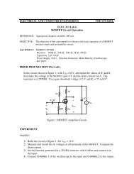
1. Given a 1-to-2 binary decoder with input I, active low enable E, and active low<br />
outputs Y:<br />
a. Draw the logic symbol and label all signals.<br />
b. Fill in a truth table (using don’t cares where appropriate).<br />
c. Write a VHDL entity (using std_logic_vectors where appropriate).<br />
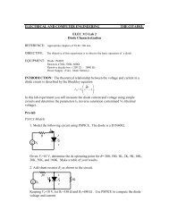
2. Implement the following function using a 4-to-1 multiplexer:<br />
F(w,x,y,z) = Σm(3,4,5,7,10,14) + Σd(1,6,8,15)<br />
3. Determine the ROM size and contents to implement the function for the square of the<br />
integers from 0 to 8.<br />
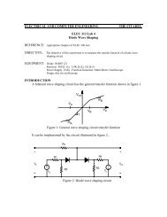
4. Given the following VHDL model, draw the schematic diagram (label completely).<br />
entity MUX4 is<br />
port (D : in std_logic_vector(3 downto 0);<br />
S : in std_logic_vector(1 downto 0);<br />
Y : out std_logic);<br />
end MUX4;<br />
architecture STRUCTURE of MUX4 is<br />
signal YD : std_logic_vector(1 downto 0);<br />
component MUX2<br />
port (D : in std_logic_vector(1 downto 0);<br />
S : in std_logic;<br />
Y : out std_logic);<br />
end component;<br />
begin<br />
M1 : MUX2 port map (D(3), D(2), S(0), YD(1));<br />
M2 : MUX2 port map (D(1), D(0), S(0), YD(0));<br />
M3 : MUX2 port map (YD(1), YD(0), S(1), Y);<br />
end STRUCTURE;<br />
5. Design a synchronous circuit that implements a 3-bit modulo-6 counter<br />
(000, 001, ... , 101, 000, ... ):<br />
a. Fill in a transition table (use don’t cares for undefined next states).<br />
b. Minimize the next state (D FF) equations using Karnaugh maps.