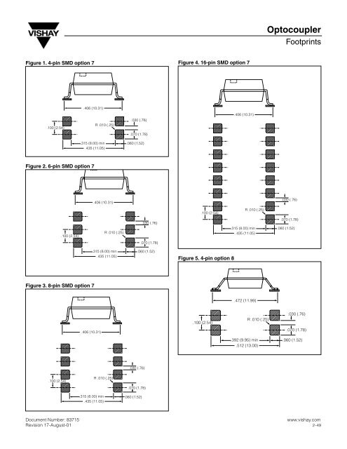
Optocoupler
Optocoupler
Optocoupler

You also want an ePaper? Increase the reach of your titles
YUMPU automatically turns print PDFs into web optimized ePapers that Google loves.
<strong>Optocoupler</strong><br />
Footprints<br />
Figure 1. 4-pin SMD option 7<br />
Figure 4. 16-pin SMD option 7<br />
.406 (10.31)<br />
.100 (2.54)<br />
R .010 (.25)<br />
.030 (.76)<br />
.406 (10.31)<br />
.070 (1.78)<br />
.315 (8.00) min .060 (1.52)<br />
.435 (11.05)<br />
Figure 2. 6-pin SMD option 7<br />
.406 (10.31)<br />
.030 (.76)<br />
.100 (2.54)<br />
R .010 (.25)<br />
.100 (2.54)<br />
R .010 (.25)<br />
.030 (.76)<br />
.315 (8.00) min<br />
.435 (11.05)<br />
.070 (1.78)<br />
.060 (1.52)<br />
.070 (1.78)<br />
.315 (8.00) min<br />
.435 (11.05)<br />
.060 (1.52)<br />
Figure 5. 4-pin option 8<br />
Figure 3. 8-pin SMD option 7<br />
.472 (11.99)<br />
.100 (2.54)<br />
R .010 (.25)<br />
.030 (.76)<br />
.406 (10.31)<br />
.070 (1.78)<br />
.392 (9.95) min .060 (1.52)<br />
.512 (13.00)<br />
.030 (.76)<br />
.100 (2.54)<br />
R .010 (.25)<br />
.070 (1.78)<br />
.315 (8.00) min<br />
.435 (11.05)<br />
.060 (1.52)<br />
Document Number: 83715<br />
www.vishay.com<br />
Revision 17-August-01 2–49
Figure 6. 6-pin option 8<br />
Figure 9. 8-pin SMD option 9<br />
.472 (11.99)<br />
.395 (10.03)<br />
.030 (.76)<br />
.100 (2.54)<br />
R .010 (.25)<br />
.392 (9.95) min<br />
.512 (13.00)<br />
.070 (1.78)<br />
.060 (1.52)<br />
.100 (2.54)<br />
R .010(.25)<br />
.030 (.76)<br />
.070 (1.78)<br />
Figure 7. 4-pin SMD option 9<br />
.315 (8.00) min<br />
.435 (11.05)<br />
.060 (1.52)<br />
Figure 10. 16-pin SMD option 9<br />
.395 (10.03)<br />
.100 (2.54)<br />
R .010(.25)<br />
.030 (.76)<br />
.395 (10.03)<br />
.070 (1.78)<br />
.315 (8.00) min<br />
.435 (11.05)<br />
.060 (1.52)<br />
Figure 8. 6-pin SMD option 9<br />
.395 (10.03)<br />
.030 (.76)<br />
.030 (.76)<br />
.100 (2.54)<br />
R .010(.25)<br />
.070 (1.78)<br />
.100 (2.54)<br />
R .010(.25)<br />
.315 (8.00) min<br />
.435 (11.05)<br />
.060 (1.52)<br />
.070 (1.78)<br />
.315 (8.00) min<br />
.435 (11.05)<br />
.060 (1.52)<br />
Document Number: 83715<br />
www.vishay.com<br />
Revision 17-August-01 2–50
Figure 11. 8-pin PCMCIA<br />
Figure 14. 16-pin PCMCIA<br />
R .010(.25)<br />
.336 (8.53)<br />
.336 (8.53)<br />
.050 (1.27)<br />
.014 (.36)<br />
.036 (.91)<br />
.266 (6.76) .045 (1.14)<br />
.356 (9.04)<br />
R .010(.25)<br />
.100 (2.54)<br />
Figure 12. 4-pin MINI-FLAT<br />
.050 (1.27)<br />
.014 (.36)<br />
.036 (.91)<br />
.266 (6.76) .045 (1.14)<br />
.356 (9.04)<br />
R .010 (.25)<br />
.270 (6.86)<br />
.014 (.36)<br />
Figure 15. 8-pin PCMCIA, heatsink<br />
.100 (2.54)<br />
.036 (.91)<br />
.200 (5.08) .045 (1.14)<br />
.290 (7.37)<br />
.336 (8.53)<br />
R .010(.25)<br />
Figure 13. 16-pin MINI-FLAT<br />
.050 (1.27)<br />
.086 (2.18)<br />
.014 (.36)<br />
.036 (.91)<br />
.266 (6.76) .045 (1.14)<br />
.356 (9.04)<br />
R .010 (.25)<br />
.270 (6.86)<br />
Figure 16. SO8A and DSO8A SMD<br />
.236 (5.99)<br />
.050 (1.27)<br />
.014 (.36)<br />
R .010 (.13)<br />
.036 (.91)<br />
.200 (5.08) .045 (1.14)<br />
.290 (7.37)<br />
.050 (1.27)<br />
.014 (.36)<br />
.036 (.91)<br />
.170 (4.32) .045 (1.14)<br />
.260 (6.6)<br />
Document Number: 83715<br />
www.vishay.com<br />
Revision 17-August-01 2–51
Figure 17. Mini coupler<br />
.276 (7.01)<br />
R .005(.13)<br />
.010 (.25)<br />
.053 (1.35)<br />
.050 (1.27)<br />
.040 (1.02)<br />
.216 (5.49)<br />
.296 (7.52)<br />
.024 (.61)<br />
.026 (.66)<br />
Document Number: 83715<br />
www.vishay.com<br />
Revision 17-August-01 2–52
<strong>Optocoupler</strong>s in Switching Power Supplies<br />
The following chapters should give a full<br />
understanding on how to use optocouplers which<br />
provide protection against electric shock for designs.<br />
Safety standards for optocouplers are intended to<br />
prevent injury or damage due to electric shock<br />
Two levels of electrical interface are normally used:<br />
Reinforced, or safe insulation is required in an<br />
optocoupler interface between a hazardous voltage<br />
circuit (like an ac line) and a touchable Safety Extra<br />
Low Voltage (SELV) circuit.<br />
Basic insulation is required in an optocoupler<br />
interface between a hazardous voltage circuit and a<br />
non-touchable Extra Low Voltage (ELV) circuit.<br />
The most widely used insulation for optocouplers in<br />
switch-mode power supply is reinforced insulation<br />
(class II). The following information enables the<br />
designer to understand the safety aspects, the basic<br />
concept of the VDE 0884 and the design<br />
requirements for applications.<br />
VDE 0884 - Facts and Information<br />
<strong>Optocoupler</strong>s for line-voltage separation must have<br />
several national standards. The most accepted<br />
standards are:<br />
D<br />
D<br />
D<br />
D<br />
UL/ CSA for America<br />
BSI for Great Britain<br />
FIMKO, SEMKO, NEMKO, DEMKO for Nordic<br />
countries (Europe)<br />
VDE for Germany<br />
Today, most manufacturers operate on a global<br />
scale. It is therefore mandatory to perform all<br />
approvals.<br />
The VDE 0884 is becoming a major safety standard<br />
in the world, partly due to German experts having a<br />
long record of experience in this field. It is therefore<br />
worthwhile understanding some requirements and<br />
methods of the VDE 0884.<br />
At the moment there is the drafts which is being<br />
circulated to set the VDE 0884 to an international IEC<br />
standard: IEC 47C / 199 / CD ; after voting, this draft<br />
will be a part of IEC 747-5.<br />
If design engineers work with VISHAY optocouplers,<br />
they will find some terms and definitions in the data<br />
sheets which relate to VDE 0884. These will now be<br />
explained:<br />
Rated isolation voltages:<br />
Vishay Telefunken<br />
V IO is the voltage between the input terminals and the<br />
output terminals.<br />
Note: All voltages are peak voltages!<br />
D V IOWM is a maximum rms. voltage value of the<br />
optocouplers assigned by VISHAY. This<br />
characterizes the long term withstand capability<br />
of its insulation.<br />
D V IORM is a maximum recurring peak (repetitive)<br />
voltage value of the optocoupler assigned by<br />
VISHAY. This characterizes the long-term<br />
withstand capability against recurring peak<br />
voltages.<br />
D V IOTM is an impulse voltage value of the<br />
optocoupler assigned by VISHAY. This<br />
characterizes the long-term withstand capability<br />
against transient over voltages.<br />
Isolation test voltage for routine tests is at factor<br />
1.875 higher than the specified V IOWM / V IORM (peak).<br />
A partial discharge test is a different test method to<br />
the normal isolation voltage test. This method is more<br />
sensitive and will not damage the isolation behavior<br />
of the optocoupler like other test methods probably<br />
do.<br />
The VDE 0884 therefore does not require a minimum<br />
thickness through insulation. The philosophy is that<br />
a mechanical distance only does not give you an<br />
indication of the safety reliability of the coupler. It is<br />
more recommendable to check the total construction<br />
together with the assembling performance. The<br />
partial discharge test method can monitor this<br />
more reliably.<br />
The following tests must be done to guarantee this<br />
safety requirement.<br />
100% test (piece by piece) for one second at a<br />
voltage level of specified V IOWM /V IORM (peak)<br />
multiplied by 1.875 * test criteria is partial discharge<br />
less than 5 pico coulomb.<br />
A lotwise test at V IOTM for 10 seconds and at a<br />
voltage level of specified V IOWM / V IORM (peak)<br />
multiplied by 1.5 for 1 minute * test criteria is partial<br />
discharge less than 5 pico coulomb.<br />
Design example:<br />
The line ac voltage is 380 V rms. Your application<br />
class is III (DIN/VDE 0110 Part 1/1.89). According to<br />
table 1, you must calculate with a maximum line<br />
voltage of 600 V and a transient over voltage of<br />
6000 V.<br />
03.99 1
Vishay Telefunken<br />
Table 1.<br />
Recommended transient overvoltages related to ac/ dc line voltage (peak values)<br />
V IOWM /V IORM<br />
up to<br />
Appl. Class I Appl. Class II Appl. Class III Appl. Class IV<br />
50 V 350 V 500 V 800 V 1500 V<br />
100 V 500.V 800 V 1500 V 2500 V<br />
150 V 800 V 1500 V 2500 V 4000 V<br />
300 V 1500 V 2500 V 4000 V 6000 V<br />
600 V 2500 V 4000 V 6000 V 8000 V<br />
1000 V 4000 V 6000 V 8000 V 12000 V<br />
Now select the TCDT1100 from our VISHAY coupler<br />
program. The next voltage step of 380 V is 600 V<br />
(V IOWM ).The test voltages are 1600 V for the<br />
TCDT1100 for the routine test and 6000 V/ 1300 V for<br />
the sample test.<br />
The VDE 0884 together with the isolation test<br />
voltages also require very high isolation resistance,<br />
tested at an ambient temperature of 100°C.<br />
Apart from these tests for the running production, the<br />
VDE Testing and Approvals Institute also<br />
investigates the total construction of the optocoupler.<br />
The VDE 0884 requires life tests in a very special<br />
sequence; 5 lots for 5 different subgroups are tested.<br />
The sequence for the main group is as follows:<br />
D<br />
D<br />
D<br />
D<br />
D<br />
D<br />
D<br />
D<br />
Cycle test<br />
Vibration<br />
Shock<br />
Dry heat<br />
Accelerated damp heat<br />
Low temperature storage (normally --55°C)<br />
Damp heat steady state<br />
Final measurements.<br />
Finally there is another chapter concerning the safety<br />
ratings. This is described in VDE 0884.<br />
The maximum safety ratings are the electrical,<br />
thermal and mechanical conditions that exceed the<br />
absolute maximum ratings for normal operations.<br />
The philosophy is that optocouplers must withstand<br />
a certain exceeding of the input current, output power<br />
dissipation, and temperature for at least a weekend.<br />
The test time is actually 72 hours. This is a simulated<br />
space of time where failures may occur.<br />
It is the designer’s task to create his design inside of<br />
the maximum safety ratings.<br />
<strong>Optocoupler</strong>s -- approved to the VDE 0884 -- must<br />
consequently pass all tests undertaken. This then<br />
enables you to go ahead and start your design.<br />
Layout Design Rules<br />
The previous chapter described the important safety<br />
requirements for the optocoupler itself; but the<br />
knowledge of the creepage distance and clearance<br />
path is also important for the design engineer if the<br />
coupler is to be mounted onto the circuit board.<br />
Although several different creepage distances<br />
referring to different safety standards, like the IEC 65<br />
for TV or the IEC 950 for office equipment, computer,<br />
data equipment etc. are requested, there is one<br />
distance which meanwhile dominates switching<br />
power supplies: This is the 8 mm spacing<br />
requirement between the two circuits: The hazardous<br />
input voltage (ac 240 power-line voltage) and the<br />
safety low voltage.<br />
This 8 mm spacing is related to the 250 V power line<br />
and defines the shortest distance between the<br />
conductive parts (either from the input to the output<br />
leads) along the case of the optocoupler, or across<br />
the surface of the print board between the solder<br />
eyes of the optocoupler input/ output leads, as shown<br />
in figure 1. The normal distance input to output leads<br />
of an optocoupler is 0.3”. This is too tight for the 8 mm<br />
requirement. The designer now has two options: He<br />
can provide a slit in the board, but then the airgap is<br />
still lower; or he can use the ”G” optocoupler from<br />
VISHAY. ”G” stands for a wide-spaced lead form of<br />
0.4” and obtains the 8 mm creepage, clearance<br />
distance. The type designation for this type of ”G”<br />
coupler is, for example: TCDT1100G.<br />
The spacing requirements of the 8 mm must also be<br />
taken into consideration for the layout of the board.<br />
Figures 2 and 3 provide examples for your layout.<br />
The creepage distance is also related to the<br />
resistance of the tracking creepage current stability.<br />
The plastic material of the optocoupler itself and the<br />
2<br />
03.99
Vishay Telefunken<br />
material of the board must provide a specified<br />
creeping-current resistance.<br />
The behavior of this resistance is tested with special<br />
test methods described in the IEC 112. The term is<br />
”CTI” (Comparative Tracking Index).<br />
The VDE 0884 requires a minimum of a CTI of 175.<br />
Creepage<br />
path<br />
Clearance path<br />
Figure 1. Isolation creepage/ clearance path along the body<br />
(The creepage path is the shortest distance between conductive parts along the surface of the isolation<br />
material. The clearance path is the shortest distance between conductive parts.)<br />
0.4 ”/ 10.16 mm<br />
0.332 ”/ 8.2 mm<br />
Figure 2. Isolation creepage/ clearance path after mounting on a board (side view)<br />
03.99 3
Vishay Telefunken<br />
Power interface area<br />
G<br />
G = 0.322 ” / 8.2 mm<br />
Layer<br />
SELV control circuit area<br />
Power interface area<br />
G<br />
G<br />
G<br />
SELV control circuit area<br />
Figure 3. ”Top view of optocoupler mounting on a board”<br />
(clearance on PC board: 0.322 / 8.2 mm, creepage path on PC board is 0.322 / 8.2 mm)<br />
Not only the solder eyes of the coupler itself on the board must have the 8 mm distance, but also all<br />
layers located between the SELV areas and the power interface areas.<br />
VISHAY <strong>Optocoupler</strong> Program<br />
Construction<br />
An optocoupler is comparable with a transformer or<br />
a mechanical relay; but its advantages are smaller<br />
dimensions, shorter switching time, no contact<br />
bounces, no interference caused by arcs and the<br />
possibility of adapting a signal already in the coupler<br />
for the following stage of the circuit.<br />
This combination together with the safety aspects<br />
provides outstanding advantages for use in power<br />
supplies. Safety factors in particular depend on the<br />
design, construction and selected materials. VISHAY<br />
optocouplers are designed with a coplanar lead<br />
frame, where the die are mounted side by side. A<br />
semi-ellipsoid with even better reflection capabilities<br />
is fitted over each dice. The entire system is then<br />
casted in a plastic material impermeable to the<br />
infrared range and of high di-electric strength. The<br />
whole system is now molded with a special mold<br />
compound to ensure that no external influences such<br />
as light or dust etc. interfere with the functioning of the<br />
coupler (see figure LEERER MERKER). This design<br />
has several advantages: The ”thickness through<br />
insulation”, the clearance (internally) between the<br />
input and the output side is fixed at 0.75 mm and is<br />
thus mechanically stable even under thermal<br />
overloads, i.e., the possibility of a short circuit caused<br />
by material deformation is excluded. Deviations of<br />
this distance during the production process are also<br />
excluded. These two features are the specific<br />
reasons why VISHAY optocouplers are<br />
well-accepted by manufacturers of power supplies.<br />
1.) External Creepage Distance<br />
2.) Internal Creepage Distance >4mm<br />
3.) 0.75 mm fixed thickness--through--insulation<br />
4.) Clearance path<br />
Figure 4. Coplanar construction (e.g., CQY80N)<br />
4<br />
03.99
Vishay Telefunken<br />
Overview<br />
The information given in this brochure enables the<br />
designer to select the right optocoupler for his<br />
application. The previous chapters focused only on<br />
safety aspects. Apart from this there are other<br />
characteristics for the optocoupler. Table 2 enables<br />
the designer to select the optocoupler to suit his own<br />
needs. This selection should be done using the most<br />
important characteristics like CTR (Current Transfer<br />
Ratio) and devices with or without base connection.<br />
The designer may ask for our data sheets for detailed<br />
information.<br />
n.c. C E<br />
6 5 4<br />
B<br />
C<br />
E<br />
6 5 4<br />
6 -PIN STD Isolators<br />
Table 2. Devices offering (VDE 0884-tested)<br />
1 2 3<br />
A (+) C ( -) n.c.<br />
Without base connection<br />
1 2 3<br />
A (+) C ( -) n.c.<br />
With base connection<br />
CTR<br />
IC/ IF<br />
Base<br />
Connection<br />
> 20% 4N25(G)V<br />
V CE > 32 V<br />
Ungrouped CTR<br />
V CE > 50 V<br />
Grouped CTR<br />
V CE > 90 V<br />
Grouped CTR<br />
With Without With Without With Without<br />
> 50% CQY80N(G) TCDT1100(G) TCDT1120(G)<br />
> 100% 4N35(G)V TCDT1110(G)<br />
40 -- 80% CNY17(G)--1 TCDT1101(G)<br />
63 -- 125% CNY17(G)--2 TCDT1102(G) CNY75(G)A TCDT1122(G)<br />
100 --<br />
200%<br />
160 --<br />
320%<br />
G = wide space 0.4” lead form, for 8 mm PC board spacing requirements<br />
CNY17(G)--3 TCDT1103(G) CNY75(G)B TCDT1123(G)<br />
CNY17(G)--4 CNY75(G)C TCDT1124(G)<br />
Appendix<br />
Approvals List<br />
As mentioned before, as long there is no equivalent<br />
IEC--standard to the VDE 0884, optocouplers must<br />
still fulfill all other national safety standards. The<br />
copies of documents present all certificates the<br />
designer needs for worldwide acceptance of his<br />
power supply (see ANT018). All the approvals below<br />
are most important. If the designer needs any others,<br />
he must be aware that there are many agreements<br />
between national institutes, e.g., UL for USA is also<br />
accepted by CSA/Canada.<br />
VISHAY divides optocouplers into ”coupling<br />
systems”. Each coupling system represents the<br />
same technology, materials etc. The coupling<br />
systems are indicated with capital letters and each<br />
coupler is marked with this coupling system indicator<br />
letter. The certificates at least also refer to the<br />
systems and list all subtypes to the related coupling<br />
system. The user is able to find his selected coupler<br />
on the certificate.<br />
03.99 5
Vishay Telefunken<br />
Safety Standard Approval List<br />
UL CSA VDE BSI NORDIC Std.<br />
Part Numbers<br />
UL<br />
1577 -<br />
single<br />
Protection<br />
UL<br />
1577 -<br />
double<br />
Protection<br />
C -UL<br />
1577-<br />
double<br />
Protection<br />
Safety standard according to<br />
VDE 0884<br />
IEC950/ EN60950;<br />
IEC65/ EN60065<br />
BSI<br />
EN60950<br />
(BS 7002/<br />
IEC950)<br />
BSI<br />
EN60065<br />
(BS 415/<br />
IEC65)<br />
FIMKO<br />
EN60950/ IEC950,<br />
EN60065/ IEC65<br />
Creepage<br />
Distance<br />
Thickness<br />
of<br />
Insulation<br />
A, C, H, J, K, U U A+C H, J, K U A, C, H, J, K, U A C U<br />
Inter-<br />
Exter-<br />
nal<br />
nal<br />
Coupling Systems 1)<br />
File Numbers<br />
E--76222 Card A+B 094778 076814 115667 7402 7081 12399 12398 11027 11992 mm mm mm<br />
4N25 up to 4N37 ¯ ¯ ¯ ¯ ¯ >4,0 6.0 0.75<br />
4N25GV ¯ ¯ ¯ ¯ ¯ ¯ >4,0 8.0 0.75<br />
4N25V ¯ ¯ ¯ ¯ ¯ ¯ >4,0 6.0 0.75<br />
4N32/ 4N33 ¯ ¯ ¯ ¯ ¯ >4,0 6.0 0.75<br />
4N33V ¯ ¯ ¯ ¯ ¯ ¯ >4,0 6.0 0.75<br />
4N35GV ¯ ¯ ¯ ¯ ¯ ¯ >4,0 8.0 0.75<br />
4N35V ¯ ¯ ¯ ¯ ¯ ¯ >4,0 6.0 0.75<br />
CNY17 -Series ¯ ¯ ¯ ¯ ¯ ¯ >4,0 6.0 0.75<br />
CNY17G -Series ¯ ¯ ¯ ¯ ¯ ¯ >4,0 8.0 0.75<br />
CNY64 -Series ¯ ¯ >4,0 9.0 >3,0<br />
CNY65 -Series ¯ ¯ >4,0 14.0 >3,0<br />
CNY65EXI ¯ ¯ >4,0 14.0 >3,0<br />
CNY66 ¯ ¯ >4,0 17.0 >3,0<br />
CNY74 -2H/ CNY74 -4H ¯ ¯ >4,0 6.0 0.75<br />
CNY75 -Series ¯ ¯ ¯ ¯ ¯ ¯ >4,0 6.0 0.75<br />
CNY75G -Series ¯ ¯ ¯ ¯ ¯ ¯ >4,0 8.0 0.75<br />
CQY80N ¯ ¯ ¯ ¯ ¯ ¯ >4,0 6.0 0.75<br />
CQY80NG ¯ ¯ ¯ ¯ ¯ ¯ >4,0 8.0 0.75<br />
K1150PG ¯ ¯ ¯ ¯ ¯ ¯ >4,0 8.0 0.75<br />
K3010P -Series ¯ ¯ ¯ ¯ ¯ ¯ >4,0 6.0 0.75<br />
K3010PG -Series ¯ ¯ ¯ ¯ ¯ ¯ >4,0 8.0 0.75<br />
K3020P -Series ¯ ¯ ¯ ¯ ¯ ¯ >4,0 6.0 0.75<br />
K3020PG -Series ¯ ¯ ¯ ¯ ¯ ¯ >4,0 8.0 0.75<br />
K814P/ K824P/ K844P ¯ ¯ ¯ >4,0 6.0 0.75<br />
K815P/ K825P/ K845P ¯ ¯ ¯ >4,0 6.0 0.75<br />
K817P -Series ¯ ¯ ¯ >4,0 6.0 0.75<br />
K827PH/ K847PH ¯ ¯ ¯ >4,0 6.0 0.75<br />
MCT6H/ MCT62H ¯ ¯ ¯ >4,0 6.0 0.75<br />
TCDT1100 Series ¯ ¯ ¯ ¯ ¯ ¯ >4,0 6.0 0.75<br />
TCDT1100G Series ¯ ¯ ¯ ¯ ¯ ¯ >4,0 8.0 0.75<br />
TCDT1110 ¯ ¯ ¯ ¯ ¯ ¯ >4,0 6.0 0.75<br />
TCDT1110G ¯ ¯ ¯ ¯ ¯ ¯ >4,0 8.0 0.75<br />
TCDT1120 Series ¯ ¯ ¯ ¯ ¯ ¯ >4,0 6.0 0.75<br />
TCDT1120G Series ¯ ¯ ¯ ¯ ¯ ¯ >4,0 8.0 0.75<br />
TCED1100 -TCED4100 ¯ ¯ ¯ ¯ ¯ ¯ ¯ >4,0 6.0 0.75<br />
TCED1100G -<br />
TCED4100G<br />
¯ ¯ ¯ ¯ ¯ ¯ ¯ >4,0 8.0 0.75<br />
TCET1100 -TCET4100 ¯ ¯ ¯ ¯ ¯ ¯ ¯ >4,0 6.0 0.75<br />
TCET1100G -<br />
TCET4100G<br />
¯ ¯ ¯ ¯ ¯ ¯ ¯ >4,0 8.0 0.75<br />
TCET1600 -TCET4600 ¯ ¯ ¯ ¯ ¯ ¯ ¯ >4,0 6.0 0.75<br />
TCET1600G -<br />
TCET4600G<br />
¯ ¯ ¯ ¯ >4,0 8.0 0.75<br />
1) Coupling Systems: Each coupling system represents the same technology, materials etc. The coupling<br />
systems are indicated with capital letters an each coupler is marked with this coupling system indicator letter.<br />
The bold certificates at least also refer to the systems and list all subtypes to the related coupling system. The<br />
user is able to track his selected coupler on the certificate.<br />
6<br />
03.99
Vishay Telefunken<br />
General Description<br />
Basic Function<br />
In an electrical circuit, an optocoupler ensures total<br />
electric isolation, including potential isolation, as in<br />
the case of a transformer, for instance.<br />
In practice, this means that the control circuit is<br />
located on one side of the optocoupler, i.e., the<br />
emitter side, while the load circuit is located on the<br />
other side, i.e., the receiver side. Both circuits are<br />
electrically isolated by the optocoupler (figure 5).<br />
Signals from the control circuit are transmitted<br />
optically to the load circuit, and are therefore free of<br />
retroactive effects. In most cases, this optical<br />
transmission is realized with light beams whose<br />
wavelengths span the red to infrared range,<br />
depending on the requirements applicable to the<br />
optocoupler. The bandwidth of the signal to be<br />
transmitted ranges from a dc voltage signal to<br />
frequencies in the MHz band. An optocoupler is<br />
comparable to a transformer or relay. Besides having<br />
smaller dimensions in most cases, the advantages of<br />
optocouplers compared to relays are the following: it<br />
ensures considerably shorter switching times, no<br />
contact bounce, no interference caused by arcs, no<br />
mechanical wear and the possibility of adapting a<br />
signal, already in the coupler, to the following stage<br />
in the circuitry. Thanks to all these advantages,<br />
optocouplers are outstandingly suitable for circuits<br />
used in microelectronics and also in data processing<br />
and telecommunication systems. <strong>Optocoupler</strong>s are<br />
used to an increasing extent as safety tested<br />
components, e. g., in switchmode power supplies.<br />
Design<br />
An optocoupler has to fulfill 5 essential requirements:<br />
D<br />
D<br />
D<br />
D<br />
D<br />
Good insulation behavior<br />
High current transfer ratio (CTR)<br />
Low degradation<br />
Low coupling capacitance<br />
No uncontrolled function by field strength<br />
influences<br />
These factors are essentially dependent on the<br />
design, the materials used and the corresponding<br />
chips used for the emitter/receiver.<br />
Vishay has succeeded in achieving a design with<br />
optimized insulation behavior and good transfer<br />
characteristics with their Co--planar technology.The<br />
basic function of an optocoupler is to isolate the input<br />
from the output by means of an insulation material.<br />
In most optocouplers, the emitter and detector chips<br />
face each other on seperate lead frames. As a result,<br />
the distance between these two chips may vary,<br />
causing reliability problems. TELEFUNKEN’S<br />
co--planar technology ensures that there is a stable<br />
distance between the emitter and detector chips. The<br />
fixed thickness--through--insulation of 0.75 mm<br />
provided by TELEFUNKEN’S co--planar<br />
optocouplers is larger than competing devices and<br />
provides better safety and protection against<br />
electrical shock (see figure 1/2).TELEFUNKEN<br />
builds in additional reliability to these devices by using<br />
a special white molding compound to protect the<br />
coupler system against ambient light and dust. This<br />
solution does not require an additional internal<br />
reflector any longer.<br />
The mechanical clearance between the emitter and<br />
receiver is 0.75 mm and is thus mechanically stable<br />
even under thermal overloads, i.e., the possibility of<br />
a short circuit caused by material deformation is<br />
excluded. This is important for optocouplers which<br />
have to fulfill strict safety requirements (VDE/UL<br />
specifications), see VDE0884 Facts and Information.<br />
Thanks to their large clearance these couplers have<br />
a very low coupling capacity of 0.2 pF. Couplers with<br />
conventional designs, i.e., where the emitter and<br />
receiver are fitted ”face-to-face”(see figure 2), have<br />
higher coupling capacitance values by a factor of 1.3<br />
- 2. Attention must be paid to the coupling<br />
capacitance in digital circuits in which steep pulse<br />
edges are produced which superimpose themselves<br />
on the control signal. With a low coupling<br />
capacitance, the transmission capabilities of these<br />
interference spikes are effectively suppressed<br />
between the input and output because a coupler<br />
should only transmit the effective signal. This<br />
capability of suppressing dynamic interferences is<br />
commonly known as “common-mode rejection”.<br />
03.99 1
Vishay Telefunken<br />
1.) External Creepage Distance<br />
2.) Internal Creepage Distance >4mm<br />
3.) 0.75 mm fixed thickness--through--insulation<br />
4.) Clearance path<br />
Figure 1. Coplanar Construction Principle<br />
(e.g., CQY80N)<br />
potential. The manufacturer should create suitable<br />
protective measures in this case. Using Vishay’s<br />
optocouplers, such protective measures are not<br />
necessary thanks to their perfect design.<br />
The degradation of an optocoupler, i.e., impairment<br />
of its CTR over a finite period, depends on two<br />
factors. On the one hand, it depends on the emitter<br />
element due to its decreasing radiation power while,<br />
on the other hand, it depends on ageing or<br />
opaqueness of the synthetic resin which must<br />
transmit the radiation from the emitter to the receiver.<br />
A decrease in the radiation power can be primarily<br />
ascribed to thermal stress caused by an external,<br />
high ambient temperature and/or high a forward<br />
current. In practice, optocouplers are operated with<br />
forward current of 1 to 30 mA through the emitting<br />
diode. In this range, degradation at an average<br />
temperature of 40°C is less than 5% after 1000 h. In<br />
general, an optocoupler’s life time is a period of<br />
100.000 h, i.e, the CTR should not have dropped<br />
below 50% of its value at 0 hours during this time (see<br />
figure 9).<br />
Figure 3. Functions of parasitic field effect transistor as a<br />
result of failure (latch-up) in the<br />
phototransistor of couplers<br />
Figure 2.<br />
Face to Face Construction Principle<br />
Due to the special design of these couplers, the<br />
receiver surface is outside the area of the direct field<br />
strength. Field strength is produced when there is a<br />
voltage potential between the coupler’s input and<br />
output. It causes the migration of positive ions to the<br />
transistor’s surface. Positive ions perform on the<br />
base in the same way as a gate voltage applied to an<br />
n-channel FET transistor (see figure 8).<br />
If inversions occur on the surface, the phototransistor<br />
becomes forward-biased, causing an inadmissible<br />
residual collector-emitter current. As a result,<br />
controlled functioning of the coupler is no longer<br />
guaranteed (figure 8). This effect occurs mainly<br />
whenever the receiver is within the field strength<br />
Average Percent of Initial CTR<br />
15918<br />
100<br />
90<br />
80<br />
70<br />
60<br />
50<br />
40<br />
30<br />
20<br />
10<br />
0<br />
Leadership in IR technology<br />
D The die’s molecular structure<br />
D Mesa technology<br />
D Special bond layout results in an<br />
homogenuous current distribution<br />
D Special rear metalization<br />
0 20000 40000 60000 80000 100000<br />
Life Test Hours<br />
Figure 4. Degradation under typical operating<br />
conditions with reference to the CQY80N<br />
T j = 65°C<br />
I F = 60mA<br />
T j = 125°C<br />
I F = 60mA<br />
2<br />
03.99
Vishay Telefunken<br />
Technical Description -<br />
Assembly<br />
Emitter<br />
Emitters are manufactured using the most modern<br />
Liquid Phase Epitaxy (LPE) process. By using this<br />
technology, the number of undesirable flaws in the<br />
crystal is reduced. This results in a higher quantum<br />
efficiency and thus higher radiation power.<br />
Distortions in the crystal are prevented by using<br />
mesa technology which leads to lower degradation.<br />
A further advantage of the mesa technology is that<br />
each individual chip can be tested optically and<br />
electrically even on the wafer.<br />
Detector<br />
Vishay detectors have been developed so that they<br />
match perfectly to the emitter. They have low<br />
capacitance values, high photosensitivity and are<br />
designed for an extremely low saturation voltage.<br />
Silicon nitride passivation protects the surface<br />
against possible impurities.<br />
Assembly<br />
The components are fitted onto lead frames by fully<br />
automatic equipment using conductive epoxy<br />
adhesive. Contacts are established automatically<br />
with digital pattern recognition using the well-proven<br />
thermosonic technique. In addition to optical and<br />
mechanical checks, all couplers are measured at a<br />
temperature of 100°C on a short/open<br />
testequipment.<br />
Conversion Tables - Optoelectronic General<br />
Table 1. Corresponding radiometric and photometric definitions, symbols and units (DIN 5031, Part 1, 3)<br />
Radiometric Units<br />
Photometric Units<br />
Unit Symbol Unit Unit Symbol Unit<br />
Note<br />
Radiant flux, F e Watt, W Luminous flux F v lumen, lm Power<br />
Radiant power<br />
Radiant exitance,<br />
Exitance<br />
M e W/m 2 Luminous emittance M v lm/m 2 Output power per<br />
unit area<br />
(Radiant) intensity I c W/sr (Luminous) intensity I v Candela,<br />
cd, lm/sr<br />
Output power per<br />
unit solid angle<br />
Radiant sterance, L e<br />
Luminance<br />
L v cd/m 2 Output power per<br />
Radiance<br />
W (Brightness sterance)<br />
unit solid angle<br />
sr * m 2<br />
and emitting areas<br />
Radiant incidance,<br />
Irradiance<br />
E e W/m 2 Illuminance E v lm/m 2<br />
Lux, lx<br />
Input power per<br />
unit area<br />
Radiant energy Q e Ws Luminous energy Q v lm s Power time<br />
Irradiation H e Ws/m 2 Illumination H v lm s/m 2 Radiant energy or<br />
luminous energy<br />
per unit area<br />
03.99 3
Vishay Telefunken<br />
Measurement Techniques<br />
Introduction<br />
The characteristics given in the optocoupler‘s data<br />
sheets are verified either by 100% production tests<br />
followed by statistic evaluation or by sample tests on<br />
typical specimens. Possible tests are the following:<br />
Measurements on emitter chip<br />
Measurements on detector chip<br />
Static measurements on optocoupler<br />
Measurement of switching characteristics, cut-off<br />
frequency and capacitance<br />
Thermal measurements<br />
The basic circuits used for the most important<br />
measurements are shown in the following sections,<br />
although these circuits may be modified slightly to<br />
cater for special measurement requirements.<br />
Measurements on Emitter Chip<br />
Forward- and Reverse Voltage<br />
Measurements<br />
The forward voltage, V F, is measured either on a<br />
curve tracer or statically using the circuit shown in<br />
figure 10. A specified forward current (from a<br />
constant current source) is passed through the<br />
device and the voltage developed across it is<br />
measured.<br />
To measure the reverse voltage, V R , a 10 A reverse<br />
current from a constant current source is applied to<br />
the diode (figure 11) and the voltage developed<br />
across it is measured on a voltmeter of extremely<br />
high input impedance (≥10 M).<br />
V S = 5 V<br />
I = 50 mA<br />
100 mA<br />
constant<br />
V F<br />
V<br />
Figure 1.<br />
V S = 80 V<br />
( > V R max )<br />
V R<br />
I = 10 A<br />
constant<br />
V<br />
R i > 10 k<br />
94 8205<br />
R i > 10 M<br />
94 8206<br />
Figure 2.<br />
03.99 1
Vishay Telefunken<br />
Measurements on Detector Chip<br />
V CEO and I CEO Measurements<br />
The collector-emitter voltage, V CEO , is measured<br />
either on a transistor curve tracer or statically using<br />
the circuit shown in figure 12.<br />
The collector dark current, I CEO , must be measured<br />
in complete darkness (figure 13). Even ordinary<br />
daylight illumination might cause wrong<br />
measurement results.<br />
V S = 100 V<br />
( > V CEO )<br />
I C =1mA<br />
constant<br />
Static Measurements<br />
To measure the collector current, I C (figure 14), a<br />
specified forward current, I F , is applied to the lR<br />
diode. Voltage drop is then measured across a low<br />
emitter resistance.<br />
In the case of collector-emitter saturation voltage,<br />
V CEsat (figure 15), a forward current, I F , is applied to<br />
the IR diode and a low collector current, I C , in the<br />
phototransistor. V CEsat is then measured across<br />
collector and emitter terminals.<br />
V S = 5 V<br />
I F = 5mA<br />
10 mA<br />
constant<br />
V S = 5 V<br />
I C<br />
E < 100 lx<br />
V CEO<br />
V<br />
R i 1M<br />
1<br />
mV<br />
R j = 10 k<br />
96 12367<br />
96 11696<br />
Figure 3.<br />
Figure 5.<br />
V S = 20 V<br />
V S = 5 V<br />
V S = 5 V<br />
E = 0<br />
I CEO<br />
I F = 10mA<br />
constant<br />
I C =1mA<br />
constant<br />
10 k mV<br />
R i = 1 M<br />
V CEsat<br />
V<br />
R j 1M<br />
96 11695<br />
94 8218<br />
Figure 4.<br />
Figure 6.<br />
2<br />
03.99
Vishay Telefunken<br />
Switching Characteristics<br />
Definition<br />
Each electronic device generates a certain delay<br />
between input and output signals as well as a certain<br />
amount of amplitude distortion. A simplified circuit<br />
(figure 16) shows how the input and output signals of<br />
optocouplers can be displayed on a dual-trace<br />
oscilloscope.<br />
V S<br />
Improvements of Switching<br />
Characteristics of Phototransistors<br />
and Darlington Phototransistors<br />
With normal transistors, switching tunes can be<br />
reduced if the drive signal level and hence the<br />
collector current is increased. Another time reduction<br />
(especially in fall time t f ) can be achieved by using a<br />
suitable base resistor. However, this can only be<br />
done at the expense of a decreasing CTR.<br />
I F<br />
96 11697<br />
GaAs-Diode<br />
Channel I<br />
Channel II<br />
Figure 7.<br />
The following switching characteristics can be<br />
determined by comparing the timing of the output<br />
current waveform to that of the input current<br />
waveform (figure 17).<br />
96 11698<br />
I F<br />
0<br />
t<br />
t p<br />
t p<br />
pulse duration<br />
t d<br />
delay time<br />
I C<br />
t r<br />
rise time<br />
t on (= t d + t r ) turn-on time<br />
100%<br />
t s<br />
storage time<br />
90%<br />
t f<br />
fall time<br />
t off (= t s + t f ) turn-off time<br />
10%<br />
0<br />
t r<br />
t d<br />
t on<br />
t s t f<br />
t<br />
Figure 8.<br />
t off<br />
03.99 3
Vishay Telefunken<br />
Cut-off Frequency Measurement<br />
The cut-off frequency is the frequency at which the coupler of the small signal current transfer ratio has<br />
decreased to 1 22<br />
of its lowest frequency value.<br />
50 Ω<br />
Channel A<br />
+V CC<br />
Channel B<br />
50 Ω R L<br />
GND<br />
Figure 9. Test circuit for cut-off frequency<br />
15941<br />
Coplanar 6 PIN e.g.: TCDT1100 Series<br />
Relative AC Output ( dB )<br />
5<br />
0<br />
–5<br />
–10<br />
–15<br />
–3 dB<br />
CTR=100%<br />
CTR=150%<br />
CTR=65%<br />
–20<br />
V CC =5V, I C =5mA,<br />
R L =100<br />
–25<br />
1 10 100 1000<br />
15943<br />
f – Frequency ( kHz )<br />
Figure 10. Rel. Current Transfer Ratio / Frequency<br />
Relative AC Output ( dB )<br />
5<br />
0<br />
–5<br />
–10<br />
–15<br />
–3 dB CTR=65%<br />
CTR=100%<br />
CTR=150%<br />
–20<br />
V CC =5V, I C =2mA,<br />
R L =1k<br />
–25<br />
1 10 100 1000<br />
15942<br />
f – Frequency ( kHz )<br />
Figure 11. Rel. Current Transfer Ratio / Frequency<br />
Before applying an AC test signal to the coupler<br />
input terminals , the IR diode has to be baised<br />
with a DC current in order to establish a work–<br />
point in the linear region of the phototransistor’s<br />
output diagram. Then a small sinusoidal current<br />
signal of 1000Hz is superimposed to the DC bais<br />
current. The output to input AC signal ratio i C /i F is<br />
measured and set to 0 dB. After this the<br />
frequency of the input signal is increased and the<br />
i C /i F ratio is recorded and plotted. Depending on<br />
the coupler’s DC current transfer ratio and the<br />
test conditions, the AC signal ratio will drop at<br />
higher frequency levels. The frequency value at<br />
–3 dB signal level is called the cut–off frequency.<br />
Coplanar 4 PIN e.g.: TCET1100 Series<br />
Relative AC Output ( dB )<br />
5<br />
0<br />
–5<br />
–10<br />
–15<br />
–3 dB<br />
CTR=100%<br />
CTR=180%<br />
CTR=65%<br />
–20<br />
V CC =5V, I C =5mA,<br />
R L =100<br />
–25<br />
1 10 100 1000<br />
15945<br />
f – Frequency ( kHz )<br />
Figure 12. Rel. Current Transfer Ratio / Frequency<br />
Relative AC Output ( dB )<br />
5<br />
0<br />
–5<br />
–10<br />
–15<br />
–3 dB CTR=65%<br />
CTR=100%<br />
CTR=180%<br />
–20<br />
V CC =5V, I C =2mA,<br />
R L =1k<br />
–25<br />
1 10 100 1000<br />
15944<br />
f – Frequency ( kHz )<br />
Figure 13. Rel. Current Transfer Ratio / Frequency<br />
4<br />
03.99
Application Examples<br />
<strong>Optocoupler</strong>s in IC Logic Design<br />
Two examples of dimensioning a TTL logic circuit<br />
employing an optocoupler, Series TCET110X or<br />
K817P.<br />
a) Supply voltage: V CC = 5 V<br />
b) Operation temperature range: –20°C to +60°C<br />
c) Service life of application: 10 years<br />
The following conditions are intended to apply to both<br />
examples conjointly:<br />
Example 1<br />
Phototransistor wired to emitter resistor.<br />
I F<br />
R V<br />
TTL<br />
Vishay Telefunken<br />
A voltage V L at R L resistor of V IH 2 V is<br />
necessary in order to attain a safe high state at the<br />
output. This needs to be generated by the collector<br />
current Ic of the phototransistor.<br />
In the case of the TTL output at the input of the optocoupler<br />
the current should remain I OL < = 16 mA.<br />
The CTR value of 50% results in maximum output<br />
current I C for the optocoupler of 8 mA.<br />
V CC<br />
V CC<br />
This allows the minimum value to be determined<br />
for R<br />
TCET1100 IC<br />
L .<br />
K817P<br />
R L V IH<br />
I L<br />
2V<br />
8mA 250 <br />
I IL I IH<br />
I If for example R L TTL<br />
L = 390 is selected and 20% safety<br />
is computed to the minimum V IH in respect of the high<br />
R L V L<br />
state (V IH + V IH 20% = 2.4 V), this will then permit<br />
15096<br />
I C , I F and the dropping resistor R V at the input of the<br />
optocoupler to be determined,<br />
I C I L 2.4 V 6.15 mA<br />
390 <br />
– I F <br />
6.15 mA<br />
12.3 mA<br />
CTR<br />
With V F = 1.2 V, (the forward voltage of the I R diode)<br />
and V OL < 0.4 V for the TTL output follows<br />
R V V CC –V F –V OL<br />
12.3 mA 276 , R V 270 <br />
For dimensioning purposes, a typical CTR value of<br />
100% at I F = 10 mA is selected. Within the<br />
temperature range of –20°C to +60°C the CTR<br />
undergoes change between +12% and –17% (see<br />
data sheet). The –17% reduction is critical as applied<br />
to functioning of the circuit. Assuming a 10-year<br />
service life period of the interface circuit, allowance<br />
needs to be made for additional CTR reduction of<br />
approximately 20% on account of degradation.<br />
Making an additional tolerance allowance of<br />
approximately –25% for the CTR will result in a safe<br />
minimum value of approximately 50%.<br />
CTRmin = 100% (0.83) (0.80) (0.75) = 49.8%<br />
For a defined low state at the output of the<br />
optocoupler the voltage V L at R L must be<br />
V IL 0.8 V and current I IL (I ILmax = 1.6 mA) must be<br />
capable of flowing through R L from the TTL input.<br />
Owing to the phototransistor in this case being<br />
blocked at the output of the optocoupler and I CEO<br />
maximum 200 nA (at approximately 60°C), I L – I IL<br />
setting can proceed practically without any error.<br />
This results in the following maximum value of R L :<br />
R L<br />
V IL<br />
I IL<br />
0.8 V<br />
With I L = I C + I IH and I IH for standard TTL being<br />
maximum 40 A, I L = I C can be assumed without any<br />
essential error.<br />
Applying this dimensioning, the TTL interface with<br />
the optocoupler is able to transmit signals having a<br />
frequency of > 50 kHz or a transmission rate of<br />
> = 100 kbit/s.<br />
In the same way, an interface is dimensioned with the<br />
optocoupler for other logical families, e.g., LSTTL or<br />
HCMOS, HCTMOS components. All that needs to be<br />
done is to work the corresponding limit values V IH ,<br />
V OH , I IL , I OL , etc., into the computation for the<br />
relevant family.<br />
If use is made of LSTTL or HCTMOS components<br />
this will also bring about an essential reduction in<br />
current consumption.<br />
03.99 5
Vishay Telefunken<br />
Example 2:<br />
Phototransistor wired to collector resistor<br />
I F<br />
R V<br />
TTL<br />
V CC<br />
TCET1100<br />
K817P<br />
I C<br />
V CC<br />
I L<br />
R L<br />
I IL<br />
I IH<br />
TTL<br />
V IL , V IH<br />
15097<br />
The CTR is determined applying the same<br />
calculation – 50% – as that given in example 1. In this<br />
example dimensioning of the interface is launched<br />
from the high state at the output of the optocoupler.<br />
In the high state a non–operate current of the I IH – of<br />
maximum 40 A – may flow in the TTL input. If R L<br />
selection is too high, the entire non–operate current<br />
= I CEO + I IH may produce such a voltage drop<br />
through the RL that the critical V IH voltage (minimum<br />
= 2 V), is not attained.<br />
This results in the following:<br />
R L V CC–V IL<br />
I Cmax –I IL<br />
5 V–0.8 V<br />
6.4 mA 656 <br />
To select the value for R L the following should be<br />
observed.<br />
Proceeding from the voltage V IL = 0.8 V the<br />
phototransistor is on the limits of saturation.<br />
Owing to the voltage V CE being relatively unstable in<br />
this state, dimensioning should be selected in such<br />
a way that the phototransistor is in full saturation.<br />
From the diagram V CEsat vs. I C in TCET110X data<br />
specification sheet proceeding from a CTR reduced<br />
by 50% and for I C < 5 mA follows V CEsat < 0.5 V<br />
I Cmax is now reduced to approximately 4 mA and for<br />
the minimum R L follows,<br />
R L <br />
V CC–V CEsat<br />
5<br />
V–0.5 V<br />
4mA–1.6mA 2.4 mA 1875 <br />
If a suitable value is selected for the resistor R L it is<br />
possible to determine R V at the input.<br />
Example for R L = 5.1 k follows<br />
R L<br />
V CC–V IH<br />
I CEO I IH<br />
5V–2V 74.6 k<br />
40.2 A<br />
I L V CC–V CEsat<br />
R L<br />
I C = I IL + I L = 2.68 mA<br />
5.5 V 1.08 mA,<br />
5.1 k<br />
or if another + 20% safety is added to the V IH voltage,<br />
and with CTR = 25%<br />
I F = I C / CTR = 10.72 mA<br />
R L V CC –(V IH V IH 20 100)<br />
I CEO I IH<br />
5V–2.4V 64.7 k<br />
40.2 A<br />
For calculating the smallest usable R L –value<br />
I Cmax = 8 mA is assumed as in example 1 and use is<br />
made of the low state of the optocoupler output. In<br />
this circuit the current I IL of the TTL input flows<br />
through the phototransistor in such a way that the<br />
following applies: I C = I L + I IL .<br />
R V V CC–V F –V OL<br />
10.72 mA 317 , R V 330 <br />
This interface circuit can be used for transmission<br />
rates of up to about 28 kbit/s The fact that<br />
considerably lower transmission rates are possible<br />
here compared with the circuit given in example 1 is<br />
partly due to the saturation state of the<br />
phototransistor and to a large extent to the higher<br />
value required for R L .<br />
6<br />
03.99
Vishay Telefunken<br />
Application Examples<br />
AC Input Compatible <strong>Optocoupler</strong><br />
Introduction<br />
With the rapid penetration and diversification of<br />
electronic systems, demand for optocouplers is<br />
strengthening. Most popular are products featuring<br />
compact design, low cost, and high added value. To<br />
meet the market needs, Vishay is expanding the<br />
optocoupler. This application note focuses on optocouplers<br />
compatible with AC input, and covers<br />
configuration, priciples of operation, and application<br />
examples.<br />
Configuration<br />
(Internal PIN Connection Diagram)<br />
C<br />
4 3<br />
1 2<br />
A,K<br />
E<br />
A,K<br />
Figure 14. TCET1600 Series / K814P Series<br />
12710<br />
Figure14 shows the internal pin connection of the AC<br />
input compatible optocoupler TCET1600 Series /<br />
K814P Series, and Figure15, of the optocoupler<br />
TCET1100Series / K817P Series. The most<br />
significant difference is that the TCET1600Series /<br />
K814P Series incorporates an input circuit with two<br />
Emitters connected in reverse parallel. In the optocoupler<br />
TCET1100Series / K817P Series, one<br />
Emitter is connected in the input circuit so that the<br />
Emitter emits light to provide a signal when a current<br />
flows in one direction (1–>2 in Figure15) (one–<br />
direction input type).<br />
However, in the configuration shown in Figure14,<br />
when a current flows in direction 1 to 2, Emitter1<br />
emits light to send a signal, and when it flows from 2<br />
to 1, Emitter2 emits light to send a signal<br />
(bidirectional input type). Namely, even if the voltage<br />
level between 1 and 2 varies, and the positive and<br />
negative polarities are changed, either of two<br />
Emitters emits light to send a signal. This means that<br />
the one–direction input optocoupler permits DC input<br />
only, while the bidirectional input type permits AC<br />
input as well. Therefore, the TCET1600 Series /<br />
K814P Series is described as an AC input<br />
compatible optocoupler.<br />
The next section describes the status of output<br />
signals when Vac power is directly input to an AC input<br />
compatible optocoupler TCET1600 Series /<br />
K814P via a current limit resistor.<br />
4<br />
3<br />
1<br />
2<br />
12590<br />
Figure 15. TCET1100 Series / K817P Series<br />
03.99 7
Vishay Telefunken<br />
Application Examples<br />
Example 1: AC–DC converter<br />
V CC<br />
V CC<br />
Line<br />
Voltage<br />
Line<br />
Voltage<br />
+<br />
0<br />
–<br />
+<br />
0<br />
15100<br />
+<br />
0<br />
–<br />
15099<br />
Figure 16. AC input compatible optocoupler<br />
(bidirectional input)<br />
Figure 17. Conventional optocoupler<br />
( one–direction input)<br />
( Full–wave rectification by means of diode bridge)<br />
Example 2: Detection of a telephone bell signal<br />
Ring Line<br />
Ring Line<br />
+<br />
0<br />
–<br />
15101<br />
+<br />
0<br />
–<br />
+<br />
0<br />
15102<br />
Figure 18. AC input compatible optocoupler<br />
(bidirectional input)<br />
Figure 19. Conventional optocoupler<br />
( one–direction input) (rectified by CR circuit)<br />
Example 3: Sequencer circuit input section<br />
Common<br />
AC Line<br />
15103<br />
AC Line<br />
Common<br />
15104<br />
Figure 20. AC input compatible optocoupler<br />
(bidirectional input)<br />
Figure 21. Conventional optocoupler<br />
( one–direction input)<br />
( Full–wave rectified by diode bridge)<br />
8<br />
03.99
Vishay Telefunken<br />
Programmable Logic Controller Example<br />
Purpose: in–out interface<br />
K814P<br />
15094<br />
03.99 9
Vishay Telefunken<br />
Triac <strong>Optocoupler</strong>, K3020P(G) Series<br />
Non Zero Crossing Type<br />
V IN<br />
47Ω<br />
Load<br />
47Ω<br />
AC voltage<br />
R F<br />
0.033µF<br />
47Ω<br />
Microwave Oven with Grill<br />
Magnetron Thermo–Switch<br />
Door–Open Monitor Switch<br />
H.V.<br />
Transformer<br />
Magnetron<br />
Tube<br />
Oven<br />
Cavity<br />
Lamp<br />
H<br />
Grill<br />
Heater<br />
M<br />
Blower Motor<br />
Turntable<br />
Motor<br />
AC<br />
voltage<br />
50/ 60Hz<br />
Door–Detector Circuit<br />
Weight Sensor<br />
Microcontroller<br />
Gas Sensor<br />
Control Panel<br />
15093<br />
10<br />
03.99
Vishay Telefunken<br />
Automatic Washing Machine<br />
R T<br />
Input/ Settings<br />
TH 1<br />
Manual/ Auto Start<br />
I F<br />
Water Flow Switching<br />
M<br />
R T<br />
Spin Time<br />
Discharge<br />
Water<br />
Valve<br />
TH 2<br />
R T<br />
TH 3<br />
I F<br />
Micro–<br />
processor<br />
Rinse Cycle Numbers<br />
Wash Time<br />
Mode Detector<br />
I F<br />
Intake<br />
Water<br />
Valve<br />
R T<br />
TH 4<br />
I F<br />
Microprocessor<br />
Power<br />
Supply<br />
AC Input<br />
<strong>Optocoupler</strong><br />
Voltage/ AC<br />
15092<br />
03.99 11
How to Use <strong>Optocoupler</strong> Normalized Curves<br />
Appnote 45<br />
by Bob Krause<br />
An optocoupler provides insulation safety, electrical noise isolation,<br />
and signal transfer between its input and output. The insulation<br />
and noise rejection characteristics of the optocoupler are<br />
provided by the mechanical package design and insulating<br />
materials.<br />
A phototransistor optocoupler provides signal transfer between<br />
an isolated input and output via an infrared LED and a silicon<br />
NPN phototransistor.<br />
When current is forced through the LED diode, infrared light is<br />
generated that irradiates the photosensitive base-collector junction<br />
of the phototransistor. The base-collector junction converts<br />
the optical energy into a photocurrent which is amplified by the<br />
current gain (HFE) of the transistor.<br />
The gain of the optocoupler is expressed as a Current Transfer<br />
Ratio (CTR), which is the ratio of the phototransistor collector<br />
current to the LED forward current. The current gain (HFE) of<br />
the transistor is dependent upon the voltage between its collector<br />
and emitter. Two separate CTRs are often needed to<br />
complete the interface design. The first CTR, the non-saturated<br />
or linear operation of the transistor, is the most common specification<br />
of a phototransistor optocoupler and has a Vce of 10<br />
volts. The second is the saturated or switching CTR of the coupler<br />
with a Vce of 0.4 volts. Figures 1 and 2 illustrate the Normalized<br />
CTR CE for the linear and switching operation of the<br />
phototransistor. Figure 1 shows the Normalized Non-Saturated<br />
CTR CE operation of the coupler as a function of LED current<br />
and ambient temperature when the transistor is operated in the<br />
linear mode. Normalized CTR CE(SAT) is illustrated in Figure 2.<br />
The saturated gain is lower with LED drive greater than 10 mA.<br />
Figure 1. Normalized CTR versus I F and T amb<br />
Normalized CTR<br />
2.0<br />
1.5<br />
1.0<br />
0.5<br />
Ta = 25°C<br />
Ta = 50°C<br />
Ta = 70°C<br />
Ta = 100°C<br />
Normalized to :<br />
If = 10 mA, Vce =10V<br />
Ta = 25°C<br />
0.0<br />
.1 1 10 100<br />
IF - LED Current - mA<br />
Figure 2. Normalized saturated CTR<br />
Normalized CTR<br />
1.0<br />
0.8<br />
0.6<br />
0.4<br />
0.2<br />
0.0<br />
.1 1 10 100<br />
IF - LED Current - mA<br />
The following design example illustrates how normalized<br />
curves can be used to calculate the appropriate load resistors.<br />
Problem 1.<br />
Ta = 25°C<br />
Ta = 50°C<br />
Ta = 70°C<br />
Ta = 100°C<br />
Using an IL1 optocoupler in a common emitter amplifier (Figure<br />
3) determine the worst case load resistor under the following<br />
operation conditions:<br />
Figure 3. IL1 to 74HC04 interface<br />
I<br />
F<br />
V CC<br />
Vce(sat) = 0.4V<br />
Normalized to:<br />
If = 10 mA. Vce =10V<br />
Ta = 25°C<br />
HC04<br />
T amb =70°C, I F =2 mA, V OL =0.4 V, Logic load =74HC04<br />
IL1 Characteristics:<br />
CTR CE(NON SAT) =20% Min. at T amb =25°C, I F =10 mA, V CE =10 V<br />
Solution<br />
Step 1. Determine CTR CE(SAT) using the normalization factor<br />
(NF CE(SAT) ) found in Figure 2.<br />
R<br />
L<br />
V OL<br />
Document Number: 83706<br />
www.vishay.com<br />
Revision 17-August-01 6–12
Figure 4. Normalized saturated CTR<br />
Figure 5. <strong>Optocoupler</strong>/logic interface with R BE resistor<br />
Normalized CTRcb<br />
1.5<br />
1.0<br />
0.5<br />
SCTRcb-25<br />
SCTRcb-50<br />
SCTRcb-70<br />
SCTRcb-100<br />
Normalized to:<br />
If = 10mA,Ta = 25°C<br />
Vcb = 9.3V<br />
I<br />
F<br />
I<br />
CB<br />
V CC<br />
R<br />
L<br />
HC04<br />
V O<br />
0.0<br />
.1 1 10 100<br />
CTR CE(SAT) = CTR CE(NON SAT) NF CE(SAT) (1)<br />
CTR CE(SAT) = 20% * 0.36<br />
CTR CE(SAT) = 7.2%<br />
If - LED Current - mA<br />
Step 2. Select the minimum load resistor using the following<br />
equation:<br />
R<br />
V CC – V OL<br />
L( MIN ) = ------------------------------------------------<br />
CTR CE( SAT ) I<br />
------------------------------------- F – I L<br />
100%<br />
R 5 V – 0.4 V<br />
L( MIN ) = ---------------------------------------------------<br />
(------------------------------ 0.072 )2mA–<br />
50 µA<br />
100%<br />
R L(MIN) =48.94 KΩ, select 51 KΩ ±5%<br />
The switching speed of the optocoupler can be greatly<br />
improved through the use of a resistor between the base and<br />
emitter of the output transistor. This is shown in Figure 5. This<br />
resistor assists in discharging the charge stored in the base to<br />
emitter and collector to base junction capacitances. When such<br />
a speed-up technique is used the selection of the collector load<br />
resistor and the base-emitter resistor requires the determination<br />
of the photocurrent and the HFE of the optocoupler.<br />
The photocurrent generated by the LED is described by the<br />
CTR CB of the coupler. This relationship is shown in Equations 3<br />
and 4. Equation 5 shows that CTR CE is the product of the<br />
CTR CB and the HFE. The HFE of the transistor is easily determined<br />
by evaluating Equation 4, once the CTR CE(SAT) and<br />
CTR CB are known. The Normalized CTR CB is shown in Figure 6.<br />
Equations 5, 6, and 7 describe the solution for determining the<br />
R BE that will permit reliable operation.<br />
(2)<br />
R BE<br />
Figure 6. Normalized CTR CB versus LED current<br />
Normalized CTRcb<br />
1.5<br />
1.0<br />
0.5<br />
CT CB =<br />
I CB =<br />
SCTRcb-25<br />
SCTRcb-50<br />
SCTRcb-70<br />
SCTRcb-100<br />
Normalized to:<br />
If = 10mA,Ta = 25 C<br />
Vcb = 9.3V<br />
0.0<br />
.1 1 10 100<br />
--------<br />
I CB 100%<br />
I F<br />
I<br />
CTR CB<br />
F -----------------<br />
100%<br />
CTR CE( SAT ) = CTR CB HFE ( SAT )<br />
CTR<br />
HFE CE( SAT )<br />
( SAT ) = -------------------------------<br />
CTR CB<br />
R<br />
V be<br />
BE = ----------------------<br />
I CB – I BE<br />
If - LED Current - mA<br />
(3)<br />
(4)<br />
(5)<br />
(6)<br />
(7)<br />
R BE =<br />
V BE HFE ( SAT ) R<br />
----------------------------------------------------------------------------------------------<br />
L<br />
I CB HFE ( SAT ) R L – [ V CC – V CE( SAT ) ]<br />
(8)<br />
CTR<br />
V CE NF<br />
BE ----------------------------------------------- CE( SAT ) R L<br />
CTR<br />
R CB NF CB<br />
BE = ------------------------------------------------------------------------------------------------------------------<br />
I F CTR CE NF CE( SAT ) R<br />
-------------------------------------------------------------- L – [ V CC – V CE( SAT ) ]<br />
100%<br />
(9)<br />
Document Number: 83706<br />
www.vishay.com<br />
Revision 17-August-01 6–13
Problem 2.<br />
Using an IL2 optocoupler in the circuit shown in Figure 6, determine<br />
the value of the collector load and base-emitter resistor,<br />
given the following operational conditions:<br />
T amb =70°C, I F =5 mA, V OL =0.4 V, Logic load =74HC04<br />
IL2 Characteristics:<br />
CTR CE =100% at T amb =25°C, V CE =10 V, I F =10 mA<br />
CTR CB = 0.24% at T amb =25°C, V CB =9.3 V, I F =10 mA<br />
Solution<br />
Step 1. Determine CTR CE(SAT) , and CTR CB .<br />
From Figure 2 the CTR CE(SAT) =55%, [NF CE(SAT) =0.55]<br />
From Figure 6 the CTR CB = 0.132%, [NF CB =0.55]<br />
Step 2. Determine R L .<br />
From Equation 2 R L =1.7 KΩ<br />
Select R L = 3.3 KΩ<br />
Step 3. Determine R BE , using Equation 9.<br />
0.65V -----------------------------------3.3KΩ<br />
( 100% )( 0.55)<br />
R BE = -------------------------------------------------------------------------------------------------------------<br />
( 0.24% )( 0.55)<br />
(------------------------------------------------------------------------- 5mA) ( 100% )( 0.55) ( 3.3KΩ)<br />
– [ 5V – 0.4V ]<br />
( 100% )<br />
R BE =199 KΩ, select 220 KΩ<br />
(10)<br />
Using a 3.3 kΩ collector and a 220 KΩ base-emitter resistor<br />
greatly minimize the turn-off propagation delay time and pulse<br />
distortion. The following table illustrates the effect the R BE has<br />
on the circuit performance.<br />
I F =5 mA, V CC =5 V<br />
R L =3.3 KΩ<br />
R BE =∞ Ω<br />
t delay 1 µs 2 µs<br />
t rise 4 µs 5 µs<br />
t storage 17 µs 10 µs<br />
t fall 5 µs 12 µs<br />
t phl 3.5 µs 7 µs<br />
t plh 22 µs 12 µs<br />
Pulse<br />
Distortion<br />
50 µs pulse<br />
37% 10%<br />
R L =3.3 KΩ<br />
R BE =220 KΩ<br />
Not only does this circuit offer less pulse distortion, but it also<br />
improves high temperature switching and lower static DC<br />
power dissipation and improved common mode transient<br />
rejection.<br />
Document Number: 83706<br />
www.vishay.com<br />
Revision 17-August-01 6–14
Dual Channel ILD1/2/5<br />
Quad Channel ILQ1/2/5<br />
Phototransistor<br />
<strong>Optocoupler</strong><br />
FEATURES<br />
• Current Transfer Ratio at I F =10 mA<br />
ILD/Q1, 20% Min.<br />
ILD/Q2, 100% Min.<br />
ILD/Q5, 50% Min.<br />
• High Collector-Emitter Voltage<br />
ILD/Q1: BV CEO =50 V<br />
ILD/Q2, ILD/Q5: BV CEO =70 V<br />
• Field-Effect Stable by TRansparent IOn Shield<br />
(TRIOS) Isolation Test Voltage, 5300 V RMS<br />
• Underwriters Lab File #E52744<br />
• V VDE 0884 Available with Option 1<br />
D E<br />
Maximum Ratings (Each Channel)<br />
Emitter<br />
Reverse Voltage .............................................. 6.0 V<br />
Forward Current ............................................60 mA<br />
Surge Current .................................................. 2.5 A<br />
Power Dissipation........................................ 100 mW<br />
Derate Linearly from 25°C...................... 1.3 mW/°C<br />
Detector<br />
Collector-Emitter Reverse Voltage<br />
ILD/Q1 ............................................................ 50 V<br />
ILD/Q2, ILD/Q5................................................ 70 V<br />
Collector Current ............................................50 mA<br />
Collector Current (t
Characteristics<br />
Parameter Symbol Min. Typ. Max. Unit Condition<br />
Emitter<br />
Forward Voltage V F — 1.25 1.65 V I F =60 mA<br />
Reverse Current I R — 0.01 10 µA V R =6.0 V<br />
Capacitance C 0 — 25 — pF V R =0 V, f=1.0 MHz<br />
Thermal Resistance, Junction to Lead R THJL — 750 — K/W —<br />
Detector<br />
Capacitance C CE — 6.8 — pF V CE =5.0 V, f=1.0 MHz<br />
Leakage Current, Collector-Emitter I CEO — 5.0 50 nA V CE =10 V<br />
Saturation Voltage, Collector-Emitter V CESAT — 0.25 0.4 — I CE =1.0 mA, I B =20 µA<br />
DC Forward Current Gain HFE 200 650 1800 — V CE = 10 V, I B =20 µA<br />
Saturated DC Forward Current Gain HFE SAT 120 400 600 — V CE = 0.4 V, I B =20 µA<br />
Thermal Resistance, Junction to Lead R THJL — 500 — K/W —<br />
Package Transfer Characteristics (Each Channel)<br />
Parameter Symbol Min. Typ. Max. Unit Condition<br />
ILD/Q1<br />
Saturated Current Transfer Ratio (Collector-Emitter) CTR CESAT — 75 — % I F =10 mA, V CE =0.4 V<br />
Current Transfer Ratio (Collector-Emitter) CTR CE 20 80 300 % I F =10 mA, V CE =10 V<br />
ILD/Q2<br />
Saturated Current Transfer Ratio (Collector-Emitter) CTR CESAT — 170 — % I F =10 mA, V CE =0.4 V<br />
Current Transfer Ratio (Collector-Emitter) CTR CE 100 200 500 % I F =10 mA, V CE =10 V<br />
ILD/Q5<br />
Saturated Current Transfer Ratio (Collector-Emitter) CTR CESAT — 100 — % I F =10 mA, V CE =0.4 V<br />
Current Transfer Ratio (Collector-Emitter) CTR CE 50 130 400 % I F =10 mA, V CE =10 V<br />
Isolation and Insulation<br />
Common Mode Rejection, Output High C MH — 5000 — V/µs V CM =50 V P-P , R L =1.0 kΩ, I F =0 mA<br />
Common Mode Rejection, Output Low C ML — 5000 — V/µs V CM =50 V P-P , R L =1.0 kΩ, I F =10 mA<br />
Common Mode Coupling Capacitance C CM — 0.01 — pF —<br />
Package Capacitance C IO — 0.8 — pF V IO =0 V, f=1.0 MHz<br />
Document Number: 83646<br />
www.vishay.com<br />
Revision 17-August-01 2–174
Typical Switching Times<br />
Figure 1. Non-saturated switching timing<br />
I F =10 mA<br />
F=10 KHz,<br />
DF=50%<br />
V CC =5 V<br />
V O<br />
R L =75 Ω<br />
Figure 2. Non-saturated switching timing<br />
I F<br />
Non-saturated<br />
Characteristic<br />
ILD/Q1<br />
I F =20 mA<br />
ILD/Q2<br />
I F =5.0<br />
mA<br />
ILD/Q5<br />
I F =10<br />
mA<br />
Delay, t D 0.8 1.7 1.7 µs<br />
Rise time, t r 1.9 2.6 2.6 µs<br />
Storage, t S 0.2 0.4 0.4 µs<br />
Fall Time, t f 1.4 2.2 2.2 µs<br />
Unit<br />
Propagation 0.7 1.2 1.1 µs<br />
H-L, t PHL<br />
Propagation 1.4 2.3 2.5 µs<br />
L-H, t PLH<br />
Condition<br />
V CE =5.0 V<br />
R L =75 Ω<br />
50% of V PP<br />
V 0<br />
t PLH<br />
t PHL<br />
50%<br />
t F<br />
t D t R<br />
Figure 3. Saturated switching timing<br />
F=10 KHz,<br />
DF=50%<br />
I F =10 mA<br />
Figure 4. Saturated switching timing<br />
I F<br />
t S<br />
V CC =5 V<br />
R L<br />
V O<br />
Saturated<br />
Characteristic<br />
ILD/Q1<br />
I F =20 mA<br />
ILD/Q2<br />
I F =5.0 mA<br />
ILD/Q5<br />
I F =10 mA<br />
Delay, t D 0.8 1.0 1.7 µs<br />
Rise time, t r 1.2 2.0 7.0 µs<br />
Storage, t S 7.4 5.4 4.6 µs<br />
Fall Time, t f 7.6 13.5 20 µs<br />
Unit<br />
Propagation 1.6 5.4 2.6 µs<br />
H-L, t PHL<br />
Propagation 8.6 7.4 7.2 µs<br />
L-H, t PLH<br />
Figure 5. Normalized non-saturated and saturated<br />
CTR at T A =25°C versus LED current<br />
1.4<br />
V F - Forward Voltage - V<br />
1.3<br />
1.2<br />
1.1<br />
1.0<br />
0.9<br />
0.8<br />
T A = -55°C<br />
T A = 25°C<br />
T A = 100°C<br />
0.7<br />
.1 1 10 100<br />
I F - Forward Current - mA<br />
Condition<br />
V CE =0.4 V<br />
R L =1.0 kΩ<br />
V CC =5.0 V<br />
V TH =1.5 V<br />
t R<br />
V O<br />
t D<br />
t S<br />
t F<br />
t PHL<br />
t PLH<br />
V TH =1.5 V<br />
Figure 6. Normalized non-saturated and saturated<br />
CTR at T A =25°C versus LED current<br />
1.5<br />
Normalized to:<br />
V CE = 10 V, I F = 10 mA<br />
T A = 25°C<br />
1.0 CTRce(sat) V CE = 0.4 V<br />
CTRNF - Normalized CTR Factor<br />
0.5<br />
NCTR<br />
NCTR(SAT)<br />
0.0<br />
.1 1 10 100<br />
I F - LED Current - mA<br />
Document Number: 83646<br />
www.vishay.com<br />
Revision 17-August-01 2–175
Figure 7. Normalized non-saturated and saturated<br />
CTR at T A =50°C versus LED current<br />
CTRNF - Normalized CTR Factor<br />
Figure 8. Normalized non-saturated and saturated CTR<br />
at T A =70°C versus LED current<br />
CTR - Normalized CTR Factor<br />
Figure 9. Normalized non-saturated and saturated CTR<br />
at T A =85°C versus LED current<br />
NCTR - Normalized CTR<br />
1.5<br />
1.0<br />
0.5<br />
0.0<br />
.1 1 10 100<br />
I F - LED Current - mA<br />
1.5<br />
1.0<br />
0.5<br />
0.0<br />
1.5<br />
1.0<br />
0.5<br />
Normalized to:<br />
V CE = 10 V, I F = 10 mA<br />
T A = 25°C<br />
CTRce(sat) V CE = 0.4 V<br />
T A = 50°C<br />
NCTR<br />
NCTR(SAT)<br />
Normalized to:<br />
V CE = 10 V, I F = 10 mA<br />
T A = 25°C<br />
CTRce(sat) V CE = 0.4 V<br />
T A = 70°C<br />
NCTR<br />
NCTR(SAT)<br />
.1 1 10 100<br />
I F - LED Current - mA<br />
Normalized to:<br />
V CE = 10 V, I F = 10 mA, T A = 25°C<br />
CTRce(sat) V CE = 0.4 V<br />
T A = 85°C<br />
NCTR<br />
NCTR(SAT)<br />
0.0<br />
.1 1 10 100<br />
I F - LED Current - mA<br />
Figure 10. Collector-emitter current versus temperature and<br />
LED current<br />
Ice - Collector Current - mA<br />
35<br />
30<br />
25<br />
20<br />
15<br />
10<br />
5<br />
0<br />
0<br />
25°C<br />
50°C<br />
85°C<br />
10 20 30 40<br />
IF - LED Current - mA<br />
Figure 11. Collector-emitter leakage current versus<br />
temperature<br />
I CEO - Collector-Emitter - nA<br />
10 5<br />
10 4<br />
10 3<br />
10 2<br />
10 1<br />
10 0<br />
10 -1<br />
Typical<br />
Figure 12. Propagation delay versus collector load<br />
resistor<br />
t pLH - Propagation Low-High - µs<br />
50<br />
70°C<br />
10<br />
-20 0 20 40 60 80 100<br />
-2<br />
T A - Ambient Temperature - °C<br />
1000<br />
100<br />
10<br />
T A = 25°C, I F = 10 mA<br />
V CC = 5 V, Vth = 1.5 V<br />
t pLH<br />
t pHL<br />
60<br />
V CE = 10 V<br />
2.5<br />
2.0<br />
1.5<br />
1<br />
1.0<br />
.1 1 10 100<br />
R L - Collector Load Resistor - KΩ<br />
t pHL - Propagation High-Low - µs<br />
Document Number: 83646<br />
www.vishay.com<br />
Revision 17-August-01 2–176