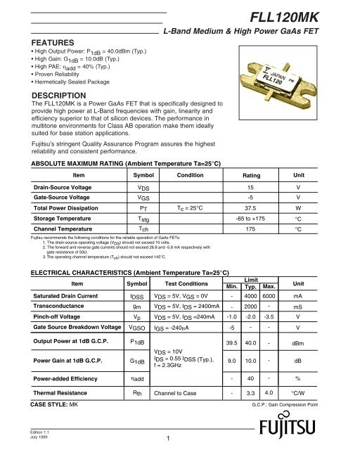
FLL120MK DATASHT(color) - Modelithics, Inc.
FLL120MK DATASHT(color) - Modelithics, Inc.
FLL120MK DATASHT(color) - Modelithics, Inc.

Create successful ePaper yourself
Turn your PDF publications into a flip-book with our unique Google optimized e-Paper software.
FEATURES<br />
• High Output Power: P 1dB = 40.0dBm (Typ.)<br />
• High Gain: G 1dB = 10.0dB (Typ.)<br />
• High PAE: η add = 40% (Typ.)<br />
• Proven Reliability<br />
• Hermetically Sealed Package<br />
<strong>FLL120MK</strong><br />
L-Band Medium & High Power GaAs FET<br />
DESCRIPTION<br />
The <strong>FLL120MK</strong> is a Power GaAs FET that is specifically designed to<br />
provide high power at L-Band frequencies with gain, linearity and<br />
efficiency superior to that of silicon devices. The performance in<br />
multitone environments for Class AB operation make them ideally<br />
suited for base station applications.<br />
Fujitsu’s stringent Quality Assurance Program assures the highest<br />
reliability and consistent performance.<br />
ABSOLUTE MAXIMUM RATING (Ambient Temperature Ta=25°C)<br />
Item<br />
Symbol<br />
Condition<br />
Rating<br />
Unit<br />
Drain-Source Voltage<br />
Gate-Source Voltage<br />
Total Power Dissipation<br />
Storage Temperature<br />
Channel Temperature<br />
VDS<br />
VGS<br />
PT<br />
Tstg<br />
Tch<br />
Tc = 25°C<br />
Fujitsu recommends the following conditions for the reliable operation of GaAs FETs:<br />
1. The drain-source operating voltage (V DS ) should not exceed 10 volts.<br />
2. The forward and reverse gate currents should not exceed 26.8 and -5.8 mA respectively with<br />
gate resistance of 50Ω.<br />
3. The operating channel temperature (T ch ) should not exceed 145°C.<br />
15<br />
-5<br />
37.5<br />
-65 to +175<br />
175<br />
V<br />
V<br />
W<br />
°C<br />
°C<br />
ELECTRICAL CHARACTERISTICS (Ambient Temperature Ta=25°C)<br />
Item<br />
Saturated Drain Current<br />
Transconductance<br />
Pinch-off Voltage<br />
Gate Source Breakdown Voltage<br />
Symbol<br />
IDSS<br />
gm<br />
Vp<br />
VGSO<br />
Test Conditions<br />
VDS = 5V, VGS = 0V<br />
VDS = 5V, IDS = 2400mA<br />
VDS = 5V, IDS =240mA<br />
IGS = -240µA<br />
Min.<br />
-<br />
-<br />
-1.0<br />
-5<br />
Limit<br />
Typ.<br />
4000<br />
2000<br />
-2.0<br />
-<br />
Max.<br />
6000<br />
-<br />
-3.5<br />
-<br />
Unit<br />
mA<br />
mS<br />
V<br />
V<br />
Output Power at 1dB G.C.P.<br />
Power Gain at 1dB G.C.P.<br />
P1dB<br />
G1dB<br />
VDS = 10V<br />
IDS = 0.55 IDSS (Typ.),<br />
f = 2.3GHz<br />
39.5 40.0 -<br />
9.0 10.0 -<br />
dBm<br />
dB<br />
Power-added Efficiency<br />
ηadd<br />
- 40 -<br />
%<br />
Thermal Resistance Rth Channel to Case<br />
- 3.3 4.0 °C/W<br />
CASE STYLE: MK<br />
G.C.P.: Gain Compression Point<br />
Edition 1.1<br />
July 1999<br />
1
<strong>FLL120MK</strong><br />
L-Band Medium & High Power GaAs FET<br />
50<br />
POWER DERATING CURVE<br />
DRAIN CURRENT vs. DRAIN-SOURCE VOLTAGE<br />
Total Power Dissipation (W)<br />
40<br />
30<br />
20<br />
10<br />
Drain Current (mA)<br />
4000<br />
3000<br />
2000<br />
1000<br />
VGS =0V<br />
-0.5V<br />
-1.0V<br />
-1.5V<br />
0 50 100 150 200 0 2 4 6 8 10<br />
Case Temperature (°C)<br />
Drain-Source Voltage (V)<br />
-2.0V<br />
OUTPUT POWER vs. INPUT POWER<br />
42<br />
VDS=10V<br />
IDS ≈ 0.55 IDSS<br />
f = 2.3 GHz<br />
Output Power (dBm)<br />
40<br />
38<br />
36<br />
34<br />
32<br />
P out<br />
η add<br />
60<br />
40<br />
20<br />
ηadd (%)<br />
30<br />
20 22 24 26 28 30 32<br />
0<br />
Input Power (dBm)<br />
2
<strong>FLL120MK</strong><br />
L-Band Medium & High Power GaAs FET<br />
+j10<br />
0<br />
+j50<br />
+j25<br />
4.5<br />
4.0<br />
5.0 GHz<br />
3.5 4.5<br />
4.0<br />
3.0 3.5<br />
2.5 3.0<br />
2.0 2.0<br />
0.5GHz10 25 50Ω<br />
1.0<br />
0.5GHz<br />
5.0 GHz<br />
100<br />
+j100<br />
250<br />
+j250<br />
S 11<br />
S 22<br />
180°<br />
+90°<br />
0.5 GHz<br />
1.5<br />
3.0<br />
4 3 2 1<br />
SCALE FOR |S 21 |<br />
5.0 GHz<br />
1<br />
4.5<br />
4.0<br />
4.5<br />
4.0<br />
2.0 5.0 GHz<br />
0.5GHz<br />
S 21<br />
S 12<br />
0°<br />
-j10<br />
-j25<br />
-j50<br />
-j100<br />
-j250<br />
SCALE FOR |S 12 |<br />
-90°<br />
0.1<br />
0.2<br />
S-PARAMETERS<br />
V DS = 10V, I DS = 2200mA<br />
FREQUENCY S11 S21 S12 S22<br />
(MHZ) MAG ANG MAG ANG MAG ANG MAG ANG<br />
500 .959 -168.4 3.136 95.8 .008 31.0 .824 179.4<br />
1000 .953 -176.0 1.617 94.1 .010 45.7 .813 178.8<br />
1500 .953 -179.6 1.170 93.8 .011 64.3 .810 177.7<br />
2000 .951 177.0 .978 92.3 .014 82.4 .792 176.5<br />
2500 .939 172.6 .927 91.4 .021 89.1 .778 174.0<br />
3000 .914 165.1 .936 88.0 .024 93.2 .739 168.3<br />
3500 .885 152.7 .990 80.6 .033 94.6 .695 158.9<br />
4000 .836 134.0 1.106 67.1 .051 88.1 .633 145.1<br />
4500 .766 107.3 1.239 48.2 .067 77.3 .559 128.0<br />
5000 .690 71.6 1.415 23.9 .103 60.5 .477 107.3<br />
3
<strong>FLL120MK</strong><br />
L-Band Medium & High Power GaAs FET<br />
Case Style "MK"<br />
Metal-Ceramic Hermetic Package<br />
2-R 1.25<br />
(0.049)<br />
1<br />
2<br />
2.5 Min.<br />
(0.098)<br />
0.1<br />
(0.004)<br />
1.0±0.1<br />
(0.039)<br />
2.5 Min.<br />
(0.098)<br />
1.78<br />
(0.073)<br />
14.3±0.2<br />
(0.563)<br />
4.5 Max.<br />
(0.177)<br />
6.3±0.2<br />
(0.25)<br />
4.8<br />
(0.188)<br />
3<br />
17.5±0.2<br />
(0.689)<br />
2.28±0.2<br />
(0.089)<br />
8.9<br />
(0.349)<br />
1. Gate<br />
2. Source (Flange)<br />
3. Drain<br />
Unit: mm(inches)<br />
For further information please contact:<br />
FUJITSU COMPOUND SEMICONDUCTOR, INC.<br />
2355 Zanker Rd.<br />
San Jose, CA 95131-1138, U.S.A.<br />
Phone: (408) 232-9500<br />
FAX: (408) 428-9111<br />
www.fcsi.fujitsu.com<br />
FUJITSU MICROELECTRONICS, LTD.<br />
Compound Semiconductor Division<br />
Network House<br />
Norreys Drive<br />
Maidenhead, Berkshire SL6 4FJ<br />
Phone:+44 (0)1628 504800<br />
FAX:+44 (0)1628 504888<br />
CAUTION<br />
Fujitsu Compound Semiconductor Products contain gallium arsenide<br />
(GaAs) which can be hazardous to the human body and the environment.<br />
For safety, observe the following procedures:<br />
• Do not put these products into the mouth.<br />
• Do not alter the form of this product into a gas, powder, or liquid<br />
through burning, crushing, or chemical processing as these by-products<br />
are dangerous to the human body if inhaled, ingested, or swallowed.<br />
• Observe government laws and company regulations when discarding this<br />
product. This product must be discarded in accordance with methods<br />
specified by applicable hazardous waste procedures.<br />
Fujitsu Limited reserves the right to change products and specifications without notice.<br />
The information does not convey any license under rights of Fujitsu Limited or others.<br />
© 1998 FUJITSU COMPOUND SEMICONDUCTOR, INC.<br />
Printed in U.S.A. FCSI0598M200<br />
4