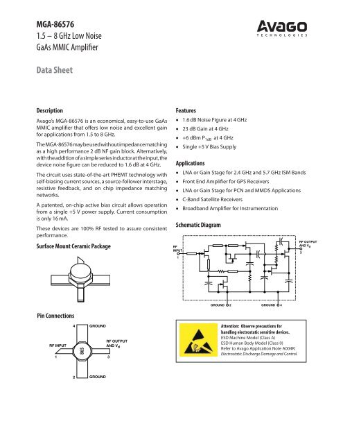
MGA-86576 1.5 – 8 GHz Low Noise GaAs MMIC Amplifier Data Sheet
MGA-86576 1.5 – 8 GHz Low Noise GaAs MMIC Amplifier Data Sheet
MGA-86576 1.5 – 8 GHz Low Noise GaAs MMIC Amplifier Data Sheet

You also want an ePaper? Increase the reach of your titles
YUMPU automatically turns print PDFs into web optimized ePapers that Google loves.
<strong>MGA</strong>-<strong>86576</strong><br />
<strong>1.5</strong> <strong>–</strong> 8 <strong>GHz</strong> <strong>Low</strong> <strong>Noise</strong><br />
<strong>GaAs</strong> <strong>MMIC</strong> <strong>Amplifier</strong><br />
<strong>Data</strong> <strong>Sheet</strong><br />
Description<br />
Avago’s <strong>MGA</strong>-<strong>86576</strong> is an economical, easy-to-use <strong>GaAs</strong><br />
<strong>MMIC</strong> amplifier that offers low noise and excellent gain<br />
for applications from <strong>1.5</strong> to 8 <strong>GHz</strong>.<br />
The<strong>MGA</strong>-<strong>86576</strong>maybeusedwithoutimpedancematching<br />
as a high performance 2 dB NF gain block. Alternatively,<br />
withtheadditionofasimpleseriesinductorattheinput,the<br />
device noise figure can be reduced to 1.6 dB at 4 <strong>GHz</strong>.<br />
The circuit uses state-of-the-art PHEMT technology with<br />
self-biasing current sources, a source-follower interstage,<br />
resistive feedback, and on chip impedance matching<br />
networks.<br />
A patented, on-chip active bias circuit allows operation<br />
from a single +5 V power supply. Current consumption<br />
is only 16 mA.<br />
These devices are 100% RF tested to assure consistent<br />
performance.<br />
Surface Mount Ceramic Package RF<br />
INPUT<br />
Pin Connections <strong>MGA</strong>-<strong>86576</strong> Pkg<br />
RF INPUT<br />
4 GROUND<br />
1 3<br />
2<br />
865<br />
GROUND<br />
<strong>MGA</strong>-<strong>86576</strong> Pin Connection<br />
RF OUTPUT<br />
AND V d<br />
Features<br />
• 1.6 dB <strong>Noise</strong> Figure at 4 <strong>GHz</strong><br />
• 23 dB Gain at 4 <strong>GHz</strong><br />
• +6 dBm P 1dB at 4 <strong>GHz</strong><br />
• Single +5 V Bias Supply<br />
Applications<br />
• LNA or Gain Stage for 2.4 <strong>GHz</strong> and 5.7 <strong>GHz</strong> ISM Bands<br />
• Front End <strong>Amplifier</strong> for GPS Receivers<br />
• LNA or Gain Stage for PCN and MMDS Applications<br />
• C-Band Satellite Receivers<br />
• Broadband <strong>Amplifier</strong> for Instrumentation<br />
Schematic Diagram<br />
1<br />
GROUND<br />
2 GROUND 4<br />
<strong>MGA</strong>-<strong>86576</strong> Schematic<br />
Attention: Observe precautions for<br />
handling electrostatic sensitive devices.<br />
ESD Machine Model (Class A)<br />
ESD Human Body Model (Class 0)<br />
Refer to Avago Application Note A004R:<br />
Electrostatic Discharge Damage and Control.<br />
RF OUTPUT<br />
AND V d<br />
3
Absolute Maximum Ratings<br />
2<br />
Absolute<br />
Symbol Parameter Units Maximum [1]<br />
V d Device Voltage, RF output V 9<br />
to ground<br />
V g Device Voltage, RF input V +0.5<br />
to ground -1.0<br />
P in CW RF Input Power dBm +13<br />
T ch Channel Temperature °C 150<br />
T STG Storage Temperature °C -65 to 150<br />
<strong>MGA</strong>-<strong>86576</strong> Electrical Specifications, T C = 25°C, Z o = 50 Ω, V d = 5 V<br />
Thermal Resistance [2] :<br />
θ ch-c = 110°C/W<br />
Notes:<br />
1. Operation of this device above any one of<br />
these limits may cause permanent damage.<br />
2. T c = 25°C (T c is defined to be the temperature<br />
at the package pins where contact is<br />
made to the circuit board).<br />
Symbol Parameters and Test Conditions Units Min. Typ. Max.<br />
Gp Power Gain (|S 21| 2 ) f = <strong>1.5</strong> <strong>GHz</strong> dB 21.2<br />
f = 2.5 <strong>GHz</strong> 23.7<br />
f = 4.0 <strong>GHz</strong> 20 23.1<br />
f = 6.0 <strong>GHz</strong> 19.3<br />
f = 8.0 <strong>GHz</strong> 15.4<br />
NF 50 50 Ω <strong>Noise</strong> Figure f = <strong>1.5</strong> <strong>GHz</strong> dB 2.2<br />
f = 2.5 <strong>GHz</strong> 1.9<br />
f = 4.0 <strong>GHz</strong> 2.0 2.3<br />
f = 6.0 <strong>GHz</strong> 2.3<br />
f = 8.0 <strong>GHz</strong> 2.5<br />
NF o Optimum <strong>Noise</strong> Figure f = <strong>1.5</strong> <strong>GHz</strong> dB 1.6<br />
(Input tuned for lowest noise f = 2.5 <strong>GHz</strong> <strong>1.5</strong><br />
figure) f = 4.0 <strong>GHz</strong> 1.6<br />
f = 6.0 <strong>GHz</strong> 1.8<br />
f = 8.0 <strong>GHz</strong> 2.1<br />
P 1dB Output Power at 1 dB Gain f = <strong>1.5</strong> <strong>GHz</strong> dBm 6.4<br />
Compression f = 2.5 <strong>GHz</strong> 7.0<br />
f = 4.0 <strong>GHz</strong> 6.3<br />
f = 6.0 <strong>GHz</strong> 4.3<br />
f = 8.0 <strong>GHz</strong> 3.8<br />
IP 3 Third Order Intercept Point f = 4.0 <strong>GHz</strong> dBm 16.0<br />
VSWR Input VSWR f = <strong>1.5</strong> <strong>GHz</strong> 3.6:1<br />
f = 2.5 <strong>GHz</strong> 3.3:1<br />
f = 4.0 <strong>GHz</strong> 2.2:1 3.6:1<br />
f = 6.0 <strong>GHz</strong> 1.4:1<br />
f = 8.0 <strong>GHz</strong> 1.2:1<br />
Output VSWR f = <strong>1.5</strong> <strong>GHz</strong> 2.5:1<br />
f = 2.5 <strong>GHz</strong> 2.1:1<br />
f = 4.0 <strong>GHz</strong> 1.7:1<br />
f = 6.0 <strong>GHz</strong> 1.4:1<br />
f = 8.0 <strong>GHz</strong> 1.3:1<br />
I d Device Current mA 9 16 22
<strong>MGA</strong>-<strong>86576</strong> Typical Performance, T C = 25°C, Z o = 50 Ω, V d = 5 V<br />
GAIN (dB)<br />
Figure 1. Power Gain vs. Frequency at Three Temperatures.<br />
P 1dB (dBm)<br />
3<br />
30.0<br />
25.0<br />
20.0<br />
15.0<br />
10.0<br />
5.0<br />
1<br />
10.0<br />
8.0<br />
6.0<br />
4.0<br />
2.0<br />
0<br />
1<br />
-40°C<br />
+25°C<br />
+50°C<br />
2 3 4 5 6 7 8 9 10<br />
-40°C<br />
+25°C<br />
+50°C<br />
FREQUENCY (<strong>GHz</strong>)<br />
<strong>MGA</strong>-<strong>86576</strong> fig 1<br />
2 3 4 5 6 7 8 9 10<br />
FREQUENCY (<strong>GHz</strong>)<br />
NF (dB)<br />
3.5<br />
3<br />
2.5<br />
2<br />
<strong>1.5</strong><br />
1<br />
1<br />
+50°C<br />
+25°C<br />
-40°C<br />
2 3 4 5 6 7 8 9 10<br />
FREQUENCY (<strong>GHz</strong>)<br />
Figure 2. 50 Ω <strong>Noise</strong> Figure vs. Frequency at Three<br />
Temperatures.<br />
<strong>MGA</strong>-<strong>86576</strong> fig 2<br />
NF (dB)<br />
3.5<br />
3<br />
2.5<br />
2<br />
<strong>1.5</strong><br />
1<br />
1<br />
2 3 4 5 6 7 8 9 10<br />
FREQUENCY (<strong>GHz</strong>)<br />
Figure 3. Matched <strong>Noise</strong> Figure vs. Frequency.<br />
<strong>MGA</strong>-<strong>86576</strong> fig 3<br />
Figure 4. P 1dB vs. Frequency at Three Temperatures. Figure 5. Input and Output VSWR vs. Frequency. Figure 6. Gain, NF 50, and P 1dB vs. Temperature at 4<br />
<strong>GHz</strong>.<br />
<strong>MGA</strong>-<strong>86576</strong> fig 4<br />
VSWR<br />
4.0<br />
3.5<br />
3.0<br />
2.5<br />
2.0<br />
<strong>1.5</strong><br />
1.0<br />
1<br />
INPUT<br />
OUTPUT<br />
2 3 4 5 6 7 8 9 10<br />
FREQUENCY (<strong>GHz</strong>)<br />
<strong>MGA</strong>-<strong>86576</strong> fig 5<br />
<strong>MGA</strong>-<strong>86576</strong> Typical Scattering Parameters [3] , T C = 25°C, Z o = 50 Ω, V d = 5 V<br />
GAIN AND NF (dB)<br />
25<br />
20<br />
15<br />
10<br />
5<br />
0<br />
-40<br />
POWER GAIN<br />
P 1dB<br />
NOISE FIGURE<br />
0<br />
-30 -20 -10 0 25 50<br />
TEMPERATURE °C<br />
<strong>MGA</strong>-<strong>86576</strong> fig 6<br />
Freq. S 11 S 21 S 12 S 22<br />
<strong>GHz</strong><br />
Mag Ang dB Mag Ang dB Mag Ang Mag Ang<br />
0.5 0.57 -21 15.5 5.99 46 -46.5 0.005 -15 0.62 -35<br />
1.0 0.55 -30 19.8 9.72 17 -51.3 0.003 11 0.49 -47<br />
<strong>1.5</strong> 0.54 -44 21.7 12.15 -7 -51.2 0.003 58 0.43 -57<br />
2.0 0.52 -59 22.8 13.84 -31 -47.0 0.004 85 0.39 -68<br />
2.5 0.48 -77 23.5 14.98 -54 -43.0 0.007 96 0.36 -79<br />
3.0 0.43 -96 23.8 15.56 -77 -39.7 0.010 100 0.33 -92<br />
3.5 0.37 -116 23.7 15.28 -100 -37.0 0.014 99 0.29 -105<br />
4.0 0.30 -137 23.2 14.49 -122 -35.0 0.018 95 0.25 -118<br />
4.5 0.24 -159 22.4 13.18 -142 -33.2 0.022 92 0.21 -130<br />
5.0 0.19 178 2<strong>1.5</strong> 11.82 -160 -31.9 0.026 89 0.19 -139<br />
5.5 0.14 151 20.5 10.54 -177 -30.6 0.030 85 0.14 -151<br />
6.0 0.12 129 19.2 9.14 166 -29.6 0.033 81 0.17 -151<br />
6.5 0.10 111 18.1 8.08 156 -28.7 0.037 82 0.14 -116<br />
7.0 0.08 91 17.5 7.48 142 -27.4 0.042 76 0.08 -158<br />
7.5 0.08 75 16.4 6.64 129 -26.6 0.047 72 0.11 -153<br />
8.0 0.07 64 15.5 5.99 118 -25.8 0.051 69 0.09 -151<br />
8.5 0.06 48 14.7 5.45 107 -25.0 0.056 65 0.09 -146<br />
9.0 0.04 31 14.0 5.03 96 -24.2 0.062 62 0.09 -140<br />
9.5 0.02 18 13.4 4.66 86 -23.4 0.068 58 0.11 -143<br />
10.0 0.01 93 12.7 4.33 76 -22.6 0.074 53 0.11 -154<br />
+10<br />
+5<br />
P 1dB (dBm)
<strong>MGA</strong>-<strong>86576</strong> Typical <strong>Noise</strong> Parameters [3] ,<br />
T C = 25°C, Z o = 50 Ω, V d = 5 V<br />
Frequency NF o Γopt<br />
4<br />
<strong>GHz</strong> dB Mag. Ang. R N/50 Ω<br />
1.0 2.1 0.56 27 0.43<br />
<strong>1.5</strong> 1.6 0.54 31 0.40<br />
2.5 <strong>1.5</strong> 0.47 40 0.36<br />
4.0 1.6 0.38 54 0.32<br />
6.0 1.8 0.28 77 0.28<br />
8.0 2.1 0.22 107 0.25<br />
[3] Reference plane taken at point where leads meet body of package.<br />
<strong>MGA</strong>-<strong>86576</strong> Applications Information<br />
Introduction<br />
The <strong>MGA</strong>-<strong>86576</strong> is a high gain, broad band, low noise<br />
amplifier. The use of plated through holes or an equivalent<br />
minimal inductance grounding technique placed<br />
precisely under each ground lead at the device is highly<br />
recom-mended. A minimum of two plated through holes<br />
undereachgroundleadispreferredwithfourbeinghighly<br />
suggested. A long ground path to pins 2 and 4 will add<br />
additionalinductancewhichcancausegainpeakinginthe<br />
2 to 4 <strong>GHz</strong> frequency range.This can also be accompanied<br />
by a decrease in stability. A suggested layout is shown in<br />
Figure 7. The circuit is designed for use on 0.031 inch thick<br />
FR-4/G-10 epoxy glass dielectric material.<br />
Printed circuit board thickness is also a major consideration.<br />
Thicker printed circuit boards dictate longer<br />
plated through holes which provide greater undesired<br />
inductance. The parasitic inductance associated with a<br />
pair of plated through holes passing through 0.031 inch<br />
thick printed circuit board is approximately 0.1 nH, while<br />
the inductance of a pair of plated through holes passing<br />
through0.062inchthickboardisabout0.2 nH.Avagodoes<br />
not recommend using the <strong>MGA</strong>-<strong>86576</strong> <strong>MMIC</strong> on boards<br />
thicker than 0.040 inch.<br />
Figure 7. Layout for <strong>MGA</strong>-<strong>86576</strong> Demonstration <strong>Amplifier</strong>.<br />
PCB dimensions are 1.18 inches wide by 1.30 inches high.<br />
The effects of inductance associated with the board<br />
material are easily analyzed and very predict-able. As a<br />
minimum, the circuit simulation should consist of the data<br />
sheetS-Parametersandanadditionalcircuitfiledescribing<br />
the plated through holes and any additional inductance<br />
associated with lead length between the device and the<br />
start of the plated through hole. To obtain a complete<br />
analysis of the entire amplifier circuit, the effects of the<br />
input and output microstriplines and bias decoupling<br />
circuits should be incorporated into the circuit file.<br />
Device Connections V d and RF Output (Pin 3)<br />
RF and DC connections are shown in Figure 8. DC power<br />
is provided to the <strong>MMIC</strong> through the same pin used to<br />
obtain RF output. A 50 Ω microstripline is used to connect<br />
the device to the following stage or output connector.<br />
A bias decoupling network is used to feed in V dd while<br />
simultaneously providing a DC block to the RF signal. The<br />
bias decoupling network shown in Figure 8, consisting of<br />
resistor R1, a short length of high impedance microstripline,<br />
and bypass capacitor C1, provides the best overall<br />
performance in the 2 to 8 <strong>GHz</strong> frequency range.<br />
27 pF<br />
100-1000 pF<br />
C1<br />
V dd<br />
HIGH Z<br />
10-100 Ω<br />
50 Ω 50 Ω 50 Ω 50 Ω<br />
2<br />
<strong>MGA</strong>-<strong>86576</strong> fig 8<br />
Figure 8. Demonstration <strong>Amplifier</strong> Schematic.<br />
L1<br />
1<br />
4<br />
R1<br />
3<br />
27 pF
The use of lumped inductors is not desired since they<br />
tendto radiateandcauseundesiredfeedback.Movingthe<br />
bypass capacitor, C1, down the microstripline towards the<br />
V dd terminal, as shown in Figure 9, will improve the gain<br />
below 2 <strong>GHz</strong> by trading off some high end gain. A minimum<br />
value of 10 Ω for R1 is recommended to de-Q the<br />
bias decoupling network, although 100 Ω will provide the<br />
highest circuit gain over the entire <strong>1.5</strong> to 8 <strong>GHz</strong> frequency<br />
range. V dd will have to be increased accordingly for higher<br />
values of R1. For operation in the 2 to 6 <strong>GHz</strong> frequency<br />
range, a 10 pF capacitor may be used for DC blocking on<br />
the output microstripline. A larger value such as 27 pF is<br />
more appropriate for operation at <strong>1.5</strong> <strong>GHz</strong>.<br />
Figure 9. Complete <strong>MGA</strong>-<strong>86576</strong> Demonstration <strong>Amplifier</strong>.<br />
Ground (Pins 2 and 4)<br />
Groundpinsshouldattachdirectlytothebacksideground<br />
plane by the shortest distance possible using the design<br />
hints suggested in the earlier section. Liberal use of plated<br />
through vias is recommended.<br />
RF Input (Pin 1)<br />
A 50 Ω microstripline can be used to feed RF to the device.<br />
A blocking capacitor in the 10 pF range will provide<br />
a suitable DC block in the 2 to 6 <strong>GHz</strong> frequency range.<br />
Although there is no voltage present at pin 1, it is highly<br />
suggestedthataDCblockingcapacitorbeusedtoprevent<br />
accidental application of a voltage from a previous amplifierstage.With<br />
nofurtherinput matching, the <strong>MGA</strong>-<strong>86576</strong><br />
is capable of noise figures as low as 2 dB in the 2 to 6 <strong>GHz</strong><br />
frequency range. Since Γ o is not 50 Ω, it is possible to design<br />
and implement a very simple matching network in<br />
order to improve noise figure and input return loss over a<br />
narrow frequency range. The circuit board layout shown<br />
in Figure 7 provides an option for tuning for a low noise<br />
match anywhere in the <strong>1.5</strong> to 4 <strong>GHz</strong> frequency range. For<br />
optimumnoisefigureperformanceinthe4 <strong>GHz</strong>frequency<br />
range, L1 can be a 0.007 inch diameter wire 0.080 inches<br />
in length as shown in Figure 9. Alternatively, L1 can be<br />
replaced by a 0.020 inch wide microstripline whose length<br />
can be adjusted for minimum noise figure in the <strong>1.5</strong> to 4<br />
<strong>GHz</strong> frequency range.<br />
5<br />
Table 1 provides the approximate inductor length for<br />
minimum noise figure at a given frequency for the circuit<br />
board shown in Figure 7.<br />
Table 1. L1 Length vs. Frequency for Optimum <strong>Noise</strong> Figure.<br />
Frequency Length<br />
<strong>GHz</strong> Inches<br />
<strong>1.5</strong> 0.70<br />
1.8 0.60<br />
2.1 0.50<br />
2.4 0.40<br />
2.5 0.30<br />
3.0 0.20<br />
3.7 0.10<br />
4.0 0.05<br />
7 Volt Bias for Operation at Higher Temperatures<br />
The <strong>MGA</strong>-<strong>86576</strong> was designed primarily for 5 volt operation<br />
over the -25 to +50°C temperature range. For<br />
applications requiring use to +85°C, a 7 volt bias supply<br />
is recommended to minimize changes in gain and noise<br />
figure at elevated temperature. Figure 10 shows typical<br />
gain, noise figure, and output power performance over<br />
temperature at 4 <strong>GHz</strong> with 7 volts applied. With a 7 volt<br />
bias supply, output power is increased approximately <strong>1.5</strong><br />
dB. Other parameters are relatively unchanged from 5 volt<br />
data. S-parameter and noise parameter data for 7 volts are<br />
available upon request from Avago.<br />
dB OR dE<br />
25<br />
20<br />
15<br />
10<br />
5<br />
POWER GAIN<br />
P 1dB<br />
NOISE FIGURE<br />
0<br />
-40 -30 -20 -10 0 25 50<br />
TEMPERATURE °C<br />
<strong>MGA</strong>-<strong>86576</strong> fig 10<br />
85 125<br />
Figure 10. Gain, NF50, and P1dB vs. Temperature at 4<br />
<strong>GHz</strong> with 7 Volt Bias Supply.
Printed Circuit Board Materials<br />
Most commercial applications dictate the need to use<br />
inexpensive epoxy glass materials such as FR-4 or G-10.<br />
Unfortunatelythelossesofthistypeofmaterialcanbecome<br />
excessive above 2 <strong>GHz</strong>. As an example, a 0.5 inch long<br />
50 Ω microstripline etched on FR-4 along with a blocking<br />
capacitor has a measured loss of 0.35 dB at 4 <strong>GHz</strong>.The 0.35<br />
dB loss adds directly to the noise figure of the <strong>MGA</strong>-<strong>86576</strong>.<br />
The use of a low loss PTFE based dielectric material will<br />
preserve the inherent low noise of the <strong>MGA</strong>-<strong>86576</strong>.<br />
Part Number Ordering Information<br />
No. of<br />
Part Number Devices Container<br />
<strong>MGA</strong>-<strong>86576</strong>-TR1 1000 7" Reel<br />
<strong>MGA</strong>-<strong>86576</strong>-STRG 100 Strips<br />
Package Dimensions<br />
76 Package<br />
1.22<br />
(0.048)<br />
.51<br />
(0.20)<br />
.53<br />
(0.021)<br />
For product information and a complete list of distributors, please go to our web site: www.avagotech.com<br />
vago, Avago Technologies, and the A logo are trademarks of Avago Technologies Limited in the United States and other countries.<br />
<strong>Data</strong> subject to change. Copyright © 2005-2008 Avago Technologies Limited. All rights reserved. Obsoletes 5989-4658EN<br />
AV02-0608EN - April 29, 2008<br />
1.02<br />
(0.040)<br />
1.78<br />
(0.070)<br />
5.28<br />
(0.208)<br />
<strong>MGA</strong>-<strong>86576</strong> Pkg Dimensions<br />
0.10<br />
(0.004)<br />
TYPICAL DIMENSIONS ARE IN MILLIMETERS (INCHES).