Xilinx Spartan and SpartanXL Families (XCS00) FPGA Families data ...
Xilinx Spartan and SpartanXL Families (XCS00) FPGA Families data ...
Xilinx Spartan and SpartanXL Families (XCS00) FPGA Families data ...

You also want an ePaper? Increase the reach of your titles
YUMPU automatically turns print PDFs into web optimized ePapers that Google loves.
marc<br />
0<br />
R<br />
<strong>Spartan</strong> <strong>and</strong> <strong>Spartan</strong>XL <strong>Families</strong><br />
Field Programmable Gate Arrays<br />
January 6, 1999 (Version 1.4) 0 4 Preliminary Product Specification<br />
Introduction<br />
The <strong>Spartan</strong> TM Series is the first high-volume production<br />
<strong>FPGA</strong> solution to deliver all the key requirements for ASIC<br />
replacement up to 40,000 gates. These requirements<br />
include high performance, on-chip RAM, Core Solutions<br />
<strong>and</strong> prices that, in high volume, approach <strong>and</strong> in many<br />
cases are equivalent to mask programmed ASIC devices.<br />
The <strong>Spartan</strong> Series is the result of more than thirteen years<br />
of <strong>FPGA</strong> design experience <strong>and</strong> feedback from thous<strong>and</strong>s<br />
of customers. By streamlining the <strong>Spartan</strong> feature set,<br />
leveraging advanced hybrid process technologies <strong>and</strong><br />
focusing on total cost management, the <strong>Spartan</strong> Series<br />
delivers the key features required by ASIC <strong>and</strong> other high<br />
volume logic users while avoiding the initial cost, long<br />
development cycles <strong>and</strong> inherent risk of conventional<br />
ASICs. The <strong>Spartan</strong> Series currently has 10 members, as<br />
shown in Table 1.<br />
<strong>Spartan</strong> Series Features<br />
Note: The <strong>Spartan</strong> Series devices described in this <strong>data</strong><br />
sheet include the 5 V <strong>Spartan</strong> family of devices <strong>and</strong> the<br />
3.3 V <strong>Spartan</strong>XL family of devices.<br />
• Next generation ASIC replacement technology<br />
- First ASIC replacement <strong>FPGA</strong> for high-volume<br />
production with on-chip RAM<br />
- Advanced process technology<br />
- Density up to 1862 logic cells or 40,000 system<br />
gates<br />
- Streamlined feature set based on XC4000<br />
architecture<br />
- System performance beyond 80 MHz<br />
- Broad set of AllianceCORE <strong>and</strong> LogiCORE <br />
pre-defined solutions available<br />
- Unlimited reprogrammability<br />
- Low cost<br />
• System level features<br />
- Available in both 5.0 Volt <strong>and</strong> 3.3 Volt versions<br />
- On-chip SelectRAM TM memory<br />
- Fully PCI compliant<br />
- Low power segmented routing architecture<br />
- Full readback capability for program verification <strong>and</strong><br />
internal node observability<br />
- Dedicated high-speed carry logic<br />
- Internal 3-state bus capability<br />
- 8 global low-skew clock or signal networks<br />
- IEEE 1149.1-compatible boundary scan logic<br />
• Versatile I/O <strong>and</strong> packaging<br />
- Low cost plastic packages available in all densities<br />
- Footprint compatibility in common packages<br />
- Individually programmable output slew-rate control<br />
maximizes performance <strong>and</strong> reduces noise<br />
- Zero input register hold time simplifies system timing<br />
• Fully supported by powerful <strong>Xilinx</strong> development system<br />
- Foundation series: Integrated, shrink-wrap software<br />
- Alliance series: Over 100 PC <strong>and</strong> workstation 3 RD<br />
party development systems supported<br />
- Fully automatic mapping, placement <strong>and</strong> routing<br />
- Interactive design editor for design optimization<br />
Additional <strong>Spartan</strong>XL Features<br />
• 3.3V supply for low power with 5V tolerant I/Os<br />
• Power down input<br />
• Higher performance<br />
• Faster carry logic<br />
• More flexible high-speed clock network<br />
• Latch capability in Configurable Logic Blocks<br />
• Input fast capture latch<br />
• Optional mux or 2-input function generator on outputs<br />
• 12 mA or 24 mA output drive<br />
• 5V/3.3V PCI compliant<br />
• Enhanced Boundary Scan<br />
• Express Mode configuration<br />
4<br />
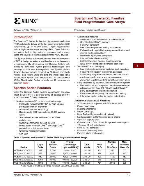
Table 1: <strong>Spartan</strong> <strong>and</strong> <strong>Spartan</strong>XL Series Field Programmable Gate Arrays<br />
Device<br />
Logic<br />
Cells<br />
Max<br />
System<br />
Gates<br />
Typical<br />
Gate Range<br />
(Logic <strong>and</strong> RAM)*<br />
CLB<br />
Matrix<br />
Total<br />
CLBs<br />
Number<br />
of<br />
Flip-Flops<br />
Max.<br />
Available<br />
User I/O<br />
XCS05 & XCS05XL 238 5,000 2,000 - 5,000 10 x 10 100 360 77<br />
XCS10 & XCS10XL 466 10,000 3,000 - 10,000 14 x 14 196 616 112<br />
XCS20 & XCS20XL 950 20,000 7,000 - 20,000 20 x 20 400 1,120 160<br />
XCS30 & XCS30XL 1368 30,000 10,000 - 30,000 24 x 24 576 1,536 192<br />
XCS40 & XCS40XL 1862 40,000 13,000 - 40,000 28 x 28 784 2,016 205<br />
*Max values of Typical Gate Range include 20-30% of CLBs used as RAM.<br />
January 6, 1999 (Version 1.4) 4-3
R<br />
<strong>Spartan</strong> <strong>and</strong> <strong>Spartan</strong>XL <strong>Families</strong> Field Programmable Gate Arrays<br />
General Overview<br />
<strong>Spartan</strong> Series <strong>FPGA</strong>s are implemented with a regular,<br />
flexible, programmable architecture of Configurable Logic<br />
Blocks (CLBs), interconnected by a powerful hierarchy of<br />
versatile routing resources (routing channels), <strong>and</strong> surrounded<br />
by a perimeter of programmable Input/Output<br />
Blocks (IOBs), as seen in Figure 1. They have generous<br />
routing resources to accommodate the most complex interconnect<br />
patterns.<br />
The devices are customized by loading configuration <strong>data</strong><br />
into internal static memory cells. Re-programming is possible<br />
an unlimited number of times. The values stored in<br />
these memory cells determine the logic functions <strong>and</strong> interconnections<br />
implemented in the <strong>FPGA</strong>. The <strong>FPGA</strong> can<br />
either actively read its configuration <strong>data</strong> from an external<br />
serial PROM (Master Serial mode), or the configuration<br />
<strong>data</strong> can be written into the <strong>FPGA</strong> from an external device<br />
(Slave Serial mode).<br />
<strong>Spartan</strong> <strong>FPGA</strong>s can be used where hardware must be<br />
adapted to different user applications. <strong>FPGA</strong>s are ideal for<br />
shortening design <strong>and</strong> development cycles, <strong>and</strong> also offer a<br />
cost-effective solution for production rates well beyond<br />
50,000 systems per month.<br />
<strong>Spartan</strong> Series devices achieve high-performance,<br />
low-cost operation through the use of an advanced architecture<br />
<strong>and</strong> semiconductor technology. <strong>Spartan</strong> <strong>and</strong> <strong>Spartan</strong>XL<br />
devices provide system clock rates exceeding<br />
80 MHz <strong>and</strong> internal performance in excess of 150 MHz.<br />
In contrast to other <strong>FPGA</strong> devices, <strong>Spartan</strong> <strong>FPGA</strong>s offer<br />
the most cost-effective solution while maintaining leading-edge<br />
performance. In addition to the conventional benefit<br />
of high volume programmable logic solutions <strong>Spartan</strong><br />
<strong>FPGA</strong>s also offer on-chip edge-triggered single-port <strong>and</strong><br />
dual-port RAM, clock enables on all flip-flops, fast carry<br />
logic, <strong>and</strong> many other features.<br />
The <strong>Spartan</strong> Series leverages the highly successful<br />
XC4000 architecture with many of that family’s features <strong>and</strong><br />
benefits. Technology advancements have been derived<br />
from the XC4000XLA <strong>and</strong> XC4000XV process developments.<br />
B-<br />
SCAN<br />
IOB<br />
IOB<br />
IOB<br />
IOB<br />
IOB<br />
IOB<br />
IOB<br />
IOB<br />
OSC<br />
IOB<br />
IOB<br />
CLB CLB CLB CLB<br />
IOB<br />
IOB<br />
IOB<br />
IOB<br />
IOB<br />
IOB<br />
CLB CLB<br />
CLB CLB<br />
Routing Channels<br />
CLB CLB CLB CLB<br />
IOB<br />
IOB<br />
IOB<br />
IOB<br />
IOB<br />
IOB<br />
CLB CLB<br />
CLB CLB<br />
IOB<br />
IOB<br />
RDBK<br />
IOB<br />
IOB<br />
IOB<br />
IOB<br />
IOB<br />
IOB<br />
VersaRing Routing Channel<br />
IOB<br />
IOB<br />
START<br />
-UP<br />
Rev 2.0<br />
Figure 1: Basic <strong>FPGA</strong> Block Diagram<br />
4-4 January 6, 1999 (Version 1.4)
R<br />
<strong>Spartan</strong> <strong>and</strong> <strong>Spartan</strong>XL <strong>Families</strong> Field Programmable Gate Arrays<br />
Logic Functional Description<br />
The <strong>Spartan</strong> Series uses a st<strong>and</strong>ard <strong>FPGA</strong> structure as<br />
shown in Figure 1 on page 4. The <strong>FPGA</strong> consists of an<br />
array of configurable logic blocks (CLBs) placed in a matrix<br />
of routing channels. The input <strong>and</strong> output of signals is<br />
achieved through a set of input/output blocks (IOBs) forming<br />
a ring around the CLBs <strong>and</strong> routing channels.<br />
• CLBs provide the functional elements for implementing<br />
the user’s logic.<br />
• IOBs provide the interface between the package pins<br />
<strong>and</strong> internal signal lines.<br />
• Routing channels provide paths to interconnect the<br />
inputs <strong>and</strong> outputs of the CLBs <strong>and</strong> IOBs.<br />
The functionality of each circuit block is customized during<br />
configuration by programming internal static memory cells.<br />
The values stored in these memory cells determine the<br />
logic functions <strong>and</strong> interconnections implemented in the<br />
<strong>FPGA</strong>.<br />
Configurable Logic Blocks (CLBs)<br />
The CLBs are used to implement most of the logic in an<br />
<strong>FPGA</strong>. The principal CLB elements are shown in the simplified<br />
block diagram in Figure 2. There are three look-up<br />
tables (LUT) which are used as logic function generators,<br />
two flip-flops <strong>and</strong> two groups of signal steering multiplexers.<br />
There are also some more advanced features provided by<br />
the CLB which will be covered in the “Advanced Features<br />
Description” on page 15.<br />
Function Generators<br />
Two 16x1 memory look-up tables (F-LUT <strong>and</strong> G-LUT) are<br />
used to implement 4-input function generators, each offering<br />
unrestricted logic implementation of any Boolean function<br />
of up to four independent input signals (F1 to F4 or G1<br />
to G4). Using memory look-up tables the propagation delay<br />
is independent of the function implemented.<br />
A third 3-input function generator (H-LUT) can implement<br />
any Boolean function of its three inputs. Two of these inputs<br />
are controlled by programmable multiplexers (see box “A”<br />
of Figure 2). These inputs can come from the F-LUT or<br />
G-LUT outputs or from CLB inputs. The third input always<br />
comes from a CLB input. The CLB can, therefore, implement<br />
certain functions of up to nine inputs, like parity<br />
checking. The three LUTs in the CLB can also be combined<br />
to do any arbitrarily defined Boolean function of five inputs.<br />
4<br />
G-LUT<br />
B<br />
G4<br />
G3<br />
G2<br />
G1<br />
G4<br />
Logic<br />
G3 Function<br />
of G<br />
G2 G1-G4<br />
G1<br />
H-LUT<br />
SR<br />
D<br />
CK<br />
EC<br />
Q<br />
YQ<br />
SR<br />
H1<br />
DIN<br />
G<br />
Logic<br />
Function<br />
H1 of H<br />
F,G,H1<br />
F<br />
Y<br />
F4<br />
F3<br />
F2<br />
F1<br />
F4<br />
Logic<br />
F3 Function<br />
of F<br />
F2 F1-F4<br />
F1<br />
A<br />
SR<br />
D<br />
CK<br />
EC<br />
Q<br />
XQ<br />
K<br />
F-LUT<br />
Multiplexer Controlled<br />
by Configuration Program<br />
X<br />
EC<br />
Figure 2: <strong>Spartan</strong> Simplified CLB Logic Diagram (some features not shown)<br />
Rev 1.0<br />
January 6, 1999 (Version 1.4) 4-5
R<br />
<strong>Spartan</strong> <strong>and</strong> <strong>Spartan</strong>XL <strong>Families</strong> Field Programmable Gate Arrays<br />
A CLB can implement any of the following functions:<br />
• Any function of up to four variables, plus any second<br />
function of up to four unrelated variables, plus any third<br />
function of up to three unrelated variables 1<br />
• Any single function of five variables<br />
• Any function of four variables together with some<br />
functions of six variables<br />
• Some functions of up to nine variables.<br />
SR<br />
GND<br />
GSR<br />
Implementing wide functions in a single block reduces both<br />
the number of blocks required <strong>and</strong> the delay in the signal<br />
path, achieving both increased capacity <strong>and</strong> speed.<br />
D<br />
D<br />
SD<br />
Q<br />
Q<br />
The versatility of the CLB function generators significantly<br />
improves system speed. In addition, the design-software<br />
tools can deal with each function generator independently.<br />
This flexibility improves cell usage.<br />
Flip-Flops<br />
Each CLB contains two flip-flops that can be used to register<br />
(store) the function generator outputs. The flip-flops <strong>and</strong><br />
function generators can also be used independently (see<br />
Figure 2 on page 5). The CLB input DIN can be used as a<br />
direct input to either of the two flip-flops. H1 can also drive<br />
either flip-flop via the H-LUT with a slight additional delay.<br />
The two flip-flops have common clock (CK), clock enable<br />
(EC) <strong>and</strong> set/reset (SR) inputs. Internally both flip-flops are<br />
also controlled by a global initialization signal (GSR) which<br />
is described in detail in “Global Signals: GSR <strong>and</strong> GTS” on<br />
page 21.<br />
Latches (<strong>Spartan</strong>XL only)<br />
The <strong>Spartan</strong>XL CLB storage elements can also be configured<br />
as latches. The two latches have common clock (K)<br />
<strong>and</strong> clock enable (EC) inputs. Functionality of the storage<br />
element is described in Table 2.<br />
Table 2: CLB Storage Element Functionality<br />
Mode CK EC SR D Q<br />
Power-Up or<br />
GSR<br />
X X X X SR<br />
Flip-Flop<br />
Operation<br />
X X 1 X SR<br />
__/ 1* 0* D D<br />
0 X 0* X Q<br />
Latch Operation 1 1* 0* X Q<br />
(<strong>Spartan</strong>XL) 0 1* 0* D D<br />
Both X 0 0* X Q<br />
Legend:<br />
X<br />
__/<br />
SR<br />
0*<br />
1*<br />
Don’t care<br />
Rising edge (clock not inverted)<br />
Set or Reset value. Reset is default.<br />
Input is Low or unconnected (default value)<br />
Input is High or unconnected (default value)<br />
CK<br />
EC<br />
Vcc<br />
Figure 3: CLB Flip-Flop Functional Block Diagram<br />
Clock Input<br />
Each flip-flop can be triggered on either the rising or falling<br />
clock edge. The CLB clock line is shared by both flip-flops.<br />
However, the clock is individually invertible for each flip-flop<br />
(see CK path in Figure 3). Any inverter placed on the clock<br />
line in the design is automatically absorbed into the CLB.<br />
Clock Enable<br />
The clock enable line (EC) is active High. The EC line is<br />
shared by both flip-flops in a CLB. If either one is left disconnected,<br />
the clock enable for that flip-flop defaults to the<br />
active state. EC is not invertible within the CLB. The clock<br />
enable is synchronous to the clock <strong>and</strong> must satisfy the<br />
setup <strong>and</strong> hold timing specified for the device.<br />
Set/Reset<br />
The set/reset line (SR) is an asynchronous active High control<br />
of the flip-flop. SR can be configured as either set or<br />
reset at each flip-flop. This configuration option determines<br />
the state in which each flip-flop becomes operational after<br />
configuration. It also determines the effect of a GSR pulse<br />
during normal operation, <strong>and</strong> the effect of a pulse on the<br />
SR line of the CLB. The SR line is shared by both flip-flops.<br />
If SR is not specified for a flip-flop the set/reset for that<br />
flip-flop defaults to the inactive state. SR is not invertible<br />
within the CLB.<br />
RD<br />
Rev 1.1<br />
Multiplexer Controlled<br />
by Configuration Program<br />
1. When three separate functions are generated, one of the function outputs must be captured in a flip-flop internal to the CLB. Only two<br />
unregistered function generator outputs are available from the CLB.<br />
4-6 January 6, 1999 (Version 1.4)
R<br />
<strong>Spartan</strong> <strong>and</strong> <strong>Spartan</strong>XL <strong>Families</strong> Field Programmable Gate Arrays<br />
CLB Signal Flow Control<br />
In addition to the H-LUT input control multiplexers (shown<br />
in box “A” of Figure 2 on page 5) there are signal flow control<br />
multiplexers (shown in box “B” of Figure 2) which select<br />
the signals which drive the flip-flop inputs <strong>and</strong> the combinatorial<br />
CLB outputs (X <strong>and</strong> Y).<br />
Each flip-flop input is driven from a 4:1 multiplexer which<br />
selects among the three LUT outputs <strong>and</strong> DIN as the <strong>data</strong><br />
source.<br />
Each combinatorial output is driven from a 2:1 multiplexer<br />
which selects between two of the LUT outputs. The X output<br />
can be driven from the F-LUT or H-LUT, the Y output<br />
from G-LUT or H-LUT.<br />
Control Signals<br />
There are four signal control multiplexers on the input of the<br />
CLB. These multiplexers allow the internal CLB control signals<br />
(H1, DIN, SR, <strong>and</strong> EC in Figure 2 <strong>and</strong> Figure 4) to be<br />
driven from any of the four general control inputs (C1 - C4<br />
in Figure 4) into the CLB. Any of these inputs can drive any<br />
of the four internal control signals.<br />
The four internal control signals are:<br />
• EC - Enable Clock<br />
• SR - Asynchronous Set/Reset or H function generator<br />
Input 0<br />
• DIN - Direct In or H function generator Input 2<br />
• H1 - H function generator Input 1.<br />
Input/Output Blocks (IOBs)<br />
User-configurable input/output blocks (IOBs) provide the<br />
interface between external package pins <strong>and</strong> the internal<br />
logic. Each IOB controls one package pin <strong>and</strong> can be configured<br />
for input, output, or bidirectional signals. Figure 5 on<br />
page 8 shows a simplified functional block diagram of the<br />
<strong>Spartan</strong> IOB.<br />
IOB Input Signal Path<br />
The input signal to the IOB can be configured to either go<br />
directly to the routing channels (via I1 <strong>and</strong> I2 in Figure 5) or<br />
to the input register. The input register can be programmed<br />
as either an edge-triggered flip-flop or a level-sensitive<br />
latch. The functionality of this register is shown in Table 3,<br />
<strong>and</strong> a simplified block diagram of the register can be seen<br />
in Figure 6.<br />
Table 3: Input Register Functionality<br />
Mode CK EC D Q<br />
Power-Up or X X X SR<br />
GSR<br />
Flip-Flop __/ 1* D D<br />
0 X X Q<br />
Latch 1 1* X Q<br />
0 1* D D<br />
Both X 0 X Q<br />
Legend:<br />
X<br />
__/<br />
SR<br />
0*<br />
1*<br />
Don’t care<br />
Rising edge (clock not inverted)<br />
Set or Reset value. Reset is default.<br />
Input is Low or unconnected (default value)<br />
Input is High or unconnected (default value)<br />
4<br />
DIN<br />
GSR<br />
H1<br />
C1<br />
D<br />
D<br />
SD<br />
Q<br />
Q<br />
C2<br />
C3<br />
SR<br />
CK<br />
C4<br />
EC<br />
EC<br />
Vcc<br />
RD<br />
Rev 1.1<br />
Multiplexer Controlled<br />
by Configuration Program<br />
Rev 1.1<br />
Figure 4: CLB Control Signal Interface<br />
Multiplexer Controlled<br />
by Configuration Program<br />
Figure 6: IOB Flip-Flop/Latch Functional Block<br />
Diagram<br />
January 6, 1999 (Version 1.4) 4-7
R<br />
<strong>Spartan</strong> <strong>and</strong> <strong>Spartan</strong>XL <strong>Families</strong> Field Programmable Gate Arrays<br />
The register choice is made by placing the appropriate<br />
library symbol. For example, IFD is the basic input flip-flop<br />
(rising edge triggered), <strong>and</strong> ILD is the basic input latch<br />
(transparent-High). Variations with inverted clocks are also<br />
available. The clock signal inverter is also shown in<br />
Figure 6 on the CK line.<br />
The <strong>Spartan</strong> IOB <strong>data</strong> input path has a one-tap delay element:<br />
either the delay is inserted (default), or it is not. The<br />
<strong>Spartan</strong>XL IOB <strong>data</strong> input path has a two-tap delay element,<br />
with choices of a full delay, a partial delay, or no<br />
delay. The added delay guarantees a zero hold time with<br />
respect to clocks routed through the <strong>Spartan</strong> global clock<br />
buffers. (See “Global Nets <strong>and</strong> Buffers” on page 14 for a<br />
description of the global clock buffers in the <strong>Spartan</strong><br />
Series.) For a shorter input register setup time, with positive<br />
hold-time, attach a NODELAY attribute or property to the<br />
flip-flop.<br />
The output of the input register goes to the routing channels<br />
(via I1 <strong>and</strong> I2 in Figure 5). The I1 <strong>and</strong> I2 signals that<br />
exit the IOB can each carry either the direct or registered<br />
input signal.<br />
The 5V <strong>Spartan</strong> input buffers can be globally configured for<br />
either TTL (1.2 V) or CMOS (Vcc/2) thresholds, using an<br />
option in the bitstream generation software. The <strong>Spartan</strong><br />
output levels are also configurable; the two global adjustments<br />
of input threshold <strong>and</strong> output level are independent.<br />
The inputs of <strong>Spartan</strong> devices can be driven by the outputs<br />
of any 3.3 V device, if the <strong>Spartan</strong> inputs are in TTL mode.<br />
There is a slight input hysteresis of about 300 mV. <strong>Spartan</strong>XL<br />
inputs are TTL compatible <strong>and</strong> 3.3 V CMOS compatible.<br />
Supported sources for <strong>Spartan</strong> Series device inputs are<br />
shown in Table 4.<br />
<strong>Spartan</strong>XL I/Os are fully 5V tolerant even though the VCC<br />
is 3.3 Volts. This allows 5V signals to directly connect to the<br />
<strong>Spartan</strong>XL inputs without damage, as shown in Table 4. In<br />
addition, the 3.3 Volt VCC can be applied before or after 5V<br />
signals are applied to the I/Os. This makes the <strong>Spartan</strong>XL<br />
devices immune to power supply sequencing problems.<br />
GTS<br />
T<br />
O<br />
OK<br />
D<br />
CK<br />
EC<br />
Q<br />
OUTPUT DRIVER<br />
Programmable Slew Rate<br />
Programmable TTL/CMOS Drive<br />
I1<br />
INPUT BUFFER<br />
Package<br />
Pad<br />
I2<br />
Delay<br />
IK<br />
EC<br />
D<br />
CK<br />
EC<br />
Q<br />
Multiplexer Controlled<br />
by Configuration Program<br />
Programmable<br />
Pull-Up/<br />
Pull-Down<br />
Network<br />
Rev 1.1<br />
Figure 5: Simplified <strong>Spartan</strong> IOB Block Diagram<br />
4-8 January 6, 1999 (Version 1.4)
R<br />
<strong>Spartan</strong> <strong>and</strong> <strong>Spartan</strong>XL <strong>Families</strong> Field Programmable Gate Arrays<br />
Table 4: Supported Sources for <strong>Spartan</strong> Series Inputs<br />
Source<br />
Any device, Vcc = 3.3 V,<br />
CMOS outputs<br />
<strong>Spartan</strong> Series, Vcc = 5 V,<br />
TTL outputs<br />
Any device, Vcc = 5 V,<br />
TTL outputs (Voh ≤ 3.7 V)<br />
Any device, Vcc = 5 V,<br />
CMOS outputs<br />
<strong>Spartan</strong><br />
Inputs<br />
5.0 V,<br />
TTL<br />
√<br />
√<br />
√<br />
√<br />
5.0 V,<br />
CMOS<br />
Unreliable<br />
Data<br />
√<br />
<strong>Spartan</strong>XL<br />
Inputs<br />
3.3 V<br />
CMOS<br />
√<br />
√<br />
√<br />
√ (default<br />
mode)<br />
<strong>Spartan</strong>XL VCC Clamping<br />
<strong>Spartan</strong>XL <strong>FPGA</strong>s have an optional clamping diode connected<br />
from each I/O to VCC. When enabled they clamp<br />
ringing transients back to the 3.3 V supply rail. This clamping<br />
action is required in 3.3 V PCI applications. VCC clamping<br />
is a global option affecting all I/O pins.<br />
<strong>Spartan</strong>XL devices are fully 5V TTL I/O compatible if VCC<br />
clamping is not enabled. With VCC clamping enabled, the<br />
<strong>Spartan</strong>XL devices will begin to clamp input voltages to one<br />
diode voltage drop above VCC. If enabled, TTL I/O compatibility<br />
is maintained but full 5V I/O tolerance is sacrificed.<br />
The user may select either 5V tolerance (default) or 3.3 V<br />
PCI compatibility. In both cases negative voltage is<br />
clamped to one diode voltage drop below ground.<br />
<strong>Spartan</strong>XL devices are compatible with TTL, LVTTL, PCI<br />
3V, PCI 5V <strong>and</strong> LVCMOS signalling. The various st<strong>and</strong>ards<br />
are illustrated in Table 5.<br />
4<br />
Table 5: I/O St<strong>and</strong>ards Supported by <strong>Spartan</strong>XL <strong>FPGA</strong>s<br />
Signaling<br />
St<strong>and</strong>ard<br />
VCC<br />
Clamping Output Drive V IH MAX V IH MIN V IL MAX V OH MIN V OL MAX<br />
TTL Not allowed 12/24 mA 5.5 2.0 0.8 2.4 0.4<br />
LVTTL OK 12/24 mA 3.6 2.0 0.8 2.4 0.4<br />
PCI5V Not allowed 24 mA 5.5 2.0 0.8 2.4 0.4<br />
PCI3V Required 12 mA 3.6 50% of VCC 30% of VCC 90% of VCC 10% of VCC<br />
LVCMOS 3V OK 12/24 mA 3.6 50% of VCC 30% of VCC 90% of VCC 10% of VCC<br />
Additional Fast Capture Input Latch (<strong>Spartan</strong>XL only)<br />
Table 6: Output Flip-Flop Functionality<br />
The <strong>Spartan</strong>XL IOB has an additional optional latch on the<br />
input. This latch is clocked by the clock used for the output<br />
flip-flop rather than the input clock. Therefore, two different<br />
clocks can be used to clock the two input storage elements.<br />
This additional latch allows the fast capture of input <strong>data</strong>,<br />
which is then synchronized to the internal clock by the IOB<br />
flip-flop or latch.<br />
To place the Fast Capture latch in a design, use one of the<br />
special library symbols, ILFFX or ILFLX. ILFFX is a transparent-Low<br />
Fast Capture latch followed by an active-High<br />
input flip-flop. ILFLX is a transparent-Low Fast Capture<br />
latch followed by a Transparent-High input latch. Any of the<br />
clock inputs can be inverted before driving the library element,<br />
<strong>and</strong> the inverter is absorbed into the IOB.<br />
Mode<br />
Power-Up<br />
or GSR<br />
Flip-Flop<br />
Legend:<br />
X<br />
__/<br />
SR<br />
0*<br />
1*<br />
Z<br />
Clock<br />
Clock Enable T D Q<br />
X X 0* X SR<br />
X 0 0* X Q<br />
__/ 1* 0* D D<br />
X X 1 X Z<br />
0 X 0* X Q<br />
Don’t care<br />
Rising edge (clock not inverted)<br />
Set or Reset value. Reset is default.<br />
Input is Low or unconnected (default value)<br />
Input is High or unconnected (default value)<br />
3-state<br />
IOB Output Signal Path<br />
Output signals can be optionally inverted within the IOB,<br />
<strong>and</strong> can pass directly to the output buffer or be stored in an<br />
edge-triggered flip-flop <strong>and</strong> then to the output buffer. The<br />
functionality of this flip-flop is shown in Table 6.<br />
Output Multiplexer/2-Input Function Generator<br />
(<strong>Spartan</strong>XL only)<br />
The output path in the <strong>Spartan</strong>XL IOB contains an additional<br />
multiplexer not available in the <strong>Spartan</strong> IOB. The multiplexer<br />
can also be configured as a 2-input function<br />
generator, implementing a pass gate, AND gate, OR gate,<br />
or XOR gate, with 0, 1, or 2 inverted inputs.<br />
January 6, 1999 (Version 1.4) 4-9
R<br />
<strong>Spartan</strong> <strong>and</strong> <strong>Spartan</strong>XL <strong>Families</strong> Field Programmable Gate Arrays<br />
When configured as a multiplexer, this feature allows two<br />
output signals to time-share the same output pad; effectively<br />
doubling the number of device outputs without requiring<br />
a larger, more expensive package. The select input is<br />
the pin used for the output flip-flop clock, OK.<br />
When the multiplexer is configured as a 2-input function<br />
generator, logic can be implemented within the IOB itself.<br />
Combined with a Global buffer, this arrangement allows<br />
very high-speed gating of a single signal. For example, a<br />
wide decoder can be implemented in CLBs, <strong>and</strong> its output<br />
gated with a Read or Write Strobe Driven by a Global<br />
buffer.<br />
The user can specify that the IOB function generator be<br />
used by placing special library symbols beginning with the<br />
letter “O.” For example, a 2-input AND gate in the IOB function<br />
generator is called OAND2. Use the symbol input pin<br />
labelled “F” for the signal on the critical path. This signal is<br />
placed on the OK pin — the IOB input with the shortest<br />
delay to the function generator. Two examples are shown in<br />
Figure 7.<br />
F<br />
OAND2<br />
X6598<br />
Output Buffer<br />
An active-High 3-state signal can be used to place the output<br />
buffer in a high-impedance state, implementing 3-state<br />
outputs or bidirectional I/O. Under configuration control, the<br />
output (O) <strong>and</strong> output 3-state (T) signals can be inverted.<br />
The polarity of these signals is independently configured<br />
for each IOB (see Figure 5 on page 8).<br />
By default, a 5V <strong>Spartan</strong> device output buffer pull-up structure<br />
is configured as a TTL-like totem-pole. The High driver<br />
is an n-channel pull-up transistor, pulling to a voltage one<br />
transistor threshold below Vcc. Alternatively, the outputs<br />
can be globally configured as CMOS drivers, with additional<br />
p-channel pull-up transistors pulling to Vcc. This<br />
option, applied using the bitstream generation software,<br />
applies to all outputs on the device. It is not individually programmable.<br />
All <strong>Spartan</strong>XL device outputs are configured as CMOS<br />
drivers, therefore driving rail-to-rail. The <strong>Spartan</strong>XL outputs<br />
are individually programmable for 12 mA or 24 mA output<br />
drive.<br />
Any 5V <strong>Spartan</strong> device with its outputs configured in TTL<br />
mode can drive the inputs of any typical 3.3 V device. (For<br />
a detailed discussion of how to interface between 5.0 V <strong>and</strong><br />
3.3 V devices, see the 3V Products section of The Programmable<br />
Logic Data Book.) Supported destinations for<br />
<strong>Spartan</strong> Series device outputs are shown in Table 7.<br />
D0<br />
D1<br />
S0<br />
OMUX2<br />
Figure 7: AND & MUX Symbols in <strong>Spartan</strong>XL IOB<br />
O<br />
X6599<br />
Output Slew Rate<br />
The slew rate of each output buffer is, by default, reduced,<br />
to minimize power bus transients when switching non-critical<br />
signals. For critical signals, attach a FAST attribute or<br />
property to the output buffer or flip-flop.<br />
Table 7: Supported Destinations<br />
for <strong>Spartan</strong> Series Outputs<br />
Destination<br />
Any device, Vcc = 3.3 V,<br />
CMOS-threshold inputs<br />
Any device, Vcc = 5.0 V,<br />
TTL-threshold inputs<br />
Any device, Vcc = 5.0 V,<br />
CMOS-threshold inputs<br />
<strong>Spartan</strong>XL<br />
Outputs<br />
3.3 V,<br />
CMOS<br />
<strong>Spartan</strong><br />
Outputs<br />
5.0 V, 5.0 V,<br />
TTL CMOS<br />
√ √ Some 1<br />
√ √ √<br />
Unreliable<br />
Data<br />
1. Only if destination device has 5-V tolerant inputs<br />
<strong>Spartan</strong> Series devices have a feature called “Soft<br />
Start-up,” designed to reduce ground bounce when all outputs<br />
are turned on simultaneously at the end of configuration.<br />
When the configuration process is finished <strong>and</strong> the<br />
device starts up, the first activation of the outputs is automatically<br />
slew-rate limited. Immediately following the initial<br />
activation of the I/O, the slew rate of the individual outputs<br />
is determined by the individual configuration option for each<br />
IOB.<br />
Pull-up <strong>and</strong> Pull-down Network<br />
Programmable pull-up <strong>and</strong> pull-down resistors are used for<br />
tying unused pins to Vcc or Ground to minimize power consumption<br />
<strong>and</strong> reduce noise sensitivity. The configurable<br />
pull-up resistor is a p-channel transistor that pulls to Vcc.<br />
The configurable pull-down resistor is an n-channel transistor<br />
that pulls to Ground. The value of these resistors is typically<br />
20 kΩ − 100 kΩ (See “<strong>Spartan</strong> DC Characteristics<br />
Over Operating Conditions” on page 39.). This high value<br />
makes them unsuitable as wired-AND pull-up resistors.<br />
After configuration, voltage levels of unused pads, bonded<br />
or unbonded, must be valid logic levels, to reduce noise<br />
sensitivity <strong>and</strong> avoid excess current. Therefore, by default,<br />
unused pads are configured with the internal pull-up resistor<br />
active. Alternatively, they can be individually configured<br />
with the pull-down resistor, or as a driven output, or to be<br />
driven by an external source. To activate the internal<br />
pull-up, attach the PULLUP library component to the net<br />
attached to the pad. To activate the internal pull-down,<br />
attach the PULLDOWN library component to the net<br />
attached to the pad.<br />
√<br />
4-10 January 6, 1999 (Version 1.4)
R<br />
<strong>Spartan</strong> <strong>and</strong> <strong>Spartan</strong>XL <strong>Families</strong> Field Programmable Gate Arrays<br />
Set/Reset<br />
As with the CLB registers, the GSR signal can be used to<br />
set or clear the input <strong>and</strong> output registers, depending on<br />
the value of the INIT attribute or property. The two flip-flops<br />
can be individually configured to set or clear on reset <strong>and</strong><br />
after configuration. Other than the global GSR net, no<br />
user-controlled set/reset signal is available to the I/O<br />
flip-flops (Figure 6). The choice of set or reset applies to<br />
both the initial state of the flip-flop <strong>and</strong> the response to the<br />
GSR pulse.<br />
Independent Clocks<br />
Separate clock signals are provided for the input (IK) <strong>and</strong><br />
output (OK) flip-flops. The clock can be independently<br />
inverted for each flip-flop within the IOB, generating either<br />
falling-edge or rising-edge triggered flip-flops. The clock<br />
inputs for each IOB are independent.<br />
Common Clock Enables<br />
The input <strong>and</strong> output flip-flops in each IOB have a common<br />
clock enable input (see EC signal in Figure 6), which<br />
through configuration, can be activated individually for the<br />
input or output flip-flop, or both. This clock enable operates<br />
exactly like the EC signal on the <strong>Spartan</strong> Series CLB. It<br />
cannot be inverted within the IOB.<br />
Three-State Register (<strong>Spartan</strong>XL Only)<br />
<strong>Spartan</strong>XL devices incorporate an optional register controlling<br />
the three-state enable in the IOBs. The use of the<br />
three-state control register can significantly improve output<br />
enable <strong>and</strong> disable time.<br />
Routing Channel Description<br />
All internal routing channels are composed of metal segments<br />
with programmable switching points <strong>and</strong> switching<br />
matrices to implement the desired routing. A structured,<br />
hierarchical matrix of routing channels is provided to<br />
achieve efficient automated routing.<br />
This section describes the routing channels available in<br />
<strong>Spartan</strong> Series devices. Figure 8 shows a general block<br />
diagram of the CLB routing channels. The implementation<br />
software automatically assigns the appropriate resources<br />
based on the density <strong>and</strong> timing requirements of the<br />
design. The following description of the routing channels is<br />
for information only <strong>and</strong> is simplified with some minor<br />
details omitted. For an exact interconnect description the<br />
designer should open a design in the EPIC design editor<br />
<strong>and</strong> review the actual connections in this tool.<br />
The routing channels will be discussed as follows;<br />
• CLB routing channels which run along each row <strong>and</strong><br />
column of the CLB array.<br />
• IOB routing channels which form a ring (called a<br />
VersaRing) around the outside of the CLB array. It<br />
connects the I/O with the CLB routing channels.<br />
• Global routing consists of dedicated networks primarily<br />
designed to distribute clocks throughout the device with<br />
minimum delay <strong>and</strong> skew. Global routing can also be<br />
used for other high-fanout signals.<br />
4<br />
January 6, 1999 (Version 1.4) 4-11
R<br />
<strong>Spartan</strong> <strong>and</strong> <strong>Spartan</strong>XL <strong>Families</strong> Field Programmable Gate Arrays<br />
.<br />
PSM<br />
PSM<br />
PSM<br />
8 Singles<br />
3 Longs<br />
CLB<br />
CLB<br />
2 Doubles<br />
PSM<br />
PSM<br />
PSM<br />
2 Doubles 3 Longs 8 Singles 3 Longs<br />
2 Doubles<br />
Rev 1.1<br />
Figure 8: <strong>Spartan</strong> Series CLB Routing Channels <strong>and</strong> Interface Block Diagram<br />
4-12 January 6, 1999 (Version 1.4)
R<br />
<strong>Spartan</strong> <strong>and</strong> <strong>Spartan</strong>XL <strong>Families</strong> Field Programmable Gate Arrays<br />
CLB Routing Channels<br />
The routing channels around the CLB are derived from<br />
three types of interconnects; single-length, double-length,<br />
<strong>and</strong> longlines. At the intersection of each vertical <strong>and</strong> horizontal<br />
routing channel is a signal steering matrix called a<br />
Programmable Switch Matrix (PSM). Figure 8 shows the<br />
basic routing channel configuration showing single-length<br />
lines, double-length lines <strong>and</strong> longlines as well as the CLBs<br />
<strong>and</strong> PSMs. The CLB to routing channel interface is shown<br />
as well as how the PSMs interface at the channel intersections.<br />
CLB Interface<br />
A block diagram of the CLB interface signals is shown in<br />
Figure 9. The input signals to the CLB are distributed<br />
evenly on all four sides providing maximum routing flexibility.<br />
In general, the entire architecture is symmetrical <strong>and</strong><br />
regular. It is well suited to established placement <strong>and</strong> routing<br />
algorithms. Inputs, outputs, <strong>and</strong> function generators can<br />
freely swap positions within a CLB to avoid routing congestion<br />
during the placement <strong>and</strong> routing operation. The<br />
exceptions are the clock (K) input <strong>and</strong> CIN/COUT signals.<br />
The K input is routed to dedicated global vertical lines as<br />
well as 4 single-length lines <strong>and</strong> is on the left side of the<br />
CLB. The CIN/COUT signals are routed through dedicated<br />
interconnects which do not interfere with the general routing<br />
structure. The output signals from the CLB are available<br />
to drive both vertical <strong>and</strong> horizontal channels.<br />
Programmable Switch Matrices<br />
The horizontal <strong>and</strong> vertical single- <strong>and</strong> double-length lines<br />
intersect at a box called a programmable switch matrix<br />
(PSM). Each PSM consists of programmable pass transistors<br />
used to establish connections between the lines (see<br />
Figure 10).<br />
CIN<br />
COUT<br />
G1<br />
C1<br />
K<br />
F1<br />
X<br />
XQ<br />
F2<br />
F4<br />
CLB<br />
C2<br />
Figure 9: CLB Interconnect Signals<br />
Rev 1.1<br />
For example, a single-length signal entering on the right<br />
side of the switch matrix can be routed to a single-length<br />
line on the top, left, or bottom sides, or any combination<br />
thereof, if multiple branches are required. Similarly, a double-length<br />
signal can be routed to a double-length line on<br />
any or all of the other three edges of the programmable<br />
switch matrix.<br />
Single-Length Lines<br />
Single-length lines provide the greatest interconnect flexibility<br />
<strong>and</strong> offer fast routing between adjacent blocks. There<br />
are eight vertical <strong>and</strong> eight horizontal single-length lines<br />
associated with each CLB. These lines connect the switching<br />
matrices that are located in every row <strong>and</strong> column of<br />
CLBs.<br />
C4<br />
G2<br />
G4<br />
YQ<br />
Y<br />
G3<br />
C3<br />
F3<br />
4<br />
Six Pass Transistors Per<br />
Switch Matrix Interconnect Point<br />
Figure 10: Programmable Switch Matrix<br />
January 6, 1999 (Version 1.4) 4-13
R<br />
<strong>Spartan</strong> <strong>and</strong> <strong>Spartan</strong>XL <strong>Families</strong> Field Programmable Gate Arrays<br />
Single-length lines are connected by way of the programmable<br />
switch matrices, as shown in Figure 10. Routing<br />
connectivity is shown in Figure 8.<br />
Single-length lines incur a delay whenever they go through<br />
a PSM. Therefore, they are not suitable for routing signals<br />
for long distances. They are normally used to conduct signals<br />
within a localized area <strong>and</strong> to provide the branching for<br />
nets with fanout greater than one.<br />
Double-Length Lines<br />
The double-length lines consist of a grid of metal segments,<br />
each twice as long as the single-length lines: they run past<br />
two CLBs before entering a PSM. Double-length lines are<br />
grouped in pairs with the PSMs staggered, so that each line<br />
goes through a PSM at every other row or column of CLBs<br />
(see Figure 8).<br />
There are four vertical <strong>and</strong> four horizontal double-length<br />
lines associated with each CLB. These lines provide faster<br />
signal routing over intermediate distances, while retaining<br />
routing flexibility.<br />
Longlines<br />
Longlines form a grid of metal interconnect segments that<br />
run the entire length or width of the array. Longlines are<br />
intended for high fan-out, time-critical signal nets, or nets<br />
that are distributed over long distances.<br />
Each <strong>Spartan</strong> Series longline has a programmable splitter<br />
switch at its center. This switch can separate the line into<br />
two independent routing channels, each running half the<br />
width or height of the array.<br />
Routing connectivity of the longlines is shown in Figure 8.<br />
The longlines also interface to some 3-state buffers which<br />
is described later in “3-State Long Line Drivers” on<br />
page 20.<br />
I/O Routing<br />
<strong>Spartan</strong> Series devices have additional routing around the<br />
IOB ring. This routing is called a VersaRing. The VersaRing<br />
facilitates pin-swapping <strong>and</strong> redesign without affecting<br />
board layout. Included are eight double-length lines, <strong>and</strong><br />
four longlines.<br />
Global Nets <strong>and</strong> Buffers<br />
The <strong>Spartan</strong> Series devices have dedicated global networks.<br />
These networks are designed to distribute clocks<br />
<strong>and</strong> other high fanout control signals throughout the<br />
devices with minimal skew.<br />
Four vertical longlines in each CLB column are driven<br />
exclusively by special global buffers. These longlines are in<br />
addition to the vertical longlines used for st<strong>and</strong>ard interconnect.<br />
In the 5V <strong>Spartan</strong> devices, the four global lines can be<br />
driven by either of two types of global buffers; Primary Global<br />
buffers (BUFGP) or Secondary Global buffers<br />
(BUFGS). Each of these lines can be accessed by one particular<br />
Primary Global buffer, or by any of the Secondary<br />
Global buffers, as shown in Figure 11. In the 3V <strong>Spartan</strong>XL<br />
devices, the four global lines can be driven by any of the<br />
eight Global Low-Skew Buffers (BUFGLS). The clock pins<br />
of every CLB <strong>and</strong> IOB can also be sourced from local interconnect.<br />
IOB<br />
IOB<br />
IOB<br />
IOB<br />
BUFGP<br />
IOB<br />
PGCK1<br />
SGCK1<br />
4<br />
BUFGS<br />
locals<br />
locals<br />
locals<br />
4<br />
CLB<br />
CLB<br />
4<br />
locals<br />
locals<br />
locals<br />
BUFGP<br />
PGCK4<br />
4<br />
SGCK4<br />
BUFGS<br />
IOB<br />
IOB<br />
locals<br />
locals<br />
X4<br />
Any BUFGS<br />
One BUFGP<br />
per Global Line<br />
X4<br />
locals<br />
CLB<br />
CLB<br />
X4<br />
locals<br />
Any BUFGS<br />
One BUFGP<br />
per Global Line<br />
X4<br />
locals<br />
locals<br />
IOB<br />
BUFGS<br />
BUFGP<br />
SGCK2<br />
PGCK2<br />
BUFGP<br />
locals<br />
locals<br />
locals<br />
locals<br />
BUFGS<br />
SGCK3<br />
PGCK3<br />
Figure 11: 5V <strong>Spartan</strong> Series Global Net Distribution<br />
IOB<br />
IOB<br />
IOB<br />
IOB<br />
X6604<br />
4-14 January 6, 1999 (Version 1.4)
R<br />
<strong>Spartan</strong> <strong>and</strong> <strong>Spartan</strong>XL <strong>Families</strong> Field Programmable Gate Arrays<br />
The four Primary Global buffers offer the shortest delay <strong>and</strong><br />
negligible skew. Four Secondary Global buffers have<br />
slightly longer delay <strong>and</strong> slightly more skew due to potentially<br />
heavier loading, but offer greater flexibility when used<br />
to drive non-clock CLB inputs. The eight Global Low-Skew<br />
buffers in the <strong>Spartan</strong>XL devices combine short delay, negligible<br />
skew, <strong>and</strong> flexibility.<br />
The Primary Global buffers must be driven by the<br />
semi-dedicated pads (PGCK1-4). The Secondary Global<br />
buffers can be sourced by either semi-dedicated pads<br />
(SGCK1-4) or internal nets. Each corner of the device has<br />
one Primary buffer <strong>and</strong> one Secondary buffer. The <strong>Spartan</strong>XL<br />
family has eight global low-skew buffers, two in each<br />
corner. All can be sourced by either semi-dedicated pads<br />
(GCK1-8) or internal nets.<br />
Using the library symbol called BUFG results in the software<br />
choosing the appropriate clock buffer, based on the<br />
timing requirements of the design. A global buffer should be<br />
specified for all timing-sensitive global signal distribution.<br />
To use a global buffer, place a BUFGP (primary buffer),<br />
BUFGS (secondary buffer), BUFGLS (<strong>Spartan</strong>XL global<br />
low-skew buffer), or BUFG (any buffer type) element in a<br />
schematic or in HDL code.<br />
Advanced Features Description<br />
Distributed RAM<br />
Optional modes for each CLB allow the function generators<br />
(F-LUT <strong>and</strong> G-LUT) to be used as R<strong>and</strong>om Access Memory<br />
(RAM).<br />
Read <strong>and</strong> write operations are significantly faster for this<br />
on-chip RAM than for off-chip implementations. This speed<br />
advantage is due to the relatively short signal propagation<br />
delays within the <strong>FPGA</strong>.<br />
Memory Configuration Overview<br />
There are two available memory configuration modes: single-port<br />
RAM <strong>and</strong> dual-port RAM. For both these modes,<br />
write operations are synchronous (edge-triggered), while<br />
read operations are asynchronous. In the Single-Port<br />
Mode, a single CLB can be configured as either a 16 x 1,<br />
(16 x 1) x 2 or 32 x 1 RAM array. In the Dual-Port mode, a<br />
single CLB can be configured only as one 16 x 1 RAM<br />
array. The different CLB memory configurations are summarized<br />
in Table 8. Any of these possibilities can be individually<br />
programmed into a <strong>Spartan</strong> Series CLB.<br />
• The 16 x 1 Single-Port configuration contains a RAM<br />
array with 16 locations, each one-bit wide. One 4-bit<br />
address decoder determines the RAM location for write<br />
<strong>and</strong> read operations. There is one input for writing <strong>data</strong><br />
<strong>and</strong> one output for reading <strong>data</strong>, all at the selected<br />
address.<br />
• The (16 x 1) x 2 Single-Port configuration combines two<br />
16 x 1 Single Port configurations (each according to the<br />
preceding description). There is one <strong>data</strong> input, one<br />
<strong>data</strong> output <strong>and</strong> one address decoder for each array.<br />
These arrays can be addressed independently.<br />
• The 32 x 1 Single-Port configuration contains a RAM<br />
array with 32 locations, each one-bit wide. There is one<br />
<strong>data</strong> input, one <strong>data</strong> output, <strong>and</strong> one 5-bit address<br />
decoder.<br />
• The Dual-Port mode 16 x 1 configuration contains a<br />
RAM array with 16 locations, each one-bit wide. There<br />
are two 4-bit address decoders, one for each port. One<br />
port consists of an input for writing <strong>and</strong> an output for<br />
reading, all at a selected address. The other port<br />
consists of one output for reading from an<br />
independently selected address.<br />
Table 8: CLB Memory Configurations<br />
Mode 16 x 1 (16 x 1) x 2 32 x 1<br />
Single-Port √ √ √<br />
Dual-Port<br />
√<br />
The appropriate choice of RAM configuration mode for a<br />
given design should be based on timing <strong>and</strong> resource<br />
requirements, desired functionality, <strong>and</strong> the simplicity of the<br />
design process. Selection criteria include the following:<br />
Whereas the 32 x 1 Single-Port, the (16 x 1) x 2 Single-Port<br />
<strong>and</strong> the 16 x 1 Dual-Port configurations each use one entire<br />
CLB, the 16 x 1 Single-Port configuration uses only one half<br />
of a CLB. Due to its simultaneous read/write capability, the<br />
Dual-Port RAM can transfer twice as much <strong>data</strong> as the Single-Port<br />
RAM, which permits only one <strong>data</strong> operation at<br />
any given time.<br />
CLB memory configuration options are selected by using<br />
the appropriate library symbol in the design entry.<br />
Single-Port Mode<br />
There are three CLB memory configurations for the Single-Port<br />
RAM: 16 x 1, (16 x 1) x 2, <strong>and</strong> 32 x 1, the functional<br />
organization of which is shown in Figure 12.<br />
The Single-Port RAM signals <strong>and</strong> the CLB signals<br />
(Figure 2 on page 5) from which they are originally derived<br />
are shown in Table 9.<br />
Table 9: Single-Port RAM Signals<br />
RAM Signal Function CLB Signal<br />
D Data In DIN or H 1<br />
A[3:0] Address F 1 -F 4 or G 1 -G 4<br />
A 4 (32 x 1 only) Address H 1<br />
WE Write Enable SR<br />
WCLK Clock K<br />
SPO<br />
Single Port Out<br />
(Data Out)<br />
F OUT or G OUT<br />
4<br />
January 6, 1999 (Version 1.4) 4-15
R<br />
<strong>Spartan</strong> <strong>and</strong> <strong>Spartan</strong>XL <strong>Families</strong> Field Programmable Gate Arrays<br />
n<br />
A[n-1:0]<br />
WE<br />
D 0 or D 1<br />
n<br />
INPUT REGISTER<br />
WRITE ROW<br />
SELECT<br />
WRITE<br />
CONTROL<br />
●<br />
●<br />
●<br />
●<br />
16 x 1<br />
32 x 1<br />
RAM ARRAY<br />
READ<br />
OUT<br />
READ ROW<br />
SELECT<br />
SPO<br />
WCLK<br />
●<br />
Figure 12: Logic Diagram for the Single-Port RAM<br />
NOTE: 1. The (16 x 1) x 2 configuration combines two 16 x 1 Single Port RAMs, each with its own independent address bus <strong>and</strong><br />
<strong>data</strong> input. The same WE <strong>and</strong> WCLK signals are connected to both RAMs.<br />
2. n = 4 for the 16 x 1 <strong>and</strong> (16 x 1) x 2 configurations. n = 5 for the 32 x 1 configuration.<br />
Writing <strong>data</strong> to the Single-Port RAM is essentially the same<br />
as writing to a <strong>data</strong> register. It is an edge-triggered (synchronous)<br />
operation performed by applying an address to<br />
the A inputs <strong>and</strong> <strong>data</strong> to the D input during the active edge<br />
of WCLK while WE is High.<br />
The timing relationships are shown in Figure 13. The High<br />
logic level on WE enables the input <strong>data</strong> register for writing.<br />
The active edge of WCLK latches the address, input <strong>data</strong>,<br />
<strong>and</strong> WE signals. Then, an internal write pulse is generated<br />
that loads the <strong>data</strong> into the memory cell.<br />
WCLK (K)<br />
WE<br />
DATA IN<br />
ADDRESS<br />
T ILO<br />
T WSS<br />
T DSS<br />
T ASS<br />
T WHS<br />
T DHS<br />
T AHS<br />
T WOS<br />
T WPS<br />
T ILO<br />
DATA OUT OLD NEW<br />
Figure 13: Data Write <strong>and</strong> Access Timing for RAM<br />
X6461<br />
WCLK can be configured as active on either the rising edge<br />
(default) or the falling edge. While the WCLK input to the<br />
RAM accepts the same signal as the clock input to the<br />
associated CLB’s flip-flops, the sense of this WCLK input<br />
can be inverted with respect to the sense of the flip-flop<br />
clock inputs. Consequently, within the same CLB, <strong>data</strong> at<br />
the RAM’s SPO line can be stored in a flip-flop with either<br />
the same or the inverse clock polarity used to write <strong>data</strong> to<br />
the RAM.<br />
The WE input is active-High <strong>and</strong> cannot be inverted within<br />
the CLB.<br />
Allowing for settling time, the <strong>data</strong> on the SPO output<br />
reflects the contents of the RAM location currently<br />
addressed. When the address changes, following the asynchronous<br />
delay T ILO , the <strong>data</strong> stored at the new address<br />
location will appear on SPO. If the <strong>data</strong> at a particular RAM<br />
address is overwritten, after the delay T WOS , the new <strong>data</strong><br />
will appear on SPO.<br />
Dual-Port Mode<br />
In dual-port mode, the function generators (F-LUT <strong>and</strong><br />
G-LUT) are used to create a 16 x 1 Dual-Port memory. Of<br />
the two <strong>data</strong> ports available, one permits read <strong>and</strong> write<br />
operations at the address specified by A[3:0] while the second<br />
provides only for read operations at the address specified<br />
independently by DPRA[3:0]. As a result,<br />
simultaneous read/write operations at different addresses<br />
(or even at the same address) are supported.<br />
The functional organization of the 16 x 1 Dual-Port RAM is<br />
shown in Figure 14.<br />
4-16 January 6, 1999 (Version 1.4)
R<br />
<strong>Spartan</strong> <strong>and</strong> <strong>Spartan</strong>XL <strong>Families</strong> Field Programmable Gate Arrays<br />
4<br />
A[3:0]<br />
WE<br />
D<br />
4<br />
INPUT REGISTER<br />
4<br />
●<br />
●<br />
WRITE ROW<br />
SELECT<br />
WRITE<br />
CONTROL<br />
●<br />
●<br />
●<br />
●<br />
16 x 1<br />
RAM<br />
READ<br />
OUT<br />
READ ROW<br />
SELECT<br />
SPO<br />
WCLK<br />
●<br />
●<br />
WRITE ROW<br />
SELECT<br />
●<br />
●<br />
●<br />
●<br />
16 x 1<br />
RAM<br />
READ ROW<br />
SELECT<br />
4<br />
DPRA[3:0]<br />
4<br />
WRITE<br />
CONTROL<br />
READ<br />
OUT<br />
DPO<br />
Figure 14: Logic Diagram for the Dual-Port RAM<br />
The Dual-Port RAM signals <strong>and</strong> the CLB signals from<br />
which they are originally derived are shown in Table 10.<br />
Table 10: Dual-Port RAM Signals<br />
RAM Signal<br />
Function<br />
CLB<br />
Signal<br />
D Data In DIN<br />
A[3:0] Read Address for Single-Port. F 1 -F 4<br />
Write Address for Single-Port<br />
<strong>and</strong> Dual-Port.<br />
DPRA[3:0] Read Address for Dual-Port G 1 -G 4<br />
WE Write Enable SR<br />
WCLK Clock K<br />
SPO Single Port Out<br />
F OUT<br />
(addressed by A[3:0])<br />
DPO Dual Port Out<br />
(addressed by DPRA[3:0])<br />
G OUT<br />
The RAM16X1D primitive used to instantiate the Dual-Port<br />
RAM consists of an upper <strong>and</strong> a lower 16 x 1 memory array.<br />
The address port labeled A[3:0] supplies both the read <strong>and</strong><br />
write addresses for the lower memory array, which behaves<br />
the same as the 16 x 1 Single-Port RAM array described<br />
previously. Single Port Out (SPO) serves as the <strong>data</strong> output<br />
for the lower memory. Therefore, SPO reflects the <strong>data</strong> at<br />
address A[3:0].<br />
The other address port, labeled DPRA[3:0] for Dual Port<br />
Read Address, supplies the read address for the upper<br />
memory. The write address for this memory, however,<br />
comes from the address A[3:0]. Dual Port Out (DPO)<br />
serves as the <strong>data</strong> output for the upper memory. Therefore,<br />
DPO reflects the <strong>data</strong> at address DPRA[3:0].<br />
By using A[3:0] for the write address <strong>and</strong> DPRA[3:0] for the<br />
read address, <strong>and</strong> reading only the DPO output, a FIFO<br />
that can read <strong>and</strong> write simultaneously is easily generated.<br />
The simultaneous read/write capability possible with the<br />
Dual-Port RAM can provide twice the effective <strong>data</strong><br />
throughput of a Single-Port RAM alternating read <strong>and</strong> write<br />
operations.<br />
The timing relationships for the Dual-Port RAM mode are<br />
shown in Figure 13.<br />
Note that write operations to RAM are synchronous<br />
(edge-triggered); however, <strong>data</strong> access is asynchronous.<br />
January 6, 1999 (Version 1.4) 4-17
R<br />
<strong>Spartan</strong> <strong>and</strong> <strong>Spartan</strong>XL <strong>Families</strong> Field Programmable Gate Arrays<br />
Initializing RAM at <strong>FPGA</strong> Configuration<br />
Both RAM <strong>and</strong> ROM implementations of the <strong>Spartan</strong><br />
Series are initialized during device configuration. The initial<br />
contents are defined via an INIT attribute or property<br />
attached to the RAM or ROM symbol, as described in the<br />
schematic library guide. If not defined, all RAM contents<br />
are initialized to zeros, by default.<br />
RAM initialization occurs only during device configuration.<br />
The RAM content is not affected by GSR.<br />
More Information on using RAM inside CLBs<br />
Three application notes are available from <strong>Xilinx</strong> that discuss<br />
synchronous (edge-triggered) RAM: “<strong>Xilinx</strong> Edge-Triggered<br />
<strong>and</strong> Dual-Port RAM Capability,” “Implementing<br />
FIFOs in <strong>Xilinx</strong> RAM,” <strong>and</strong> “Synchronous <strong>and</strong> Asynchronous<br />
FIFO Designs.” All three application notes apply to<br />
both the <strong>Spartan</strong> <strong>and</strong> the <strong>Spartan</strong>XL Series.<br />
Fast Carry Logic<br />
Each CLB F-LUT <strong>and</strong> G-LUT contains dedicated arithmetic<br />
logic for the fast generation of carry <strong>and</strong> borrow signals.<br />
This extra output is passed on to the function generator in<br />
the adjacent CLB. The carry chain is independent of normal<br />
routing resources. (See Figure 15.)<br />
Dedicated fast carry logic greatly increases the efficiency<br />
<strong>and</strong> performance of adders, subtractors, accumulators,<br />
comparators <strong>and</strong> counters. It also opens the door to many<br />
new applications involving arithmetic operation, where the<br />
previous generations of <strong>FPGA</strong>s were not fast enough or too<br />
inefficient. High-speed address offset calculations in microprocessor<br />
or graphics systems, <strong>and</strong> high-speed addition in<br />
digital signal processing are two typical applications.<br />
The two 4-input function generators can be configured as a<br />
2-bit adder with built-in hidden carry that can be exp<strong>and</strong>ed<br />
to any length. This dedicated carry circuitry is so fast <strong>and</strong><br />
efficient that conventional speed-up methods like carry<br />
generate/propagate are meaningless even at the 16-bit<br />
level, <strong>and</strong> of marginal benefit at the 32-bit level. This fast<br />
carry logic is one of the more significant features of the<br />
<strong>Spartan</strong> Series, speeding up arithmetic <strong>and</strong> counting functions.<br />
CLB CLB CLB CLB<br />
CLB<br />
CLB<br />
CLB CLB CLB CLB<br />
X6610<br />
CLB<br />
CLB<br />
CLB<br />
CLB<br />
CLB<br />
CLB<br />
Figure 15: Available <strong>Spartan</strong> Carry Propagation<br />
Paths<br />
The carry chain in <strong>Spartan</strong> devices can run either up or<br />
down. At the top <strong>and</strong> bottom of the columns where there<br />
are no CLBs above <strong>and</strong> below, the carry is propagated to<br />
the right. The default is always to propagate up the column,<br />
as shown in the figures. The carry chain in <strong>Spartan</strong>XL<br />
devices can only run up the column, providing even higher<br />
speed.<br />
Figure 16 on page 19 shows a <strong>Spartan</strong> Series CLB with<br />
dedicated fast carry logic. The carry logic shares oper<strong>and</strong><br />
<strong>and</strong> control inputs with the function generators. The carry<br />
outputs connect to the function generators, where they are<br />
combined with the oper<strong>and</strong>s to form the sums.<br />
Figure 17 on page 20 shows the details of the <strong>Spartan</strong><br />
carry logic. This diagram shows the contents of the box<br />
labeled “CARRY LOGIC” in Figure 16.<br />
The fast carry logic can be accessed by placing special<br />
library symbols, or by using <strong>Xilinx</strong> Relationally Placed Macros<br />
(RPMs) that already include these symbols.<br />
4-18 January 6, 1999 (Version 1.4)
R<br />
<strong>Spartan</strong> <strong>and</strong> <strong>Spartan</strong>XL <strong>Families</strong> Field Programmable Gate Arrays<br />
CARRY<br />
LOGIC<br />
C OUT<br />
D<br />
IN<br />
G<br />
G<br />
CARRY<br />
H<br />
Y<br />
G4<br />
G3<br />
G2<br />
G1<br />
G<br />
DIN<br />
H<br />
G<br />
F<br />
S/R<br />
D Q<br />
YQ<br />
4<br />
EC<br />
H1<br />
F4<br />
F3<br />
F2<br />
F1<br />
C OUT0<br />
F<br />
CARRY<br />
C IN<br />
F<br />
H<br />
DIN<br />
H<br />
G<br />
F<br />
H<br />
F<br />
S/R<br />
D Q<br />
EC<br />
K S/R EC<br />
XQ<br />
X<br />
S6699_01<br />
Figure 16: Fast Carry Logic in <strong>Spartan</strong> CLB<br />
January 6, 1999 (Version 1.4) 4-19
R<br />
<strong>Spartan</strong> <strong>and</strong> <strong>Spartan</strong>XL <strong>Families</strong> Field Programmable Gate Arrays<br />
C OUT<br />
G1<br />
M<br />
1<br />
M<br />
I<br />
0<br />
0 1<br />
G2<br />
G4<br />
G3<br />
F2<br />
1<br />
M<br />
C OUT0<br />
M<br />
TO<br />
FUNCTION<br />
GENERATORS<br />
F1<br />
M<br />
0<br />
0 1<br />
F4<br />
M<br />
0 1<br />
F3<br />
M<br />
3<br />
1<br />
M 0<br />
M<br />
M<br />
C IN<br />
S2000_01<br />
Figure 17: Detail of <strong>Spartan</strong> Dedicated Carry Logic<br />
3-State Long Line Drivers<br />
A pair of 3-state buffers is associated with each CLB in the<br />
array. These 3-state buffers (BUFT) can be used to drive<br />
signals onto the nearest horizontal longlines above <strong>and</strong><br />
below the CLB. They can therefore be used to implement<br />
multiplexed or bidirectional buses on the horizontal longlines,<br />
saving logic resources.<br />
There is a weak keeper at each end of these two horizontal<br />
longlines. This circuit prevents undefined floating levels.<br />
However, it is overridden by any driver.<br />
The buffer enable is an active-High 3-state (i.e. an<br />
active-Low enable), as shown in Table 11.<br />
Three-State Buffer Example<br />
Figure 18 shows how to use the 3-state buffers to implement<br />
a multiplexer. The selection is accomplished by the<br />
buffer 3-state signal.<br />
Pay particular attention to the polarity of the T pin when<br />
using these buffers in a design. Active-High 3-state (T) is<br />
identical to an active-Low output enable, as shown in<br />
Table 11.<br />
Table 11: Three-State Buffer Functionality<br />
IN T OUT<br />
X 1 Z<br />
IN 0 IN<br />
~100 kΩ<br />
Z = D A<br />
• A + D B<br />
• B + D C<br />
• C + D N<br />
• N<br />
D B<br />
D C<br />
D N<br />
D A<br />
BUFT BUFT BUFT BUFT<br />
A B C N<br />
"Weak Keeper"<br />
X6466<br />
Figure 18: 3-State Buffers Implement a Multiplexer<br />
4-20 January 6, 1999 (Version 1.4)
R<br />
<strong>Spartan</strong> <strong>and</strong> <strong>Spartan</strong>XL <strong>Families</strong> Field Programmable Gate Arrays<br />
On-Chip Oscillator<br />
<strong>Spartan</strong> Series devices include an internal oscillator. This<br />
oscillator is used to clock the power-on time-out, for configuration<br />
memory clearing, <strong>and</strong> as the source of CCLK in<br />
Master configuration mode. The oscillator runs at a nominal<br />
8 MHz frequency that varies with process, Vcc, <strong>and</strong> temperature.<br />
The output frequency falls between 4 MHz <strong>and</strong><br />
10 MHz.<br />
The oscillator output is optionally available after configuration.<br />
Any two of four resynchronized taps of a built-in divider<br />
are also available. These taps are at the fourth, ninth, fourteenth<br />
<strong>and</strong> nineteenth bits of the divider. Therefore, if the<br />
primary oscillator output is running at the nominal 8 MHz,<br />
the user has access to an 8 MHz clock, plus any two of<br />
500 kHz, 16 kHz, 490 Hz <strong>and</strong> 15 Hz. These frequencies<br />
can vary by as much as -50% or +25%.<br />
These signals can be accessed by placing the OSC library<br />
element in a schematic or in HDL code. The oscillator is<br />
automatically disabled after configuration if the OSC symbol<br />
is not used in the design.<br />
Global Signals: GSR <strong>and</strong> GTS<br />
Global Set/Reset<br />
A separate Global Set/Reset line, as shown in Figure 3 on<br />
page 6 for the CLB <strong>and</strong> Figure 6 on page 7 for the IOB, sets<br />
or clears each flip-flop during power-up, reconfiguration, or<br />
when a dedicated Reset net is driven active. This global net<br />
(GSR) does not compete with other routing resources; it<br />
uses a dedicated distribution network.<br />
Each flip-flop is configured as either globally set or reset in<br />
the same way that the local set/reset (SR) is specified.<br />
Therefore, if a flip-flop is set by SR, it is also set by GSR.<br />
Similarly, if in reset mode, it is reset by both SR <strong>and</strong> GSR.<br />
GSR can be driven from any user-programmable pin as a<br />
global reset input. To use this global net, place an input pad<br />
<strong>and</strong> input buffer in the schematic or HDL code, driving the<br />
GSR pin of the STARTUP symbol. (See Figure 19.) A specific<br />
pin location can be assigned to this input using a LOC<br />
attribute or property, just as with any other user-programmable<br />
pad. An inverter can optionally be inserted after the<br />
input buffer to invert the sense of the GSR signal. Alternatively,<br />
GSR can be driven from any internal node.<br />
PAD<br />
IBUF<br />
STARTUP<br />
GSR Q2<br />
GTS Q3<br />
Q1Q4<br />
CLK DONEIN<br />
X5260<br />
Figure 19: Schematic Symbols for Global Set/Reset<br />
Global 3-State<br />
A separate Global 3-State line (GTS) as shown in Figure 5<br />
on page 8 forces all <strong>FPGA</strong> outputs to the high-impedance<br />
state, unless boundary scan is enabled <strong>and</strong> is executing an<br />
EXTEST instruction. GTS does not compete with other<br />
routing resources; it uses a dedicated distribution network.<br />
GTS can be driven from any user-programmable pin as a<br />
global 3-state input. To use this global net, place an input<br />
pad <strong>and</strong> input buffer in the schematic or HDL code, driving<br />
the GTS pin of the STARTUP symbol. This is similar to what<br />
is shown in Figure 19 for GSR except the IBUF would be<br />
connected to GTS. A specific pin location can be assigned<br />
to this input using a LOC attribute or property, just as with<br />
any other user-programmable pad. An inverter can optionally<br />
be inserted after the input buffer to invert the sense of<br />
the Global 3-State signal. Alternatively, GTS can be driven<br />
from any internal node.<br />
Boundary Scan<br />
The ‘bed of nails’ has been the traditional method of testing<br />
electronic assemblies. This approach has become less<br />
appropriate, due to closer pin spacing <strong>and</strong> more sophisticated<br />
assembly methods like surface-mount technology<br />
<strong>and</strong> multi-layer boards. The IEEE Boundary Scan St<strong>and</strong>ard<br />
1149.1 was developed to facilitate board-level testing of<br />
electronic assemblies. Design <strong>and</strong> test engineers can<br />
imbed a st<strong>and</strong>ard test logic structure in their device to<br />
achieve high fault coverage for I/O <strong>and</strong> internal logic. This<br />
structure is easily implemented with a four-pin interface on<br />
any boundary scan-compatible IC. IEEE 1149.1-compatible<br />
devices may be serial daisy-chained together, connected<br />
in parallel, or a combination of the two.<br />
The <strong>Spartan</strong> Series implements IEEE 1149.1-compatible<br />
BYPASS, PRELOAD/SAMPLE <strong>and</strong> EXTEST boundary<br />
scan instructions. When the boundary scan configuration<br />
option is selected, three normal user I/O pins become dedicated<br />
inputs for these functions. Another user output pin<br />
becomes the dedicated boundary scan output. The details<br />
of how to enable this circuitry are covered later in this section.<br />
By exercising these input signals, the user can serially load<br />
comm<strong>and</strong>s <strong>and</strong> <strong>data</strong> into these devices to control the driving<br />
of their outputs <strong>and</strong> to examine their inputs. This<br />
method is an improvement over bed-of-nails testing. It<br />
avoids the need to over-drive device outputs, <strong>and</strong> it reduces<br />
the user interface to four pins. An optional fifth pin, a reset<br />
for the control logic, is described in the st<strong>and</strong>ard but is not<br />
implemented in <strong>Xilinx</strong> devices.<br />
The dedicated on-chip logic implementing the IEEE 1149.1<br />
functions includes a 16-state machine, an instruction register<br />
<strong>and</strong> a number of <strong>data</strong> registers. The functional details<br />
can be found in the IEEE 1149.1 specification <strong>and</strong> are also<br />
discussed in the <strong>Xilinx</strong> application note: “Boundary Scan in<br />
<strong>FPGA</strong> Devices.”<br />
4<br />
January 6, 1999 (Version 1.4) 4-21
R<br />
<strong>Spartan</strong> <strong>and</strong> <strong>Spartan</strong>XL <strong>Families</strong> Field Programmable Gate Arrays<br />
Figure 20 is a diagram of the <strong>Spartan</strong> Series boundary<br />
scan logic. It includes three bits of Data Register per IOB,<br />
the IEEE 1149.1 Test Access Port controller, <strong>and</strong> the<br />
Instruction Register with decodes.<br />
<strong>Spartan</strong> Series devices can also be configured through the<br />
boundary scan logic. See “Configuration Through the<br />
Boundary Scan Pins” on page 34.<br />
Data Registers<br />
The primary <strong>data</strong> register is the boundary scan register. For<br />
each IOB pin in the <strong>FPGA</strong>, bonded or not, it includes three<br />
bits for In, Out <strong>and</strong> 3-State Control. Non-IOB pins have<br />
appropriate partial bit population for In or Out only. PRO-<br />
GRAM, CCLK <strong>and</strong> DONE are not included in the boundary<br />
scan register. Each EXTEST CAPTURE-DR state captures<br />
all In, Out, <strong>and</strong> 3-state pins.<br />
The <strong>data</strong> register also includes the following non-pin bits:<br />
TDO.T, <strong>and</strong> TDO.O, which are always bits 0 <strong>and</strong> 1 of the<br />
<strong>data</strong> register, respectively, <strong>and</strong> BSCANT.UPD, which is<br />
always the last bit of the <strong>data</strong> register. These three boundary<br />
scan bits are special-purpose <strong>Xilinx</strong> test signals.<br />
The other st<strong>and</strong>ard <strong>data</strong> register is the single flip-flop<br />
BYPASS register. It synchronizes <strong>data</strong> being passed<br />
through the <strong>FPGA</strong> to the next downstream boundary scan<br />
device.<br />
The <strong>FPGA</strong> provides two additional <strong>data</strong> registers that can<br />
be specified using the BSCAN macro. The <strong>FPGA</strong> provides<br />
two user pins (BSCAN.SEL1 <strong>and</strong> BSCAN.SEL2) which are<br />
the decodes of two user instructions. For these instructions,<br />
two corresponding pins (BSCAN.TDO1 <strong>and</strong><br />
BSCAN.TDO2) allow user scan <strong>data</strong> to be shifted out on<br />
TDO. The <strong>data</strong> register clock (BSCAN.DRCK) is available<br />
for control of test logic which the user may wish to implement<br />
with CLBs. The NAND of TCK <strong>and</strong> RUN-TEST-IDLE<br />
is also provided (BSCAN.IDLE).<br />
Instruction Set<br />
The <strong>Spartan</strong> Series boundary scan instruction set also<br />
includes instructions to configure the device <strong>and</strong> read back<br />
the configuration <strong>data</strong>. The instruction set is coded as<br />
shown in Table 12.<br />
DATA IN<br />
IOB.T<br />
1<br />
0<br />
D<br />
Q<br />
sd<br />
D Q<br />
0<br />
1<br />
IOB<br />
IOB<br />
IOB IOB IOB<br />
LE<br />
IOB<br />
IOB<br />
IOB<br />
IOB<br />
1<br />
0<br />
D<br />
Q<br />
sd<br />
D Q<br />
LE<br />
IOB<br />
IOB<br />
IOB<br />
IOB<br />
IOB.I<br />
1<br />
0<br />
IOB<br />
IOB<br />
1<br />
0<br />
D<br />
Q<br />
sd<br />
D Q<br />
IOB<br />
IOB<br />
LE<br />
1<br />
TDI<br />
IOB<br />
BYPASS<br />
REGISTER<br />
INSTRUCTION REGISTER<br />
IOB<br />
M<br />
U<br />
X<br />
TDO<br />
IOB.Q<br />
IOB.T<br />
1<br />
0<br />
D<br />
Q<br />
sd<br />
D Q<br />
0<br />
0<br />
1<br />
LE<br />
1<br />
0<br />
D<br />
Q<br />
sd<br />
D Q<br />
LE<br />
IOB.I<br />
1<br />
0<br />
SHIFT/<br />
CAPTURE<br />
DATAOUT UPDATE EXTEST<br />
CLOCK DATA<br />
REGISTER<br />
Figure 20: <strong>Spartan</strong> Series Boundary Scan Logic<br />
X9016<br />
4-22 January 6, 1999 (Version 1.4)
R<br />
<strong>Spartan</strong> <strong>and</strong> <strong>Spartan</strong>XL <strong>Families</strong> Field Programmable Gate Arrays<br />
Table 12: Boundary Scan Instructions<br />
Instruction<br />
Bit Sequence<br />
Test<br />
Selected<br />
I/O Data<br />
Source<br />
I2 I1 I0<br />
TDO Source<br />
0 0 0 EXTEST DR DR<br />
0 0 1 SAMPLE/PR DR Pin/Logic<br />
ELOAD<br />
0 1 0 USER 1 BSCAN. User Logic<br />
TDO1<br />
0 1 1 USER 2 BSCAN. User Logic<br />
TDO2<br />
1 0 0 READBACK Readback Data Pin/Logic<br />
1 0 1 CONFIGURE DOUT Disabled<br />
1 1 0 Reserved — —<br />
1 1 1 BYPASS Bypass Register —<br />
The bit sequence within each IOB is: In, Out, 3-State. The<br />
input-only pins contribute only the In bit to the boundary<br />
scan I/O <strong>data</strong> register, while the output-only pins contributes<br />
all three bits.<br />
The first two bits in the I/O <strong>data</strong> register are TDO.T <strong>and</strong><br />
TDO.O, which can be used for the capture of internal signals.<br />
The final bit is BSCANT.UPD, which can be used to<br />
drive an internal net. These locations are primarily used by<br />
<strong>Xilinx</strong> for internal testing.<br />
From a cavity-up view of the chip (as shown in EPIC), starting<br />
in the upper right chip corner, the boundary scan<br />
<strong>data</strong>-register bits are ordered as shown in Figure 21. The<br />
device-specific pinout tables for the <strong>Spartan</strong> Series include<br />
the boundary scan locations for each IOB pin.<br />
Bit 0 ( TDO end)<br />
Bit 1<br />
Bit 2<br />
Figure 21:<br />
(TDI end)<br />
TDO.T<br />
TDO.O<br />
Top-edge IOBs (Right to Left)<br />
Left-edge IOBs (Top to Bottom)<br />
MODE.I<br />
Bottom-edge IOBs (Left to Right)<br />
Right-edge IOBs (Bottom to Top)<br />
BSCANT.UPD<br />
Boundary Scan Bit Sequence<br />
S6075_02<br />
BSDL (Boundary Scan Description Language) files for<br />
<strong>Spartan</strong> Series devices are available on the <strong>Xilinx</strong> web site<br />
in the File Download area. Note that the 5V <strong>Spartan</strong><br />
devices <strong>and</strong> 3V <strong>Spartan</strong>XL devices have different BSDL<br />
files.<br />
Including Boundary Scan in a Design<br />
If boundary scan is only to be used during configuration, no<br />
special schematic elements need be included in the schematic<br />
or HDL code. In this case, the special boundary scan<br />
pins TDI, TMS, TCK <strong>and</strong> TDO can be used for user functions<br />
after configuration.<br />
To indicate that boundary scan remain enabled after configuration,<br />
place the BSCAN library symbol <strong>and</strong> connect the<br />
TDI, TMS, TCK <strong>and</strong> TDO pad symbols to the appropriate<br />
pins, as shown in Figure 22.<br />
Even if the boundary scan symbol is used in a schematic,<br />
the input pins TMS, TCK, <strong>and</strong> TDI can still be used as<br />
inputs to be routed to internal logic. Care must be taken not<br />
to force the chip into an undesired boundary scan state by<br />
inadvertently applying boundary scan input patterns to<br />
these pins. The simplest way to prevent this is to keep TMS<br />
High, <strong>and</strong> then apply whatever signal is desired to TDI <strong>and</strong><br />
TCK.<br />
Avoiding Inadvertent Boundary Scan<br />
If TMS or TCK is used as user I/O, care must be taken to<br />
ensure that at least one of these pins is held constant during<br />
configuration. In some applications, a situation may<br />
occur where TMS or TCK is driven during configuration.<br />
This may cause the device to go into boundary scan mode<br />
<strong>and</strong> disrupt the configuration process.<br />
To prevent activation of boundary scan during configuration,<br />
do either of the following:<br />
• TMS: Tie High to put the Test Access Port controller<br />
in a benign RESET state<br />
• TCK: Tie High or Low—do not toggle this clock input.<br />
For more information regarding boundary scan, refer to the<br />
<strong>Xilinx</strong> Application Note, “Boundary Scan in <strong>FPGA</strong> Devices.“<br />
TDI<br />
TMS<br />
TCK<br />
From<br />
User Logic<br />
Optional<br />
TDI<br />
TMS<br />
TCK<br />
TDO1<br />
TDO2<br />
IBUF<br />
BSCAN<br />
TDO<br />
DRCK<br />
IDLE<br />
SEL1<br />
SEL2<br />
To User<br />
Logic<br />
TDO<br />
To User<br />
Logic<br />
X2675<br />
Figure 22: Boundary Scan Schematic Example<br />
4<br />
January 6, 1999 (Version 1.4) 4-23
R<br />
<strong>Spartan</strong> <strong>and</strong> <strong>Spartan</strong>XL <strong>Families</strong> Field Programmable Gate Arrays<br />
Boundary Scan Enhancements (<strong>Spartan</strong>XL only)<br />
<strong>Spartan</strong>XL devices have improved boundary scan functionality<br />
<strong>and</strong> performance in the following areas:<br />
IDCODE: The IDCODE register is now supported. By using<br />
the IDCODE, the device connected to the JTAG port can be<br />
determined. The use of the IDCODE enables selective configuration<br />
dependent on the <strong>FPGA</strong> found.<br />
The IDCODE register has the following binary format:<br />
vvvv:ffff:fffa:aaaa:aaaa:cccc:cccc:ccc1<br />
where<br />
c = the company code (49h for <strong>Xilinx</strong>)<br />
a = the array dimension in CLBs (ranges from 0Ah for<br />
XCS05XL to 1Ch for XCS40XL)<br />
f = the family code (02h for <strong>Spartan</strong>XL family)<br />
v = the die version number (currently 0h)<br />
Table 13: IDCODEs Assigned to <strong>Spartan</strong>XL <strong>FPGA</strong>s<br />
<strong>FPGA</strong><br />
XCS05XL<br />
XCS10XL<br />
XCS20XL<br />
XCS30XL<br />
XCS40XL<br />
Configuration State: The configuration state is available to<br />
JTAG controllers.<br />
Configuration Disable: The JTAG port can be prevented<br />
from configuring the <strong>FPGA</strong>.<br />
TCK Startup: TCK can now be used to clock the start-up<br />
block in addition to other user clocks.<br />
CCLK Holdoff: Changed the requirement for Boundary<br />
Scan Configure or EXTEST to be issued prior to the<br />
release of INIT pin <strong>and</strong> CCLK cycling.<br />
Reissue Configure: The Boundary Scan Configure can be<br />
reissued to recover from an unfinished attempt to configure<br />
the device.<br />
Bypass FF: Bypass FF <strong>and</strong> IOB is modified to provide<br />
DRCLOCK only during BYPASS for the bypass flip-flop,<br />
<strong>and</strong> during EXTEST or SAMPLE/PRELOAD for the IOB<br />
register.<br />
Power Down (<strong>Spartan</strong>XL Only)<br />
IDCODE<br />
0040A093h<br />
0040E093h<br />
00414093h<br />
00418093h<br />
0041C093h<br />
All <strong>Spartan</strong> Series devices use a combination of efficient<br />
segmented routing <strong>and</strong> advanced process technology to<br />
provide low power consumption under all conditions. The<br />
3.3V <strong>Spartan</strong>XL family adds a dedicated active-Low Power<br />
Down pin (PWRDWN) to reduce supply current to 100 µA<br />
typical. The PWRDWN pin takes advantage of one of the<br />
unused Don't Connect locations on the 5V <strong>Spartan</strong>. The<br />
user must de-select the “5V Tolerant I/Os” option in the<br />
Configuration Options to achieve the specified Power Down<br />
current. The PWRDWN pin has a default internal pull-up<br />
resistor, allowing it to be left unconnected if unused.<br />
VCC must continue to be supplied during Power Down, <strong>and</strong><br />
configuration <strong>data</strong> is maintained. When the PWRDWN pin<br />
is pulled Low, the input <strong>and</strong> output buffers are disabled. The<br />
inputs are internally forced to a logic Low level, including<br />
the MODE pins, DONE, CCLK, <strong>and</strong> TDO, <strong>and</strong> all internal<br />
pull-up resistors are turned off. The PROGRAM pin is not<br />
affected by Power Down. The GSR net is asserted during<br />
Power Down, initializing all the flip-flops to their start-up<br />
state.<br />
PWRDWN has a minimum pulse width of 50 ns. On entering<br />
the Power Down state, the inputs will be disabled <strong>and</strong><br />
the flip-flops set/reset, <strong>and</strong> then the outputs are disabled<br />
about 10 ns later. The user may prefer to assert the GTS or<br />
GSR signals before PWRDWN to affect the order of events.<br />
When the PWRDWN signal is returned High, the inputs will<br />
be enabled first, followed immediately by the release of the<br />
GSR signal initializing the flip-flops. About 10 ns later, the<br />
outputs will be enabled. Allow 50 ns after the release of<br />
PWRDWN before using the device.<br />
Power Down retains the configuration, but loses all <strong>data</strong><br />
stored in the device. All inputs are interpreted as Low, but<br />
the internal combinatorial logic is fully functional. Make<br />
sure that the combination of all inputs Low <strong>and</strong> all flip-flops<br />
set or reset in your design will not generate internal oscillations,<br />
or create permanent bus contention by activating<br />
internal bus drivers with conflicting <strong>data</strong> onto the same long<br />
line.<br />
During configuration, the PWRDWN pin must be High. If<br />
the Power Down state is entered before or during configuration,<br />
the device will re-start configuration once the<br />
PWRDWN signal is removed. Note that the configuration<br />
pins are affected by Power Down <strong>and</strong> may not reflect their<br />
normal function. If there is an external pull-up resistor on<br />
the DONE pin, it will be High during Power Down even if the<br />
device is not yet configured. Similarly, if PWRDWN is<br />
asserted before configuration is completed, the INIT pin will<br />
not indicate status information.<br />
Note that the PWRDWN pin is not part of the Boundary<br />
Scan chain. Therefore, the <strong>Spartan</strong>XL family has a separate<br />
set of BSDL files than the 5V <strong>Spartan</strong> family. Boundary<br />
scan logic is not usable during Power Down.<br />
4-24 January 6, 1999 (Version 1.4)
R<br />
<strong>Spartan</strong> <strong>and</strong> <strong>Spartan</strong>XL <strong>Families</strong> Field Programmable Gate Arrays<br />
Configuration <strong>and</strong> Test<br />
Configuration is the process of loading design-specific programming<br />
<strong>data</strong> into one or more <strong>FPGA</strong>s to define the functional<br />
operation of the internal blocks <strong>and</strong> their<br />
interconnections. This is somewhat like loading the comm<strong>and</strong><br />
registers of a programmable peripheral chip. <strong>Spartan</strong><br />
Series devices use several hundred bits of configuration<br />
<strong>data</strong> per CLB <strong>and</strong> its associated interconnects. Each configuration<br />
bit defines the state of a static memory cell that<br />
controls either a function look-up table bit, a multiplexer<br />
input, or an interconnect pass transistor. The <strong>Xilinx</strong> development<br />
system translates the design into a netlist file. It<br />
automatically partitions, places <strong>and</strong> routes the logic <strong>and</strong><br />
generates the configuration <strong>data</strong> in PROM format.<br />
Configuration Mode Control<br />
5V <strong>Spartan</strong> Series devices have two configuration modes.<br />
• MODE = 1 sets Slave Serial mode<br />
• MODE = 0 sets Master Serial mode<br />
3V <strong>Spartan</strong>XL Series devices have three configuration<br />
modes.<br />
• M1/M0 = 11 sets Slave Serial mode<br />
• M1/M0 = 10 sets Master Serial mode<br />
• M1/M0 = 0X sets Express mode<br />
In addition to these modes, the device can be configured<br />
through the Boundary Scan logic (See “Configuration<br />
Through the Boundary Scan Pins” on page 34.).<br />
The Mode pins are sampled prior to starting configuration<br />
to determine the configuration mode. After configuration,<br />
these pin are unused. The Mode pins have a weak pull-up<br />
resistor of 20 kΩ to 100 kΩ turned on during configuration.<br />
With the Mode pins High, Slave Serial mode is selected,<br />
which is the most popular configuration mode. Therefore,<br />
for the most common configuration mode, the Mode pins<br />
can be left unconnected. If the Master Serial mode is<br />
desired, the MODE/M0 pin should be connected directly to<br />
GND, or through a pull-down resistor of 1 KΩ or less.<br />
During configuration, some of the I/O pins are used temporarily<br />
for the configuration process. All pins used during<br />
configuration are shown in Table 14 <strong>and</strong> Table 15.<br />
Table 14: Pin Functions During Configuration (<strong>Spartan</strong><br />
only)<br />
CONFIGURATION MODE<br />
<br />
SLAVE MASTER<br />
SERIAL SERIAL<br />
<br />
<br />
USER<br />
OPERATION<br />
MODE (I) MODE (I) MODE<br />
HDC (HIGH) HDC (HIGH) I/O<br />
LDC (LOW) LDC (LOW) I/O<br />
INIT INIT I/O<br />
DONE DONE DONE<br />
PROGRAM (I) PROGRAM (I) PROGRAM<br />
CCLK (I) CCLK (O) CCLK (I)<br />
DIN (I) DIN (I) I/O<br />
DOUT DOUT SGCK4-I/O<br />
TDI TDI TDI-I/O<br />
TCK TCK TCK-I/O<br />
TMS TMS TMS-I/O<br />
TDO TDO TDO-(O)<br />
ALL OTHERS<br />
Notes 1. A shaded table cell represents the internal pull-up<br />
used before <strong>and</strong> during configuration.<br />
2. (I) represents an input; (O) represents an output.<br />
3. INIT is an open-drain output during configuration.<br />
Table 15: Pin Functions During Configuration<br />
(<strong>Spartan</strong>XL only)<br />
CONFIGURATION MODE <br />
SLAVE<br />
SERIAL<br />
<br />
MASTER<br />
SERIAL<br />
<br />
EXPRESS<br />
<br />
USER<br />
OPERATION<br />
M1(HIGH) (I) M1(HIGH) (I) M1(LOW) (I) M1<br />
M0(HIGH) (I) M0(LOW) (I) M0 (I) M0<br />
HDC (HIGH) HDC (HIGH) HDC (HIGH) I/O<br />
LDC (LOW) LDC (LOW) LDC (LOW) I/O<br />
INIT INIT INIT I/O<br />
DONE DONE DONE DONE<br />
PROGRAM (I) PROGRAM (I) PROGRAM (I) PROGRAM<br />
CCLK (I) CCLK (O) CCLK (I) CCLK (I)<br />
DATA 7 (I) I/O<br />
DATA 6 (I) I/O<br />
DATA 5 (I) I/O<br />
DATA 4 (I) I/O<br />
DATA 3 (I) I/O<br />
DATA 2 (I) I/O<br />
DATA 1 (I) I/O<br />
DIN (I) DIN (I) DATA 0 (I) I/O<br />
DOUT DOUT DOUT SGCK4-I/O<br />
TDI TDI TDI TDI-I/O<br />
TCK TCK TCK TCK-I/O<br />
TMS TMS TMS TMS-I/O<br />
TDO TDO TDO TDO-(O)<br />
CS1<br />
I/O<br />
ALL OTHERS<br />
Notes 1. A shaded table cell represents the internal pull-up<br />
used before <strong>and</strong> during configuration.<br />
2. (I) represents an input; (O) represents an output.<br />
3. INIT is an open-drain output during configuration.<br />
4<br />
January 6, 1999 (Version 1.4) 4-25
R<br />
<strong>Spartan</strong> <strong>and</strong> <strong>Spartan</strong>XL <strong>Families</strong> Field Programmable Gate Arrays<br />
Master Serial Mode<br />
The Master serial mode uses an internal oscillator to generate<br />
a Configuration Clock (CCLK) for driving potential<br />
slave devices <strong>and</strong> the <strong>Xilinx</strong> serial-configuration PROM<br />
(SPROM). The CCLK speed is selectable as either 1 MHz<br />
(default) or 8 MHz. Configuration always starts at the<br />
default slow frequency, then can switch to the higher frequency<br />
during the first frame. Frequency tolerance is -50%<br />
to +25%.<br />
In Master Serial mode, the CCLK output of the device<br />
drives a <strong>Xilinx</strong> SPROM that feeds the <strong>FPGA</strong> DIN input.<br />
Each rising edge of the CCLK output increments the Serial<br />
PROM internal address counter. The next <strong>data</strong> bit is put on<br />
the SPROM <strong>data</strong> output, connected to the <strong>FPGA</strong> DIN pin.<br />
The <strong>FPGA</strong> accepts this <strong>data</strong> on the subsequent rising<br />
CCLK edge.<br />
When used in a daisy-chain configuration the Master Serial<br />
<strong>FPGA</strong> is placed as the first device in the chain <strong>and</strong> is<br />
referred to as the lead <strong>FPGA</strong>. The lead <strong>FPGA</strong> presents the<br />
preamble <strong>data</strong>, <strong>and</strong> all <strong>data</strong> that overflows the lead device,<br />
on its DOUT pin. There is an internal pipeline delay of 1.5<br />
CCLK periods, which means that DOUT changes on the<br />
falling CCLK edge, <strong>and</strong> the next <strong>FPGA</strong> in the daisy chain<br />
accepts <strong>data</strong> on the subsequent rising CCLK edge. See the<br />
timing diagram in Figure 23.<br />
In the bitstream generation software, the user can specify<br />
Fast Configuration Rate, which, starting several bits into the<br />
first frame, increases the CCLK frequency by a factor of<br />
eight. For actual timing values please refer to the specification<br />
section. Be sure that the serial PROM <strong>and</strong> slaves are<br />
fast enough to support this <strong>data</strong> rate. Devices such as<br />
XC3000A <strong>and</strong> XC3100A do not support the Fast Configuration<br />
Rate option.<br />
The SPROM CE input can be driven from either LDC or<br />
DONE. Using LDC avoids potential contention on the DIN<br />
pin, if this pin is configured as user-I/O, but LDC is then<br />
restricted to be a permanently High user output after configuration.<br />
Using DONE can also avoid contention on DIN,<br />
provided the early DONE option is invoked.<br />
Figure 24 shows a full master/slave system. The leftmost<br />
device is in Master Serial mode, all other devices in the<br />
chain are in Slave Serial mode.<br />
CCLK<br />
(Output)<br />
1 T DSCK<br />
2 T CKDS<br />
Serial Data In<br />
n n + 1 n + 2<br />
Serial DOUT<br />
(Output)<br />
n – 3 n – 2 n – 1 n<br />
X3223<br />
CCLK<br />
Description Symbol Min Max Units<br />
DIN setup 1 T DSCK 20 ns<br />
DIN hold 2 T CKDS 0 ns<br />
Notes:<br />
1. At power-up, Vcc must rise from 2.0 V to Vcc min in less than 25 ms, otherwise delay configuration by pulling PROGRAM<br />
Low until Vcc is valid.<br />
2. Master Serial mode timing is based on testing in slave mode.<br />
Figure 23: Master Serial Mode Programming Switching Characteristics<br />
4-26 January 6, 1999 (Version 1.4)
R<br />
Slave Serial Mode<br />
<strong>Spartan</strong> <strong>and</strong> <strong>Spartan</strong>XL <strong>Families</strong> Field Programmable Gate Arrays<br />
Serial Daisy Chain<br />
In Slave Serial mode, the <strong>FPGA</strong> receives serial configuration<br />
<strong>data</strong> on the rising edge of CCLK <strong>and</strong>, after loading its<br />
configuration, passes additional <strong>data</strong> out, resynchronized<br />
on the next falling edge of CCLK.<br />
In this mode, an external signal drives the CCLK input of<br />
the <strong>FPGA</strong> (most often from a Master Serial device). The<br />
serial configuration bitstream must be available at the DIN<br />
input of the lead <strong>FPGA</strong> a short setup time before each rising<br />
CCLK edge.<br />
The lead <strong>FPGA</strong> then presents the preamble <strong>data</strong>—<strong>and</strong> all<br />
<strong>data</strong> that overflows the lead device—on its DOUT pin.<br />
There is an internal delay of 0.5 CCLK periods, which<br />
means that DOUT changes on the falling CCLK edge, <strong>and</strong><br />
the next <strong>FPGA</strong> in the daisy chain accepts <strong>data</strong> on the subsequent<br />
rising CCLK edge.<br />
Figure 24 shows a full master/slave system. A <strong>Spartan</strong><br />
Series device in Slave Serial mode should be connected as<br />
shown in the third device from the left.<br />
Slave Serial is the default mode if the Mode pins are left<br />
unconnected, as they have weak pull-up resistors during<br />
configuration.<br />
Multiple slave devices with identical configurations can be<br />
wired with parallel DIN inputs. In this way, multiple devices<br />
can be configured simultaneously.<br />
Multiple devices with different configurations can be connected<br />
together in a “daisy chain,” <strong>and</strong> a single combined<br />
bitstream used to configure the chain of slave devices.<br />
To configure a daisy chain of devices, wire the CCLK pins<br />
of all devices in parallel, as shown in Figure 24. Connect<br />
the DOUT of each device to the DIN of the next. The lead or<br />
master <strong>FPGA</strong> <strong>and</strong> following slaves each passes resynchronized<br />
configuration <strong>data</strong> coming from a single source. The<br />
header <strong>data</strong>, including the length count, is passed through<br />
<strong>and</strong> is captured by each <strong>FPGA</strong> when it recognizes the 0010<br />
preamble. Following the length-count <strong>data</strong>, each <strong>FPGA</strong><br />
outputs a High on DOUT until it has received its required<br />
number of <strong>data</strong> frames.<br />
After an <strong>FPGA</strong> has received its configuration <strong>data</strong>, it<br />
passes on any additional frame start bits <strong>and</strong> configuration<br />
<strong>data</strong> on DOUT. When the total number of configuration<br />
clocks applied after memory initialization equals the value<br />
of the 24-bit length count, the <strong>FPGA</strong>s begin the start-up<br />
sequence <strong>and</strong> become operational together. <strong>FPGA</strong> I/O are<br />
normally released two CCLK cycles after the last configuration<br />
bit is received.<br />
The daisy-chained bitstream is not simply a concatenation<br />
of the individual bitstreams. The PROM file formatter must<br />
be used to combine the bitstreams for a daisy-chained configuration.<br />
4<br />
VCC<br />
NOTE:<br />
M2, M1, M0 can be shorted<br />
to VCC if not used as I/O<br />
4.7 K<br />
4.7 K<br />
4.7 K<br />
MODE<br />
N/C<br />
MODE<br />
M0<br />
M2<br />
M1<br />
PWRDN<br />
DOUT<br />
DIN<br />
DOUT<br />
DIN<br />
DOUT<br />
<strong>Spartan</strong><br />
MASTER<br />
SERIAL<br />
VCC<br />
4.7 K<br />
XC17S00<br />
+5 V<br />
CCLK<br />
<strong>Spartan</strong><br />
SLAVE<br />
CCLK<br />
<strong>FPGA</strong><br />
SLAVE<br />
CCLK<br />
CLK<br />
VPP<br />
DIN<br />
DATA<br />
PROGRAM<br />
LDC<br />
CE<br />
CEO<br />
PROGRAM<br />
RESET<br />
DONE<br />
INIT<br />
RESET/OE<br />
DONE<br />
INIT<br />
D/P<br />
INIT<br />
(Low Reset Option Used)<br />
PROGRAM<br />
S9025_02<br />
Figure 24: Master/Slave Serial Mode Circuit Diagram<br />
January 6, 1999 (Version 1.4) 4-27
R<br />
<strong>Spartan</strong> <strong>and</strong> <strong>Spartan</strong>XL <strong>Families</strong> Field Programmable Gate Arrays<br />
DIN<br />
Bit n Bit n + 1<br />
CCLK<br />
1 T DCC<br />
2 T CCD<br />
4 T CCH<br />
3 T CCO<br />
5 T CCL<br />
DOUT<br />
(Output)<br />
Bit n - 1<br />
Bit n<br />
X5379<br />
Description Symbol Min Max Units<br />
DIN setup 1 T DCC 20 ns<br />
DIN hold 2 T CCD 0 ns<br />
CCLK<br />
DIN to DOUT 3 T CCO 30 ns<br />
High time 4 T CCH 45 ns<br />
Low time 5 T CCL 45 ns<br />
Frequency F CC 10 MHz<br />
Note: Configuration must be delayed until the INIT pins of all daisy-chained <strong>FPGA</strong>s are High.<br />
Figure 25: Slave Serial Mode Programming Switching Characteristics<br />
Express Mode (<strong>Spartan</strong>XL only)<br />
Express mode is similar to Slave Serial mode, except that<br />
<strong>data</strong> is processed one byte per CCLK cycle instead of one<br />
bit per CCLK cycle. An external source is used to drive<br />
CCLK, while byte-wide <strong>data</strong> is loaded directly into the configuration<br />
<strong>data</strong> shift registers (Figure 26). A CCLK frequency<br />
of 1 MHz is equivalent to a 8 MHz serial rate,<br />
because eight bits of configuration <strong>data</strong> are loaded per<br />
CCLK cycle. Express mode does not support CRC error<br />
checking, but does support constant-field error checking. A<br />
length count is not used in Express mode.<br />
Express mode must be specified as an option to the BitGen<br />
program, which generates the bitstream. The Express<br />
mode bitstream is not compatible with the other configuration<br />
modes. (See Table 16 on page 31.) Express mode is<br />
selected by a on the mode pins (M1, M0).<br />
The first byte of parallel configuration <strong>data</strong> must be available<br />
at the D inputs of the <strong>FPGA</strong> a short setup time before<br />
the second rising CCLK edge. Subsequent <strong>data</strong> bytes are<br />
clocked in on each consecutive rising CCLK edge<br />
(Figure 27).<br />
Pseudo Daisy Chain<br />
Multiple devices with different configurations can be configured<br />
in a pseudo daisy chain provided that all of the devices<br />
are in Express mode. A single combined bitstream is used<br />
to configure the chain of Express mode devices. CCLK pins<br />
are tied together <strong>and</strong> D0-D7 pins are tied together for all<br />
devices along the chain. A status signal is passed from<br />
DOUT to CS1 of successive devices along the chain.<br />
Frame <strong>data</strong> is accepted only when CS1 is High <strong>and</strong> the<br />
device’s configuration memory is not already full. The lead<br />
device in the chain has its CS1 input tied High (or floating,<br />
since there is an internal pullup). The status pin DOUT is<br />
pulled Low after the header is received by all devices, <strong>and</strong><br />
remains Low until the device’s configuration memory is full.<br />
DOUT is then pulled High to signal the next device in the<br />
chain to accept the configuration <strong>data</strong> on the D0-D7 bus.<br />
The DONE pins of all devices in the chain should be tied<br />
together, with one or more active internal pull-ups. If a large<br />
number of devices are included in the chain, deactivate<br />
some of the internal pull-ups, since the Low-driving DONE<br />
pin of the last device in the chain must sink the current from<br />
all pull-ups in the chain. The DONE pull-up is activated by<br />
default. It can be deactivated using a BitGen option.<br />
The requirement that all DONE pins in a daisy chain be<br />
wired together applies only to Express mode, <strong>and</strong> only if all<br />
devices in the chain are to become active simultaneously.<br />
All <strong>Spartan</strong>XL devices in Express mode are synchronized<br />
to the DONE pin. User I/Os for each device become active<br />
after the DONE pin for that device goes High. (The exact<br />
timing is determined by BitGen options.) Since the DONE<br />
pin is open-drain <strong>and</strong> does not drive a High value, tying the<br />
DONE pins of all devices together prevents all devices in<br />
the chain from going High until the last device in the chain<br />
has completed its configuration cycle. If the DONE pin of a<br />
device is left unconnected, the device becomes active as<br />
soon as that device has been configured.<br />
Because only <strong>Spartan</strong>XL, XC4000XLA/XV, <strong>and</strong> XC5200<br />
devices support Express mode, only these devices can be<br />
used to form an Express mode daisy chain.<br />
4-28 January 6, 1999 (Version 1.4)
R<br />
<strong>Spartan</strong> <strong>and</strong> <strong>Spartan</strong>XL <strong>Families</strong> Field Programmable Gate Arrays<br />
VCC<br />
8<br />
M0<br />
M1<br />
M0<br />
M1<br />
To Additional<br />
Optional<br />
Daisy-Chained<br />
Devices<br />
CS1<br />
DOUT<br />
CS1<br />
DOUT<br />
DATA BUS<br />
8<br />
D0-D7<br />
8<br />
D0-D7<br />
VCC<br />
<strong>Spartan</strong>XL<br />
Optional<br />
Daisy-Chained<br />
<strong>Spartan</strong>XL<br />
4.7KΩ<br />
PROGRAM<br />
PROGRAM<br />
PROGRAM<br />
INIT<br />
INIT<br />
DONE<br />
INIT<br />
DONE<br />
CCLK<br />
CCLK<br />
4<br />
CCLK<br />
To Additional<br />
Optional<br />
Daisy-Chained<br />
Devices<br />
Figure 26: Express Mode Circuit Diagram<br />
X6611_b<br />
January 6, 1999 (Version 1.4) 4-29
R<br />
<strong>Spartan</strong> <strong>and</strong> <strong>Spartan</strong>XL <strong>Families</strong> Field Programmable Gate Arrays<br />
CCLK<br />
Description Symbol Min Max Units<br />
INIT (High) setup time 1 T IC 5 µs<br />
D0 - D7 setup time 2 T DC 20 ns<br />
D0 - D7 hold time 3 T CD 0 ns<br />
CCLK High time T CCH 45 ns<br />
CCLK Low time T CCL 45 ns<br />
CCLK Frequency F CC 10 MHz<br />
CCLK<br />
1<br />
T IC<br />
INIT<br />
T CD<br />
3<br />
2<br />
T DC<br />
D0-D7<br />
BYTE<br />
0<br />
BYTE<br />
1<br />
BYTE<br />
6<br />
DOUT<br />
Header Received<br />
<strong>FPGA</strong> Filled<br />
X6710_m<br />
Note: If not driven by the preceding DOUT, CS1 must remain High until the device is fully configured.<br />
Figure 27: Express Mode Programming Switching Characteristics<br />
Setting CCLK Frequency<br />
In Master mode, CCLK can be generated in either of two<br />
frequencies. In the default slow mode, the frequency<br />
ranges from 0.5 MHz to 1.25 MHz for <strong>Spartan</strong> Series<br />
devices. In fast CCLK mode, the frequency ranges from<br />
4 MHz to 10 MHz for <strong>Spartan</strong> Series devices. The frequency<br />
is changed to fast by an option when running the<br />
bitstream generation software.<br />
Data Stream Format<br />
The <strong>data</strong> stream (“bitstream”) format is identical for both<br />
serial configuration modes, but different for the <strong>Spartan</strong>XL<br />
Express mode. In Express mode, the device becomes<br />
active when DONE goes High, therefore no length count is<br />
required. Additionally, CRC error checking is not supported<br />
in Express mode. The <strong>data</strong> stream format is shown in<br />
Table 16. Bit-serial <strong>data</strong> is read from left to right. Express<br />
mode <strong>data</strong> is shown with D0 at the left <strong>and</strong> D7 at the right.<br />
The configuration <strong>data</strong> stream begins with a string of eight<br />
ones, a preamble code, followed by a 24-bit length count<br />
<strong>and</strong> a separator field of ones (or 24 fill bits, in <strong>Spartan</strong>XL<br />
Express mode). This header is followed by the actual configuration<br />
<strong>data</strong> in frames. The length <strong>and</strong> number of frames<br />
depends on the device type (see Table 17). Each frame<br />
begins with a start field <strong>and</strong> ends with an error check. In<br />
serial modes, a postamble code is required to signal the<br />
end of <strong>data</strong> for a single device. In all cases, additional<br />
start-up bytes of <strong>data</strong> are required to provide four clocks for<br />
the startup sequence at the end of configuration. Long<br />
daisy chains require additional startup bytes to shift the last<br />
<strong>data</strong> through the chain. All startup bytes are don’t-cares.<br />
4-30 January 6, 1999 (Version 1.4)
R<br />
<strong>Spartan</strong> <strong>and</strong> <strong>Spartan</strong>XL <strong>Families</strong> Field Programmable Gate Arrays<br />
Table 16: <strong>Spartan</strong> Series Data Stream Formats<br />
Data Type<br />
LEGEND:<br />
Serial Modes<br />
(D0...)<br />
Express Mode<br />
(D0-D7)<br />
(<strong>Spartan</strong>XL only)<br />
Fill Byte 11111111b FFFFh<br />
Preamble Code 0010b 11110010b<br />
Length Count COUNT(23:0) COUNT(23:0) 1<br />
Fill Bits 1111b —<br />
Field Check Code — 11010010b<br />
Start Field 0b 11111110b<br />
Data Frame DATA(n-1:0) DATA(n-1:0)<br />
CRC or Constant<br />
Field Check<br />
xxxx (CRC)<br />
or 0110b<br />
11010010b<br />
Extend Write Cycle —<br />
FFFFFFFFFFh<br />
Postamble 01111111b —<br />
Start-Up Bytes FFh FFFFFFFFFFFFFFh 2<br />
Unshaded Once per bitstream<br />
Light<br />
Once per <strong>data</strong> frame<br />
Dark<br />
Once per device<br />
Note 1: Not used by configuration logic.<br />
Note 2: Development system may add more start-up<br />
bytes.<br />
A selection of CRC or non-CRC error checking is allowed<br />
by the bitstream generation software. The <strong>Spartan</strong>XL<br />
Express mode only supports non-CRC error checking. The<br />
non-CRC error checking tests for a designated<br />
end-of-frame field for each frame. For CRC error checking,<br />
the software calculates a running CRC <strong>and</strong> inserts a<br />
unique four-bit partial check at the end of each frame. The<br />
11-bit CRC check of the last frame of an <strong>FPGA</strong> includes the<br />
last seven <strong>data</strong> bits.<br />
Detection of an error results in the suspension of <strong>data</strong> loading<br />
before DONE goes High, <strong>and</strong> the pulling down of the<br />
INIT pin. In Master serial mode, CCLK continues to operate<br />
externally. The user must detect INIT <strong>and</strong> initialize a new<br />
configuration by pulsing the PROGRAM pin Low or cycling<br />
Vcc.<br />
Cyclic Redundancy Check (CRC) for Configuration<br />
<strong>and</strong> Readback<br />
The Cyclic Redundancy Check is a method of error detection<br />
in <strong>data</strong> transmission applications. Generally, the transmitting<br />
system performs a calculation on the serial<br />
bitstream. The result of this calculation is tagged onto the<br />
<strong>data</strong> stream as additional check bits. The receiving system<br />
performs an identical calculation on the bitstream <strong>and</strong> compares<br />
the result with the received checksum.<br />
Each <strong>data</strong> frame of the configuration bitstream has four<br />
error bits at the end, as shown in Table 16. If a frame <strong>data</strong><br />
error is detected during the loading of the <strong>FPGA</strong>, the configuration<br />
process with a potentially corrupted bitstream is<br />
terminated. The <strong>FPGA</strong> pulls the INIT pin Low <strong>and</strong> goes into<br />
a Wait state.<br />
4<br />
January 6, 1999 (Version 1.4) 4-31
R<br />
<strong>Spartan</strong> <strong>and</strong> <strong>Spartan</strong>XL <strong>Families</strong> Field Programmable Gate Arrays<br />
Table 17: <strong>Spartan</strong> Program Data<br />
Device XCS05 XCS10 XCS20 XCS30 XCS40<br />
Max System<br />
5,000 10,000 20,000 30,000 40,000<br />
Gates<br />
CLBs<br />
(Row x Col.)<br />
100<br />
(10 x 10)<br />
196<br />
(14 x 14)<br />
400<br />
(20 x 20)<br />
576<br />
(24 x 24)<br />
784<br />
(28 x 28)<br />
IOBs 80 112 160 192 224<br />
Part Number XCS05 XCS05XL XCS10 XCS10XL XCS20 XCS20XL XCS30 XCS30XL XCS40 XCS40XL<br />
Supply Voltage 5 V 3.3 V 5 V 3.3 V 5 V 3.3 V 5 V 3.3 V 5 V 3.3 V<br />
Bits per Frame 126 127 166 167 226 227 266 267 306 307<br />
Frames 428 429 572 573 788 789 932 933 1,076 1,077<br />
Program Data 53,936 54,491 94,960 95,699 178,096 179,111 247,920 249,119 329,264 330,647<br />
PROM Size 53,984 54,536 95,008 95,744 178,144 179,160 247,968 249,168 329,312 330,696<br />
(bits)<br />
Serial PROM 17S05 17S05XL 17S10 17S10XL 17S20 17S20XL 17S30 17S30XL 17S40 17S40XL<br />
Express Mode<br />
PROM Size<br />
(bits)<br />
79,040 128,456 221,024 298,664 387,824<br />
Notes:<br />
1.Bits per Frame = (10 x number of rows) + 7 for the top + 13 for the bottom + 1 + 1 start bit + 4 error check bits (+ 1 for<br />
<strong>Spartan</strong>XL device)<br />
Number of Frames = (36 x number of columns) + 26 for the left edge + 41 for the right edge + 1 (+ 1 for <strong>Spartan</strong>XL device)<br />
Program Data = (Bits per Frame x Number of Frames) + 8 postamble bits<br />
PROM Size = Program Data + 40 (header) + 8, rounded up to the nearest byte<br />
2.The user can add more “one” bits as leading dummy bits in the header, or, if CRC = off, as trailing dummy bits at the end of<br />
any frame, following the four error check bits. However, the Length Count value must be adjusted for all such extra “one”<br />
bits, even for extra leading ones at the beginning of the header.<br />
3. Express mode adds 57 (XCS05XL, XCS10XL), or 53 (XCS20XL, XCS30XL, XCS40XL) bits per frame.<br />
During Readback, 11 bits of the 16-bit checksum are added<br />
to the end of the Readback <strong>data</strong> stream. The checksum is<br />
computed using the CRC-16 CCITT polynomial, as shown<br />
in Figure 28. The checksum consists of the 11 most significant<br />
bits of the 16-bit code. A change in the checksum indicates<br />
a change in the Readback bitstream. A comparison<br />
to a previous checksum is meaningful only if the readback<br />
<strong>data</strong> is independent of the current device state. CLB outputs<br />
should not be included (Readback Capture option not<br />
used), <strong>and</strong> if RAM is present, the RAM content must be<br />
unchanged.<br />
Statistically, one error out of 2048 might go undetected.<br />
When Vcc reaches an operational level, <strong>and</strong> the circuit<br />
passes the write <strong>and</strong> read test of a sample pair of configuration<br />
bits, a time delay is started. This time delay is nominally<br />
16 ms. The delay is four times as long when in Master<br />
Serial Mode to allow ample time for all slaves to reach a<br />
stable Vcc. When all INIT pins are tied together, as recommended,<br />
the longest delay takes precedence. Therefore,<br />
devices with different time delays can easily be mixed <strong>and</strong><br />
matched in a daisy chain.<br />
This delay is applied only on power-up. It is not applied<br />
when reconfiguring an <strong>FPGA</strong> by pulsing the PROGRAM pin<br />
Configuration Sequence<br />
There are four major steps in the <strong>Spartan</strong> Series power-up<br />
configuration sequence.<br />
• Configuration Memory Clear<br />
• Initialization<br />
• Configuration<br />
• Start-Up<br />
The full process is illustrated in Figure 29.<br />
0<br />
X2<br />
X15<br />
1<br />
2 3 4 5 6 7 8 9 10 11 12 13 14<br />
15<br />
X16<br />
LAST DATA FRAME<br />
SERIAL DATA IN<br />
Polynomial: X16 + X15 + X2 + 1<br />
1 1 1 1 1 0 151413121110 9 8 7 6 5<br />
START BIT<br />
CRC – CHECKSUM<br />
Configuration Memory Clear<br />
X1789<br />
Readback Data Stream<br />
When power is first applied or is reapplied to an <strong>FPGA</strong>, an<br />
internal circuit forces initialization of the configuration logic.<br />
Figure 28: Circuit for Generating CRC-16<br />
4-32 January 6, 1999 (Version 1.4)
R<br />
<strong>Spartan</strong> <strong>and</strong> <strong>Spartan</strong>XL <strong>Families</strong> Field Programmable Gate Arrays<br />
Boundary Scan<br />
Instructions<br />
Available:<br />
V CC<br />
Valid<br />
EXTEST*<br />
SAMPLE/PRELOAD<br />
Completely Clear<br />
BYPASS<br />
Configuration Memory<br />
CONFIGURE*<br />
Once More<br />
(* if PROGRAM = High)<br />
Master CCLK<br />
Goes Active<br />
SAMPLE/PRELOAD<br />
BYPASS<br />
EXTEST<br />
SAMPLE PRELOAD<br />
BYPASS<br />
USER 1<br />
USER 2<br />
CONFIGURE<br />
READBACK<br />
F<br />
INIT<br />
High? if<br />
Master<br />
Yes<br />
Sample<br />
Mode Line<br />
Load One<br />
Configuration<br />
Data Frame<br />
No<br />
Yes<br />
Frame<br />
Error<br />
Pass<br />
Configuration<br />
Data to DOUT<br />
Yes<br />
Yes<br />
Test MODE, Generate<br />
One Time-Out Pulse<br />
of 16 or 64 ms<br />
Keep Clearing<br />
Configuration Memory<br />
Configuration<br />
memory<br />
Full<br />
CCLK<br />
Count Equals<br />
Length<br />
Count<br />
Start-Up<br />
Sequence<br />
Operational<br />
If Boundary Scan<br />
is Selected<br />
No<br />
Yes<br />
No<br />
No<br />
PROGRAM<br />
= Low<br />
~1.3 µs per Frame<br />
Master Delays Before<br />
Sampling Mode Line<br />
Pull INIT Low<br />
<strong>and</strong> Stop<br />
Figure 29: Power-up Configuration Sequence<br />
No<br />
Yes<br />
LDC Output = L, HDC Output = H<br />
I/O Active<br />
s6076_01<br />
Low. During this time delay, or as long as the PROGRAM<br />
input is asserted, the configuration logic is held in a Configuration<br />
Memory Clear state. The configuration-memory<br />
frames are consecutively initialized, using the internal oscillator.<br />
At the end of each complete pass through the frame<br />
addressing, the power-on time-out delay circuitry <strong>and</strong> the<br />
level of the PROGRAM pin are tested. If neither is asserted,<br />
the logic initiates one additional clearing of the configuration<br />
frames <strong>and</strong> then tests the INIT input.<br />
Initialization<br />
During initialization <strong>and</strong> configuration, user pins HDC, LDC,<br />
INIT <strong>and</strong> DONE provide status outputs for the system interface.<br />
The outputs LDC, INIT <strong>and</strong> DONE are held Low <strong>and</strong><br />
HDC is held High starting at the initial application of power.<br />
The open drain INIT pin is released after the final initialization<br />
pass through the frame addresses. There is a deliberate<br />
delay before a Master-mode device recognizes an<br />
inactive INIT. Two internal clocks after the INIT pin is recognized<br />
as High, the device samples the MODE pin to determine<br />
the configuration mode. The appropriate interface<br />
lines become active <strong>and</strong> the configuration preamble <strong>and</strong><br />
<strong>data</strong> can be loaded.<br />
Configuration<br />
The 0010 preamble code indicates that the following 24 bits<br />
represent the length count for serial modes. The length<br />
count is the total number of configuration clocks needed to<br />
load the complete configuration <strong>data</strong>. (Four additional configuration<br />
clocks are required to complete the configuration<br />
process, as discussed below.) After the preamble <strong>and</strong> the<br />
length count have been passed through to any device in the<br />
daisy chain, its DOUT is held High to prevent frame start<br />
bits from reaching any daisy-chained devices. In <strong>Spartan</strong>XL<br />
Express mode, the length count bits are ignored, <strong>and</strong><br />
DOUT is held Low, to disable the next device in the pseudo<br />
daisy chain.<br />
A specific configuration bit, early in the first frame of a master<br />
device, controls the configuration-clock rate <strong>and</strong> can<br />
increase it by a factor of eight. Therefore, if a fast configuration<br />
clock is selected by the bitstream, the slower clock<br />
rate is used until this configuration bit is detected.<br />
Each frame has a start field followed by the frame-configuration<br />
<strong>data</strong> bits <strong>and</strong> a frame error field. If a frame <strong>data</strong> error<br />
is detected, the <strong>FPGA</strong> halts loading, <strong>and</strong> signals the error<br />
by pulling the open-drain INIT pin Low. After all configuration<br />
frames have been loaded into an <strong>FPGA</strong> using a serial<br />
mode, DOUT again follows the input <strong>data</strong> so that the<br />
remaining <strong>data</strong> is passed on to the next device. In <strong>Spartan</strong>XL<br />
Express mode, when the first device is fully programmed,<br />
DOUT goes High to enable the next device in the<br />
chain.<br />
4<br />
January 6, 1999 (Version 1.4) 4-33
R<br />
<strong>Spartan</strong> <strong>and</strong> <strong>Spartan</strong>XL <strong>Families</strong> Field Programmable Gate Arrays<br />
Delaying Configuration After Power-Up<br />
There are two methods of delaying configuration after<br />
power-up: put a logic Low on the PROGRAM input, or pull<br />
the bidirectional INIT pin Low, using an open-collector<br />
(open-drain) driver. (See Figure 29 on page 33.)<br />
A Low on the PROGRAM input is the more radical<br />
approach, <strong>and</strong> is recommended when the power-supply<br />
rise time is excessive or poorly defined. As long as PRO-<br />
GRAM is Low, the <strong>FPGA</strong> keeps clearing its configuration<br />
memory. When PROGRAM goes High, the configuration<br />
memory is cleared one more time, followed by the beginning<br />
of configuration, provided the INIT input is not externally<br />
held Low. Note that a Low on the PROGRAM input<br />
automatically forces a Low on the INIT output. The <strong>Spartan</strong><br />
Series PROGRAM pin has a permanent weak pull-up.<br />
Using an open-collector or open-drain driver to hold INIT<br />
Low before the beginning of configuration causes the<br />
<strong>FPGA</strong> to wait after completing the configuration memory<br />
clear operation. When INIT is no longer held Low externally,<br />
the device determines its configuration mode by capturing<br />
the state of the MODE pin, <strong>and</strong> is ready to start the<br />
configuration process. A master device waits up to an additional<br />
300 µs to make sure that any slaves in the optional<br />
daisy chain have seen that INIT is High.<br />
Configuration Through the Boundary Scan<br />
Pins<br />
<strong>Spartan</strong> Series devices can be configured through the<br />
boundary scan pins. The basic procedure is as follows:<br />
• Power up the <strong>FPGA</strong> with INIT held Low (or drive the<br />
PROGRAM pin Low for more than 300 ns followed by a<br />
High while holding INIT Low). Holding INIT Low allows<br />
enough time to issue the CONFIG comm<strong>and</strong> to the<br />
<strong>FPGA</strong>. The pin can be used as I/O after configuration if<br />
a resistor is used to hold INIT Low.<br />
• Issue the CONFIG comm<strong>and</strong> to the TMS input<br />
• Wait for INIT to go High<br />
• Sequence the boundary scan Test Access Port to the<br />
SHIFT-DR state<br />
• Toggle TCK to clock <strong>data</strong> into TDI pin.<br />
The user must account for all TCK clock cycles after INIT<br />
goes High, as all of these cycles affect the Length Count<br />
compare.<br />
For more detailed information, refer to the <strong>Xilinx</strong> application<br />
note, “Boundary Scan in <strong>FPGA</strong> Devices.” This application<br />
note applies to <strong>Spartan</strong> <strong>and</strong> <strong>Spartan</strong>XL devices.<br />
4-34 January 6, 1999 (Version 1.4)
R<br />
<strong>Spartan</strong> <strong>and</strong> <strong>Spartan</strong>XL <strong>Families</strong> Field Programmable Gate Arrays<br />
IF UNCONNECTED,<br />
DEFAULT IS CCLK<br />
CLK<br />
DATA<br />
READ_DATA<br />
OBUF<br />
READ_TRIGGER<br />
TRIG<br />
READBACK<br />
RIP<br />
IBUF<br />
s1786_01<br />
Figure 30: Readback Schematic Example<br />
Readback<br />
The user can read back the content of configuration memory<br />
<strong>and</strong> the level of certain internal nodes without interfering<br />
with the normal operation of the device.<br />
Readback not only reports the downloaded configuration<br />
bits, but can also include the present state of the device,<br />
represented by the content of all flip-flops <strong>and</strong> latches in<br />
CLBs <strong>and</strong> IOBs, as well as the content of function generators<br />
used as RAMs.<br />
Readback of <strong>Spartan</strong>XL Express mode bitstreams results<br />
in <strong>data</strong> that does not resemble the original bitstream,<br />
because the bitstream format differs from other modes.<br />
<strong>Spartan</strong> Series Readback does not use any dedicated pins,<br />
but uses four internal nets (RDBK.TRIG, RDBK.DATA,<br />
RDBK.RIP <strong>and</strong> RDBK.CLK) that can be routed to any IOB.<br />
To access the internal Readback signals, place the READ-<br />
BACK library symbol <strong>and</strong> attach the appropriate pad symbols,<br />
as shown in Figure 30.<br />
After Readback has been initiated by a Low-to-High transition<br />
on RDBK.TRIG, the RDBK.RIP (Read In Progress)<br />
output goes High on the next rising edge of RDBK.CLK.<br />
Subsequent rising edges of this clock shift out Readback<br />
<strong>data</strong> on the RDBK.DATA net.<br />
Readback <strong>data</strong> does not include the preamble, but starts<br />
with five dummy bits (all High) followed by the Start bit<br />
(Low) of the first frame. The first two <strong>data</strong> bits of the first<br />
frame are always High.<br />
Each frame ends with four error check bits. They are read<br />
back as High. The last seven bits of the last frame are also<br />
read back as High. An additional Start bit (Low) <strong>and</strong> an<br />
11-bit Cyclic Redundancy Check (CRC) signature follow,<br />
before RDBK.RIP returns Low.<br />
Readback Options<br />
Readback options are: Readback Capture, Readback<br />
Abort, <strong>and</strong> Clock Select. They are set with the bitstream<br />
generation software.<br />
Readback Capture<br />
When the Readback Capture option is selected, the readback<br />
<strong>data</strong> stream includes sampled values of CLB <strong>and</strong> IOB<br />
signals. The rising edge of RDBK.TRIG latches the<br />
inverted values of the four CLB outputs, the IOB output<br />
flip-flops <strong>and</strong> the input signals I1 <strong>and</strong> I2. Note that while<br />
the bits describing configuration (interconnect, function<br />
generators, <strong>and</strong> RAM content) are not inverted, the CLB<br />
<strong>and</strong> IOB output signals are inverted. RDBK.TRIG is located<br />
in the lower-left corner of the device.<br />
When the Readback Capture option is not selected, the values<br />
of the capture bits reflect the configuration <strong>data</strong> originally<br />
written to those memory locations. If the RAM<br />
capability of the CLBs is used, RAM <strong>data</strong> are available in<br />
readback, since they directly overwrite the F <strong>and</strong> G function-table<br />
configuration of the CLB.<br />
Readback Abort<br />
When the Readback Abort option is selected, a<br />
High-to-Low transition on RDBK.TRIG terminates the readback<br />
operation <strong>and</strong> prepares the logic to accept another<br />
trigger.<br />
After an aborted readback, additional clocks (up to one<br />
readback clock per configuration frame) may be required to<br />
re-initialize the control logic. The status of readback is indicated<br />
by the output control net RDBK.RIP. RDBK.RIP is<br />
High whenever a readback is in progress.<br />
Clock Select<br />
CCLK is the default clock. However, the user can insert<br />
another clock on RDBK.CLK. Readback control <strong>and</strong> <strong>data</strong><br />
are clocked on rising edges of RDBK.CLK. If readback<br />
must be inhibited for security reasons, the readback control<br />
nets are simply not connected. RDBK.CLK is located in the<br />
lower right chip corner.<br />
Violating the Maximum High <strong>and</strong> Low Time<br />
Specification for the Readback Clock<br />
The readback clock has a maximum High <strong>and</strong> Low time<br />
specification. In some cases, this specification cannot be<br />
met. For example, if a processor is controlling readback, an<br />
interrupt may force it to stop in the middle of a readback.<br />
This necessitates stopping the clock, <strong>and</strong> thus violating the<br />
specification.<br />
The specification is m<strong>and</strong>atory only on clocking <strong>data</strong> at the<br />
end of a frame prior to the next start bit. The transfer mechanism<br />
will load the <strong>data</strong> to a shift register during the last six<br />
clock cycles of the frame, prior to the start bit of the following<br />
frame. This loading process is dynamic, <strong>and</strong> is the<br />
source of the maximum High <strong>and</strong> Low time requirements.<br />
4<br />
January 6, 1999 (Version 1.4) 4-35
R<br />
<strong>Spartan</strong> <strong>and</strong> <strong>Spartan</strong>XL <strong>Families</strong> Field Programmable Gate Arrays<br />
Therefore, the specification only applies to the six clock<br />
cycles prior to <strong>and</strong> including any start bit, including the<br />
clocks before the first start bit in the readback <strong>data</strong> stream.<br />
At other times, the frame <strong>data</strong> is already in the register <strong>and</strong><br />
the register is not dynamic. Thus, it can be shifted out just<br />
like a regular shift register.<br />
The user must precisely calculate the location of the readback<br />
<strong>data</strong> relative to the frame. The system must keep track<br />
of the position within a <strong>data</strong> frame, <strong>and</strong> disable interrupts<br />
before frame boundaries. Frame lengths <strong>and</strong> <strong>data</strong> formats<br />
are listed in Table 16 <strong>and</strong> Table 17.<br />
<strong>Spartan</strong> Program Readback Switching Characteristic Guidelines<br />
Readback with the XChecker Cable<br />
The XChecker Universal Download/Readback Cable <strong>and</strong><br />
Logic Probe uses the readback feature for bitstream verification.<br />
It can also display selected internal signals on the<br />
computer screen, acting as a low-cost in-circuit emulator.<br />
Testing of the switching parameters is modeled after testing methods specified by MIL-M-38510/605. All devices are 100%<br />
functionally tested. Internal timing parameters are not measured directly. They are derived from benchmark timing patterns<br />
that are taken at device introduction, prior to any process improvements.<br />
The following guidelines reflect worst-case values over the recommended operating conditions.<br />
Finished<br />
Internal Net<br />
rdbk.TRIG<br />
T RCRT<br />
T<br />
T RCRT<br />
RTRC<br />
2 2<br />
1 1<br />
TRTRC<br />
rdclk.I<br />
4<br />
T RCL<br />
TRCH<br />
5<br />
rdbk.RIP<br />
T RCRR<br />
6<br />
rdbk.DATA<br />
DUMMY<br />
DUMMY<br />
VALID<br />
VALID<br />
T RCRD<br />
7<br />
X1790<br />
<strong>Spartan</strong> <strong>and</strong> <strong>Spartan</strong>XL Readback<br />
Description Symbol Min Max Units<br />
rdbk.TRIG<br />
rdclk.1<br />
rdbk.TRIG setup to initiate <strong>and</strong> abort Readback<br />
rdbk.TRIG hold to initiate <strong>and</strong> abort Readback<br />
rdbk.DATA delay<br />
rdbk.RIP delay<br />
High time<br />
Low time<br />
1<br />
2<br />
7<br />
6<br />
5<br />
4<br />
200<br />
-<br />
T RTRC<br />
T RCRT 50<br />
T RCRD<br />
T RCL 250<br />
T RCRR -<br />
T RCH 250<br />
-<br />
-<br />
250<br />
250<br />
500<br />
500<br />
ns<br />
ns<br />
ns<br />
ns<br />
ns<br />
ns<br />
Note 1:<br />
Note 2:<br />
Timing parameters apply to all speed grades.<br />
If rdbk.TRIG is High prior to Finished, Finished will trigger the first Readback.<br />
4-36 January 6, 1999 (Version 1.4)
R<br />
<strong>Spartan</strong> <strong>and</strong> <strong>Spartan</strong>XL <strong>Families</strong> Field Programmable Gate Arrays<br />
Configuration Switching Characteristics<br />
Vcc<br />
TPOR<br />
RE-PROGRAM<br />
>300 ns<br />
PROGRAM<br />
TPI<br />
INIT<br />
TICCK<br />
TCCLK<br />
CCLK OUTPUT or INPUT<br />
R<br />
<strong>Spartan</strong> <strong>and</strong> <strong>Spartan</strong>XL <strong>Families</strong> Field Programmable Gate Arrays January 6, 1999 (Version 1.4) 4<br />
<strong>Spartan</strong> <strong>and</strong> <strong>Spartan</strong>XL <strong>Families</strong> Field Programmable Gate Arrays<br />
<strong>Spartan</strong> Detailed Specifications<br />
Definition of Terms<br />
In the following tables, some specifications may be designated as Advance or Preliminary. These terms are defined as<br />
follows:<br />
Advance: Initial estimates based on simulation <strong>and</strong>/or extrapolation from other speed grades, devices, or families.<br />
Values are subject to change. Use as estimates, not for production.<br />
Preliminary: Based on preliminary characterization. Further changes are not expected.<br />
Unmarked: Specifications not identified as either Advance or Preliminary are to be considered Final.<br />
Notwithst<strong>and</strong>ing the definition of the above terms, all specifications are subject to change without notice.<br />
Except for pin-to-pin input <strong>and</strong> output parameters, the a.c. parameter delay specifications included in this document are<br />
derived from measuring internal test patterns. All specifications are representative of worst-case supply voltage <strong>and</strong> junction<br />
temperature conditions. The parameters included are common to popular designs <strong>and</strong> typical applications.<br />
<strong>Spartan</strong> Absolute Maximum Ratings 1<br />
Note<br />
Symbol Description Value Units<br />
V CC Supply voltage relative to GND -0.5 to +7.0 V<br />
V IN Input voltage relative to GND (Note 2, 3) -0.5 to V CC +0.5 V<br />
V TS Voltage applied to 3-state output (Note 2, 3) -0.5 to V CC +0.5 V<br />
T STG Storage temperature (ambient) -65 to +150 °C<br />
T SOL Maximum soldering temperature (10 s @ 1/16 in. = 1.5 mm) +260 °C<br />
T J Junction temperature Plastic packages +125 °C<br />
1: Stresses beyond those listed under Absolute Maximum Ratings may cause permanent damage to the device. These are<br />
stress ratings only, <strong>and</strong> functional operation of the device at these or any other conditions beyond those listed under<br />
Operating Conditions is not implied. Exposure to Absolute Maximum Ratings conditions for extended periods of time may<br />
affect device reliability.<br />
2: Maximum DC overshoot (above V CC ) or undershoot (below GND) must be limited to either 0.5 V or 10 mA, whichever is<br />
easier to achieve.<br />
3: Maximum AC (during transitions) conditions are as follows; the device pins may undershoot to -2.0 V or overshoot to + 7.0 V,<br />
provided this overshoot or undershoot lasts no more than 11 ns with a forcing current no greater than 100 mA.<br />
<strong>Spartan</strong> Recommended Operating Conditions<br />
Symbol Description Min Max Units<br />
V CC Supply voltage relative to GND, T J = 0°C to +85°C Commercial 4.75 5.25 V<br />
Supply voltage relative to GND, T J = -40°C to +100°C Industrial 4.5 5.5 V<br />
V IH High-level input voltage TTL inputs 2.0 V CC V<br />
CMOS inputs 70% 100% V CC<br />
V IL Low-level input voltage TTL inputs 0 0.8 V<br />
CMOS inputs 0 20% V CC<br />
T IN Input signal transition time 250 ns<br />
Note 1: At junction temperatures above those listed as Recommended Operating Conditions, all delay parameters increase by 0.35%<br />
per °C.<br />
Note 2: Input <strong>and</strong> output Measurement thresholds are: 1.5 V for TTL <strong>and</strong> 2.5 V for CMOS.<br />
4-38 January 6, 1999 (Version 1.4)
R<br />
<strong>Spartan</strong> <strong>and</strong> <strong>Spartan</strong>XL <strong>Families</strong> Field Programmable Gate Arrays<br />
<strong>Spartan</strong> DC Characteristics Over Operating Conditions<br />
Symbol Description Min Max Units<br />
V OH High-level output voltage @ I OH = -4.0mA, V CC min TTL outputs 2.4 V<br />
High-level output voltage @ I OH = -1.0mA, V CC min CMOS outputs V CC -0.5 V<br />
V OL<br />
Low-level output voltage @ I OL = 12.0mA, V CC min<br />
(Note 1)<br />
TTL outputs 0.4 V<br />
CMOS outputs 0.4 V<br />
I CCO Quiescent <strong>FPGA</strong> supply current (Note 2) Commercial 3.0 mA<br />
Industrial 6.0 mA<br />
I L Input or output leakage current -10 +10 µA<br />
C IN Input capacitance (sample tested) 10 pF<br />
I RPU Pad pull-up (when selected) @ V IN = 0V (sample tested) 0.02 0.25 mA<br />
I RPD Pad pull-down (when selected) @ V IN = 5V (sample tested) 0.02 mA<br />
Note 1: With 50% of the outputs simultaneously sinking 12mA, up to a maximum of 64 pins.<br />
Note 2: With no output current loads, no active input pull-up resistors, all package pins at Vcc or GND, <strong>and</strong> the <strong>FPGA</strong> configured with a<br />
Tie option.<br />
4<br />
<strong>Spartan</strong> Global Buffer Switching Characteristic Guidelines<br />
Testing of the switching parameters is modeled after testing methods specified by MIL-M-38510/605. All devices are 100%<br />
functionally tested. Internal timing parameters are derived from measuring internal test patterns. Listed below are<br />
representative values where one global clock input drives one vertical clock line in each accessible column, <strong>and</strong> where all<br />
accessible IOB <strong>and</strong> CLB flip-flops are clocked by the global clock net.<br />
When fewer vertical clock lines are connected, the clock distribution is faster; when multiple clock lines per column are driven<br />
from the same global clock, the delay is longer. For more specific, more precise, <strong>and</strong> worst-case guaranteed <strong>data</strong>, reflecting<br />
the actual routing structure, use the values provided by the static timing analyzer (TRCE in the <strong>Xilinx</strong> Development System)<br />
<strong>and</strong> back-annotated to the simulation netlist. These path delays, provided as a guideline, have been extracted from the static<br />
timing analyzer report. All timing parameters assume worst-case operating conditions (supply voltage <strong>and</strong> junction<br />
temperature).<br />
Speed Grade -4 -3<br />
Description Symbol Device Max Max<br />
From pad through Primary buffer, to any clock K T PG XCS05<br />
XCS10<br />
XCS20<br />
XCS30<br />
XCS40<br />
From pad through Secondary buffer, to any clock K T SG XCS05<br />
XCS10<br />
XCS20<br />
XCS30<br />
XCS40<br />
2.0<br />
2.4<br />
2.8<br />
3.2<br />
3.5<br />
2.5<br />
2.9<br />
3.3<br />
3.6<br />
3.9<br />
4.0<br />
4.3<br />
5.4<br />
5.8<br />
6.4<br />
4.4<br />
4.7<br />
5.8<br />
6.2<br />
6.7<br />
Units<br />
ns<br />
ns<br />
ns<br />
ns<br />
ns<br />
ns<br />
ns<br />
ns<br />
ns<br />
ns<br />
January 6, 1999 (Version 1.4) 4-39
R<br />
<strong>Spartan</strong> <strong>and</strong> <strong>Spartan</strong>XL <strong>Families</strong> Field Programmable Gate Arrays<br />
<strong>Spartan</strong> CLB Switching Characteristic Guidelines<br />
Testing of switching parameters is modeled after testing methods specified by MIL-M-38510/605. All devices are 100%<br />
functionally tested. Internal timing parameters are derived from measuring internal test patterns. Listed below are<br />
representative values. For more specific, more precise, <strong>and</strong> worst-case guaranteed <strong>data</strong>, use the values reported by the<br />
static timing analyzer (TRCE in the <strong>Xilinx</strong> Development System) <strong>and</strong> back-annotated to the simulation netlist. All timing<br />
parameters assume worst-case operating conditions (supply voltage <strong>and</strong> junction temperature). Values apply to all <strong>Spartan</strong><br />
devices <strong>and</strong> expressed in nanoseconds unless otherwise noted.<br />
Speed Grade -4 -3<br />
Description Symbol Min Max Min Max<br />
Clocks<br />
Clock High time<br />
Clock Low time<br />
Combinatorial Delays<br />
F/G inputs to X/Y outputs<br />
F/G inputs via H to X/Y outputs<br />
C inputs via H1 via H to X/Y outputs<br />
CLB Fast Carry Logic<br />
Oper<strong>and</strong> inputs (F1, F2, G1, G4) to C OUT<br />
Add/Subtract input (F3) to C OUT<br />
Initialization inputs (F1, F3) to C OUT<br />
C IN through function generators to X/Y outputs<br />
C IN to C OUT , bypass function generators<br />
T CH 3.0<br />
T CL 3.0<br />
1.2<br />
T ILO<br />
T HH1O 1.7<br />
T IHO<br />
2.0<br />
T OPCY<br />
1.7<br />
T ASCY<br />
2.8<br />
T INCY<br />
1.2<br />
T SUM<br />
2.0<br />
T BYP 0.5<br />
Sequential Delays<br />
Clock K to Flip-Flop outputs Q T CKO 2.1 2.8 ns<br />
Setup Time before Clock K<br />
F/G inputs<br />
F/G inputs via H<br />
C inputs via H1 through H<br />
C inputs via DIN<br />
C inputs via EC<br />
C inputs via S/R, going Low (inactive)<br />
T ICK 1.8<br />
T IHCK 2.9<br />
T HH1CK 2.3<br />
T DICK 1.3<br />
T ECCK 2.0<br />
T RCK 2.5<br />
Hold Time after Clock K<br />
All Hold times, all devices 0.0 0.0 ns<br />
Set/Reset Direct<br />
Width (High)<br />
Delay from C inputs via S/R, going High to Q<br />
T RPW 3.0<br />
T RIO<br />
Global Set/Reset<br />
Minimum GSR Pulse Width T MRW 11.5 13.5 ns<br />
Delay from GSR input to any Q T MRQ See page 45 for T RRI values per device.<br />
Toggle Frequency (MHz)<br />
(for export control purposes)<br />
F TOG 166 125 MHz<br />
3.0<br />
4.0<br />
4.0<br />
2.4<br />
3.9<br />
3.3<br />
2.0<br />
2.6<br />
4.0<br />
4.0<br />
1.6<br />
2.7<br />
2.2<br />
2.1<br />
3.7<br />
1.4<br />
2.6<br />
0.6<br />
4.0<br />
Units<br />
ns<br />
ns<br />
ns<br />
ns<br />
ns<br />
ns<br />
ns<br />
ns<br />
ns<br />
ns<br />
ns<br />
ns<br />
ns<br />
ns<br />
ns<br />
ns<br />
ns<br />
ns<br />
4-40 January 6, 1999 (Version 1.4)
R<br />
<strong>Spartan</strong> <strong>and</strong> <strong>Spartan</strong>XL <strong>Families</strong> Field Programmable Gate Arrays<br />
<strong>Spartan</strong> CLB RAM Synchronous (Edge-Triggered) Write Operation Guidelines<br />
Testing of switching parameters is modeled after testing methods specified by MIL-M-38510/605. All devices are 100%<br />
functionally tested. Internal timing parameters are derived from measuring internal test patterns. Listed below are<br />
representative values. For more specific, more precise, <strong>and</strong> worst-case guaranteed <strong>data</strong>, use the values reported by the<br />
static timing analyzer (TRCE in the <strong>Xilinx</strong> Development System) <strong>and</strong> back-annotated to the simulation netlist. All timing<br />
parameters assume worst-case operating conditions (supply voltage <strong>and</strong> junction temperature). Values apply to all <strong>Spartan</strong><br />
devices <strong>and</strong> are expressed in nanoseconds unless otherwise noted.<br />
Single Port RAM<br />
Speed Grade -4 -3<br />
Size Symbol Min Max Min Max<br />
Units<br />
Write Operation<br />
Address write cycle time (clock K period)<br />
16x2<br />
32x1<br />
T WCS 8.0<br />
T WCTS 8.0<br />
11.6<br />
11.6<br />
ns<br />
ns<br />
Clock K pulse width (active edge)<br />
16x2<br />
32x1<br />
T WPS 4.0<br />
T WPTS 4.0<br />
5.8<br />
5.8<br />
ns<br />
ns<br />
Address setup time before clock K<br />
16x2<br />
32x1<br />
T ASS 1.5<br />
T ASTS 1.5<br />
2.0<br />
2.0<br />
ns<br />
ns<br />
4<br />
Address hold time after clock K<br />
16x2<br />
32x1<br />
T AHS 0.0<br />
T AHTS 0.0<br />
0.0<br />
0.0<br />
ns<br />
ns<br />
DIN setup time before clock K<br />
16x2<br />
32x1<br />
T DSS 1.5<br />
T DSTS 1.5<br />
2.7<br />
1.7<br />
ns<br />
ns<br />
DIN hold time after clock K<br />
16x2<br />
32x1<br />
T DHS 0.0<br />
T DHTS 0.0<br />
0.0<br />
0.0<br />
ns<br />
ns<br />
WE setup time before clock K<br />
16x2<br />
32x1<br />
T WSS 1.5<br />
T WSTS 1.5<br />
1.6<br />
1.6<br />
ns<br />
ns<br />
WE hold time after clock K<br />
16x2<br />
32x1<br />
T WHS 0.0<br />
T WHTS 0.0<br />
0.0<br />
0.0<br />
ns<br />
ns<br />
Data valid after clock K<br />
16x2<br />
32x1<br />
T WOS<br />
6.5<br />
T WOTS 7.0<br />
7.9<br />
9.3<br />
ns<br />
ns<br />
Read Operation<br />
Address read cycle time<br />
16x2<br />
32x1<br />
T RC 2.6<br />
T RCT 3.8<br />
2.6<br />
3.8<br />
ns<br />
ns<br />
Data Valid after address change (no Write<br />
Enable)<br />
16x2<br />
32x1<br />
T ILO<br />
1.2<br />
T IHO 2.0<br />
1.6<br />
2.7<br />
ns<br />
ns<br />
Address setup time before clock K<br />
16x2<br />
32x1<br />
T ICK 1.8<br />
T IHCK 2.9<br />
2.4<br />
3.9<br />
ns<br />
ns<br />
Note: Timing for 16 x 1 RAM option is identical to 16 x 2 RAM timing.<br />
January 6, 1999 (Version 1.4) 4-41
R<br />
<strong>Spartan</strong> <strong>and</strong> <strong>Spartan</strong>XL <strong>Families</strong> Field Programmable Gate Arrays<br />
<strong>Spartan</strong> CLB RAM Synchronous (Edge-Triggered) Write Operation Guidelines (continued)<br />
Testing of switching parameters is modeled after testing methods specified by MIL-M-38510/605. All devices are 100%<br />
functionally tested. Internal timing parameters are derived from measuring internal test patterns. Listed below are<br />
representative values. For more specific, more precise, <strong>and</strong> worst-case guaranteed <strong>data</strong>, use the values reported by the<br />
static timing analyzer (TRCE in the <strong>Xilinx</strong> Development System) <strong>and</strong> back-annotated to the simulation netlist. All timing<br />
parameters assume worst-case operating conditions (supply voltage <strong>and</strong> junction temperature). Values apply to all <strong>Spartan</strong><br />
devices <strong>and</strong> are expressed in nanoseconds unless otherwise noted.<br />
Dual Port RAM<br />
Write Operation<br />
Address write cycle time (clock K period)<br />
Clock K pulse width (active edge)<br />
Address setup time before clock K<br />
Address hold time after clock K<br />
DIN setup time before clock K<br />
DIN hold time after clock K<br />
WE setup time before clock K<br />
WE hold time after clock K<br />
Data valid after clock K<br />
Speed Grade -4 -3<br />
Size Symbol Min Max Min Max<br />
16x1<br />
16x1<br />
16x1<br />
16x1<br />
16x1<br />
16x1<br />
16x1<br />
16x1<br />
16x1<br />
T WCDS 8.0<br />
T WPDS 4.0<br />
T ASDS 1.5<br />
T AHDS 0.0<br />
T DSDS 1.5<br />
T DHDS 0.0<br />
T WSDS 1.5<br />
T WHDS 0.0<br />
T WODS<br />
6.5<br />
11.6<br />
5.8<br />
2.1<br />
0.0<br />
1.6<br />
0.0<br />
1.6<br />
0.0<br />
7.0<br />
Units<br />
ns<br />
ns<br />
ns<br />
ns<br />
ns<br />
ns<br />
ns<br />
ns<br />
ns<br />
Note 1: Read Operation Timing for 16x1 dual-port RAM option is identical to 16x2 single-port RAM timing.<br />
<strong>Spartan</strong> CLB RAM Synchronous (Edge-Triggered) Write Timing<br />
T WPS<br />
T WPDS<br />
WCLK (K)<br />
WCLK (K)<br />
T WSS<br />
T WHS<br />
T WSDS<br />
T WHDS<br />
WE<br />
WE<br />
T DSS<br />
T DHS<br />
T DSDS<br />
T DHDS<br />
DATA IN<br />
DATA IN<br />
T ASS<br />
T AHS<br />
T ASDS<br />
T AHDS<br />
ADDRESS<br />
ADDRESS<br />
T ILO<br />
T ILO<br />
T ILO<br />
T ILO<br />
T WOS<br />
T WODS<br />
DATA OUT OLD NEW<br />
DATA OUT OLD NEW<br />
X6461<br />
X6474<br />
Single Port<br />
Dual Port<br />
4-42 January 6, 1999 (Version 1.4)
R<br />
<strong>Spartan</strong> <strong>and</strong> <strong>Spartan</strong>XL <strong>Families</strong> Field Programmable Gate Arrays<br />
<strong>Spartan</strong> Pin-to-Pin Output Parameter Guidelines<br />
Testing of switching parameters is modeled after testing methods specified by MIL-M-38510/605. All devices are 100%<br />
functionally tested. Pin-to-pin timing parameters are derived from measuring external <strong>and</strong> internal test patterns <strong>and</strong> are<br />
guaranteed over worst-case operating conditions (supply voltage <strong>and</strong> junction temperature). Listed below are representative<br />
values for typical pin locations <strong>and</strong> normal clock loading. For more specific, more precise, <strong>and</strong> worst-case guaranteed <strong>data</strong>,<br />
reflecting the actual routing structure, use the values provided by the static timing analyzer (TRCE in the <strong>Xilinx</strong> Development<br />
System) <strong>and</strong> back-annotated to the simulation netlist. These path delays, provided as a guideline, have been extracted from<br />
the static timing analyzer report.<br />
<strong>Spartan</strong> Output Flip-Flop, Clock-to-Out<br />
Speed Grade -4 -3<br />
Description Symbol Device Max Max<br />
Global Primary Clock to TTL Output using OFF<br />
Fast T ICKOF XCS05<br />
XCS10<br />
XCS20<br />
XCS30<br />
XCS40<br />
Slew-rate limited T ICKO XCS05<br />
XCS10<br />
XCS20<br />
XCS30<br />
XCS40<br />
Global Secondary Clock to TTL Output using OFF<br />
Fast T ICKSOF XCS05<br />
XCS10<br />
XCS20<br />
XCS30<br />
XCS40<br />
Slew-rate limited T ICKSO XCS05<br />
XCS10<br />
XCS20<br />
XCS30<br />
XCS40<br />
Delay Adder for CMOS Outputs Option<br />
Fast T CMOSOF All devices 0.8 1.0 ns<br />
Slew-rate Limited T CMOSO All devices 1.5 2.0 ns<br />
OFF = Output Flip-Flop<br />
Note 1: Listed above are representative values where one global clock input drives one vertical clock line in each accessible column,<br />
<strong>and</strong> where all accessible IOB <strong>and</strong> CLB flip-flops are clocked by the global clock net.<br />
Note 2: Output timing is measured at ~50% V CC threshold with 50 pF external capacitive load. For different loads, see Figure 31.<br />
5.3<br />
5.7<br />
6.1<br />
6.5<br />
6.8<br />
9.0<br />
9.4<br />
9.8<br />
10.2<br />
10.5<br />
5.8<br />
6.2<br />
6.6<br />
7.0<br />
7.3<br />
9.5<br />
9.9<br />
10.3<br />
10.7<br />
11.0<br />
8.7<br />
9.1<br />
9.3<br />
9.4<br />
10.2<br />
11.5<br />
12.0<br />
12.2<br />
12.8<br />
12.8<br />
9.2<br />
9.6<br />
9.8<br />
9.9<br />
10.7<br />
12.0<br />
12.5<br />
12.7<br />
13.2<br />
14.3<br />
Units<br />
ns<br />
ns<br />
ns<br />
ns<br />
ns<br />
ns<br />
ns<br />
ns<br />
ns<br />
ns<br />
ns<br />
ns<br />
ns<br />
ns<br />
ns<br />
ns<br />
ns<br />
ns<br />
ns<br />
ns<br />
4<br />
Capacitive Load Factor<br />
Figure 31 shows the relationship between I/O output delay<br />
<strong>and</strong> load capacitance. It allows a user to adjust the specified<br />
output delay if the load capacitance is different than<br />
50 pF. For example, if the actual load capacitance is<br />
120 pF, add 2.5 ns to the specified delay. If the load capacitance<br />
is 20 pF, subtract 0.8 ns from the specified output<br />
delay. Figure 31 is usable over the specified operating conditions<br />
of voltage <strong>and</strong> temperature <strong>and</strong> is independent of<br />
the output slew rate control.<br />
Figure 31: Delay Factor at Various Capacitive Loads<br />
Delta Delay (ns)<br />
3<br />
2<br />
1<br />
0<br />
-1<br />
-2<br />
0 20 40 60 80 100 120 140<br />
Capacitance (pF)<br />
X8257<br />
January 6, 1999 (Version 1.4) 4-43
R<br />
<strong>Spartan</strong> <strong>and</strong> <strong>Spartan</strong>XL <strong>Families</strong> Field Programmable Gate Arrays<br />
<strong>Spartan</strong> Pin-to-Pin Input Parameter Guidelines<br />
Testing of switching parameters is modeled after testing methods specified by MIL-M-38510/605. All devices are 100%<br />
functionally tested. Pin-to-pin timing parameters are derived from measuring external <strong>and</strong> internal test patterns <strong>and</strong> are<br />
guaranteed over worst-case operating conditions (supply voltage <strong>and</strong> junction temperature). Listed below are representative<br />
values for typical pin locations <strong>and</strong> normal clock loading.<br />
<strong>Spartan</strong> Primary <strong>and</strong> Secondary Setup <strong>and</strong> Hold<br />
Speed Grade -4 -3<br />
Description Symbol Device Min Min<br />
Input Setup/Hold Times Using Primary Clock <strong>and</strong> IFF<br />
No Delay T PSUF /T PHF XCS05<br />
XCS10<br />
XCS20<br />
XCS30<br />
XCS40<br />
With Delay T PSU /T PH XCS05<br />
XCS10<br />
XCS20<br />
XCS30<br />
XCS40<br />
Input Setup/Hold Times Using Secondary Clock <strong>and</strong> IFF<br />
No Delay T SSUF /T SHF XCS05<br />
XCS10<br />
XCS20<br />
XCS30<br />
XCS40<br />
With Delay T SSU /T SH XCS05<br />
XCS10<br />
XCS20<br />
XCS30<br />
XCS40<br />
1.2 / 1.7<br />
1.0 / 2.3<br />
0.8 / 2.7<br />
0.6 / 3.0<br />
0.4 / 3.5<br />
4.3 / 0.0<br />
4.3 / 0.0<br />
4.3 / 0.0<br />
4.3 / 0.0<br />
5.3 / 0.0<br />
0.9 / 2.2<br />
0.7 / 2.8<br />
0.5 / 3.2<br />
0.3 / 3.5<br />
0.1 / 4.0<br />
4.0 / 0.0<br />
4.0 / 0.0<br />
4.0 / 0.5<br />
4.0 / 0.5<br />
5.0 / 0.0<br />
1.8 / 2.5<br />
1.5 / 3.4<br />
1.2 / 4.0<br />
0.9 / 4.5<br />
0.6 / 5.2<br />
6.0 / 0.0<br />
6.0 / 0.0<br />
6.0 / 0.0<br />
6.0 / 0.0<br />
6.8 / 0.0<br />
1.5 / 3.0<br />
1.2 / 3.9<br />
0.9 / 4.5<br />
0.6 / 5.0<br />
0.3 / 5.7<br />
5.7 / 0.0<br />
5.7 / 0.0<br />
5.7 / 0.5<br />
5.7 / 0.5<br />
6.5 / 0.0<br />
IFF = Input Flip-Flop or Latch<br />
Note 1: Setup time is measured with the fastest route <strong>and</strong> the lightest load. Hold time is measured using the furthest distance <strong>and</strong> a<br />
reference load of one clock pin per IOB/CLB.<br />
Units<br />
ns<br />
ns<br />
ns<br />
ns<br />
ns<br />
ns<br />
ns<br />
ns<br />
ns<br />
ns<br />
ns<br />
ns<br />
ns<br />
ns<br />
ns<br />
ns<br />
ns<br />
ns<br />
ns<br />
ns<br />
4-44 January 6, 1999 (Version 1.4)
R<br />
<strong>Spartan</strong> <strong>and</strong> <strong>Spartan</strong>XL <strong>Families</strong> Field Programmable Gate Arrays<br />
<strong>Spartan</strong> IOB Input Switching Characteristic Guidelines<br />
Testing of switching parameters is modeled after testing methods specified by MIL-M-38510/605. All devices are 100%<br />
functionally tested. Internal timing parameters are derived from measuring internal test patterns. Listed below are<br />
representative values. For more specific, more precise, <strong>and</strong> worst-case guaranteed <strong>data</strong>, use the values reported by the<br />
static timing analyzer (TRCE in the <strong>Xilinx</strong> Development System) <strong>and</strong> back-annotated to the simulation netlist. These path<br />
delays, provided as a guideline, have been extracted from the static timing analyzer report. All timing parameters assume<br />
worst-case operating conditions (supply voltage <strong>and</strong> junction temperature).<br />
Speed Grade -4 -3<br />
Description Symbol Device Min Max Min Max<br />
Units<br />
Setup Times - TTL Inputs (Note 1)<br />
Clock Enable (EC) to Clock (IK), no delay T ECIK All devices 1.6 2.1 ns<br />
Pad to Clock (IK), no delay T PICK All devices 1.5 2.0 ns<br />
Hold Times<br />
Clock Enable (EC) to Clock (IK), no delay T IKEC All devices 0.0 0.9 ns<br />
All Other Hold Times All devices 0.0 0.0 ns<br />
Propagation Delays - TTL Inputs (Note 1)<br />
Pad to I1, I2 T PID All devices 1.5 2.0 ns<br />
Pad to I1, I2 via transparent input latch, no delay T PLI All devices 2.8 3.6 ns<br />
Clock (IK) to I1, I2 (flip-flop) T IKRI All devices 2.7 2.8 ns<br />
Clock (IK) to I1, I2 (latch enable, active Low) T IKLI All devices 3.2 3.9 ns<br />
Delay Adder for Input with Delay Option<br />
T ECIKD = T ECIK + T Delay<br />
T PICKD = T PICK + T Delay<br />
T PDLI = T PLI + T Delay<br />
T Delay XCS05<br />
XCS10<br />
XCS20<br />
XCS30<br />
XCS40<br />
Global Set/Reset<br />
Minimum GSR Pulse Width T MRW All devices 11.5 13.5 ns<br />
Delay from GSR input to any Q T RRI XCS05<br />
XCS10<br />
XCS20<br />
XCS30<br />
XCS40<br />
9.0<br />
9.5<br />
10.0<br />
10.5<br />
11.0<br />
11.3<br />
11.9<br />
12.5<br />
13.1<br />
13.8<br />
ns<br />
ns<br />
ns<br />
ns<br />
ns<br />
3.6<br />
3.7<br />
3.8<br />
4.5<br />
5.5<br />
4.0<br />
4.1<br />
4.2<br />
5.0<br />
5.5<br />
ns<br />
ns<br />
ns<br />
ns<br />
ns<br />
4<br />
Note 1: Delay adder for CMOS Inputs option: for -3 speed grade, add 0.4 ns; for -4 speed grade, add 0.2 ns.<br />
Note 2: Input pad setup <strong>and</strong> hold times are specified with respect to the internal clock (IK). For setup <strong>and</strong> hold times with respect to the<br />
clock input, see the pin-to-pin parameters in the Pin-to-Pin Input Parameters table.<br />
Note 3: Voltage levels of unused pads, bonded or unbonded, must be valid logic levels. Each can be configured with the internal pull-up<br />
(default) or pull-down resistor, or configured as a driven output, or can be driven from an external source.<br />
January 6, 1999 (Version 1.4) 4-45
R<br />
<strong>Spartan</strong> <strong>and</strong> <strong>Spartan</strong>XL <strong>Families</strong> Field Programmable Gate Arrays<br />
<strong>Spartan</strong> IOB Output Switching Characteristic Guidelines<br />
Testing of switching parameters is modeled after testing methods specified by MIL-M-38510/605. All devices are 100%<br />
functionally tested. Internal timing parameters are derived from measuring internal test patterns. Listed below are<br />
representative values. For more specific, more precise, <strong>and</strong> worst-case guaranteed <strong>data</strong>, use the values reported by the<br />
static timing analyzer (TRCE in the <strong>Xilinx</strong> Development System) <strong>and</strong> back-annotated to the simulation netlist. These path<br />
delays, provided as a guideline, have been extracted from the static timing analyzer report. All timing parameters assume<br />
worst-case operating conditions (supply voltage <strong>and</strong> junction temperature). Values are expressed in nanoseconds unless<br />
otherwise noted.<br />
Speed Grade -4 -3<br />
Description Symbol Device Min Max Min Max<br />
Clocks<br />
Clock High<br />
T CH<br />
All devices 3.0<br />
4.0<br />
Clock Low<br />
T CL<br />
All devices 3.0<br />
4.0<br />
Propagation Delays - TTL Outputs (Notes 1, 2)<br />
Clock (OK) to Pad, fast<br />
Clock (OK to Pad, slew-rate limited<br />
Output (O) to Pad, fast<br />
Output (O) to Pad, slew-rate limited<br />
3-state to Pad hi-Z (slew-rate independent)<br />
3-state to Pad active <strong>and</strong> valid, fast<br />
3-state to Pad active <strong>and</strong> valid, slew-rate limited<br />
Setup <strong>and</strong> Hold Times<br />
Output (O) to clock (OK) setup time<br />
Output (O) to clock (OK) hold time<br />
Clock Enable (EC) to clock (OK) setup time<br />
Clock Enable (EC) to clock (OK) hold time<br />
Global Set/Reset<br />
T OKPOF<br />
T OKPOS<br />
T OPF<br />
T OPS<br />
T TSHZ<br />
T TSONF<br />
T TSONS<br />
T OOK<br />
T OKO<br />
T ECOK<br />
T OKEC<br />
All devices<br />
All devices<br />
All devices<br />
All devices<br />
All devices<br />
All devices<br />
All devices<br />
All devices<br />
All devices<br />
All devices<br />
All devices<br />
Minimum GSR pulse width T MRW All devices 11.5 13.5 ns<br />
Delay from GSR input to any Pad T RPO XCS05<br />
XCS10<br />
XCS20<br />
XCS30<br />
XCS40<br />
Note 1: Delay adder for CMOS Outputs option (with fast slew rate option): for -3 speed grade, add 1.0 ns; for -4 speed grade, add 0.8 ns.<br />
Note 2: Delay adder for CMOS Outputs option (with slow slew rate option): for -3 speed grade, add 2.0 ns; for -4 speed grade, add 1.5 ns.<br />
Note 3: Output timing is measured at ~50% V CC threshold, with 50 pF external capacitive loads including test fixture. Slew-rate limited<br />
output rise/fall times are approximately two times longer than fast output rise/fall times.<br />
Note 4: Voltage levels of unused pads, bonded or unbonded, must be valid logic levels. Each can be configured with the internal pull-up<br />
(default) or pull-down resistor, or configured as a driven output, or can be driven from an external source.<br />
2.5<br />
0.0<br />
2.0<br />
0.0<br />
3.3<br />
6.9<br />
3.6<br />
7.2<br />
3.0<br />
6.0<br />
9.6<br />
12.0<br />
12.5<br />
13.0<br />
13.5<br />
14.0<br />
3.8<br />
0.0<br />
2.7<br />
0.5<br />
4.5<br />
7.0<br />
4.8<br />
7.3<br />
3.8<br />
7.3<br />
9.8<br />
15.0<br />
15.7<br />
16.2<br />
16.9<br />
17.5<br />
Units<br />
ns<br />
ns<br />
ns<br />
ns<br />
ns<br />
ns<br />
ns<br />
ns<br />
ns<br />
ns<br />
ns<br />
ns<br />
ns<br />
ns<br />
ns<br />
ns<br />
ns<br />
ns<br />
4-46 January 6, 1999 (Version 1.4)
R<br />
<strong>Spartan</strong> <strong>and</strong> <strong>Spartan</strong>XL <strong>Families</strong> Field Programmable Gate Arrays<br />
<strong>Spartan</strong>XL Detailed Specifications<br />
Definition of Terms<br />
In the following tables, some specifications may be designated as Advance or Preliminary. These terms are defined as<br />
follows:<br />
Advance: Initial estimates based on simulation <strong>and</strong>/or extrapolation from other speed grades, devices, or device<br />
families. Values are subject to change. Use as estimates, not for production.<br />
Preliminary: Based on preliminary characterization. Further changes are not expected.<br />
Unmarked: Specifications not identified as either Advance or Preliminary are to be considered Final.<br />
Notwithst<strong>and</strong>ing the definition of the above terms, all specifications are subject to change without notice.<br />
<strong>Spartan</strong>XL Absolute Maximum Ratings 1<br />
Symbol Description Value Units<br />
V CC Supply voltage relative to GND -0.5 to 4.0 V<br />
V IN Input voltage relative to GND (Note 2, 3, 4, 5)<br />
5V Tolerant I/O Checked 2, 3 -0.5 to 5.5 V<br />
Not 5V Tolerant I/Os 4, 5 -0.5 to V CC + 0.5 V<br />
V TS Voltage applied to 3-state output (Note 2, 3, 4, 5)<br />
5V Tolerant I/O Checked 2, 3 -0.5 to 5.5 V<br />
Not 5V Tolerant I/Os 4, 5 -0.5 to V CC + 0.5 V<br />
V CCt Longest Supply Voltage Rise Time from 1V to 3V 50 ms<br />
T STG Storage temperature (ambient) -65 to +150 °C<br />
T SOL Maximum soldering temperature (10 s @ 1/16 in. = 1.5 mm) +260 °C<br />
T J Junction temperature Plastic packages +125 °C<br />
4<br />
Note<br />
1. Stresses beyond those listed under Absolute Maximum Ratings may cause permanent damage to the device. These are<br />
stress ratings only, <strong>and</strong> functional operation of the device at these or any other conditions beyond those listed under<br />
Operating Conditions is not implied. Exposure to Absolute Maximum Ratings conditions for extended periods of time may<br />
affect device reliability.<br />
2: With 5V Tolerant I/Os Selected, the Maximum DC overshoot (above V CC ) must be limited to either 5.5 V or 10 mA <strong>and</strong><br />
undershoot (below GND) must be limited to either 0.5 V or 10 mA, whichever is easier to achieve.<br />
3: With 5V Tolerant I/Os Selected, the Maximum AC (during transitions) conditions are as follows; the device pins may<br />
undershoot to -2.0 V or overshoot to + 7.0 V, provided this overshoot or undershoot lasts no more than 11 ns with a forcing<br />
current no greater than 100 mA.<br />
4: Without 5V Tolerant I/Os Selected, the Maximum DC overshoot or undershoot must be limited to either 0.5 V or 10 mA,<br />
whichever is easier to achieve.<br />
5: Without 5V Tolerant I/Os Selected, the Maximum AC conditions are as follows; the device pins may undershoot to -2.0 V or<br />
overshoot to V CC + 2.0 V, provided this overshoot or undershoot lasts no more than 11 ns with a forcing current no greater<br />
than 100 mA.<br />
<strong>Spartan</strong>XL Recommended Operating Conditions<br />
Symbol Description Min Max Units<br />
V CC Supply voltage relative to GND, T J = -40°C to Industrial 3.0 3.6 V<br />
Supply voltage relative to GND, T J = 0°C to +85°C Commercial 3.0 3.6 V<br />
+100°C<br />
V IH High-level input voltage 50% of V CC 5.5 V<br />
V IL Low-level input voltage 0 30% of V CC V<br />
T IN Input signal transition time 250 ns<br />
Notes:<br />
At junction temperatures above those listed as Operating Conditions, all delay parameters increase by 0.35% per °C.<br />
Input <strong>and</strong> output measurement threshold is ~50% of V CC .<br />
January 6, 1999 (Version 1.4) 4-47
R<br />
<strong>Spartan</strong> <strong>and</strong> <strong>Spartan</strong>XL <strong>Families</strong> Field Programmable Gate Arrays<br />
<strong>Spartan</strong>XL DC Characteristics Over Operating Conditions<br />
Symbol Description Min Max Units<br />
High-level output voltage @ I OH = -4.0 mA, V CC min (LVTTL) 2.4 V<br />
V OH<br />
High-level output voltage @ I OH = -500 µA, (LVCMOS) 90% V CC V<br />
V OL Low-level output voltage @ I OL = 24.0 mA, V CC min (LVTTL) (Note 2) 0.4 V<br />
Low-level output voltage @ I OL = 12.0 mA, V CC min (LVTTL) (Note 1) 0.4 V<br />
Low-level output voltage @ I OL = 1500 µA, (LVCMOS) 10% V CC V<br />
V DR Data Retention Supply Voltage (below which configuration <strong>data</strong> may be lost) 2.5 V<br />
I CCO Quiescent <strong>FPGA</strong> supply current (Note 3) 5 mA<br />
I CCPD Power Down <strong>FPGA</strong> supply current (Note 4) 100 µA<br />
I L Input or output leakage current -10 +10 µA<br />
C IN Input capacitance (sample tested) 10 pF<br />
I RPU Pad pull-up (when selected) @ V in = 0V (sample tested) 0.02 0.25 mA<br />
I RPD Pad pull-down (when selected) @ V in = 3.3V (sample tested) 0.02 mA<br />
Note 1:<br />
Note 2:<br />
Note 3:<br />
Note 4:<br />
With up to 64 pins simultaneously sinking 12 mA (default mode).<br />
With up to 64 pins simultaneously sinking 24mA (with 24 mA option selected).<br />
With no output current loads, no active input pull-up resistors, all package pins at Vcc or GND, <strong>and</strong> the <strong>FPGA</strong> configured with<br />
the Tie option.<br />
With PWRDWN active <strong>and</strong> 5V tolerance not selected. Typical value.<br />
<strong>Spartan</strong>XL Global Buffer Switching Characteristic Guidelines<br />
Testing of the switching parameters is modeled after testing methods specified by MIL-M-38510/605. All devices are 100%<br />
functionally tested. Internal timing parameters are derived from measuring internal test patterns. Listed below are<br />
representative values where one global clock input drives one vertical clock line in each accessible column, <strong>and</strong> where all<br />
accessible IOB <strong>and</strong> CLB flip-flops are clocked by the global clock net.<br />
When fewer vertical clock lines are connected, the clock distribution is faster; when multiple clock lines per column are driven<br />
from the same global clock, the delay is longer. For more specific, more precise, <strong>and</strong> worst-case guaranteed <strong>data</strong>, reflecting<br />
the actual routing structure, use the values provided by the static timing analyzer (TRCE in the <strong>Xilinx</strong> Development System)<br />
<strong>and</strong> back-annotated to the simulation netlist. These path delays, provided as a guideline, have been extracted from the static<br />
timing analyzer report. All timing parameters assume worst-case operating conditions (supply voltage <strong>and</strong> junction<br />
temperature).<br />
Speed Grade -5 -4<br />
Description Symbol Device Max Max<br />
From pad through buffer, to any clock K T GLS XCS05XL<br />
XCS10XL<br />
XCS20XL<br />
XCS30XL<br />
XCS40XL<br />
1.1<br />
1.5<br />
1.8<br />
2.1<br />
2.4<br />
Advance<br />
1.5<br />
1.8<br />
2.1<br />
2.5<br />
2.8<br />
Preliminary<br />
Units<br />
ns<br />
ns<br />
ns<br />
ns<br />
ns<br />
4-48 January 6, 1999 (Version 1.4)
R<br />
<strong>Spartan</strong> <strong>and</strong> <strong>Spartan</strong>XL <strong>Families</strong> Field Programmable Gate Arrays<br />
<strong>Spartan</strong>XL CLB Switching Characteristic Guidelines<br />
Testing of switching parameters is modeled after testing methods specified by MIL-M-38510/605. All devices are 100%<br />
functionally tested. Internal timing parameters are derived from measuring internal test patterns. Listed below are<br />
representative values. For more specific, more precise, <strong>and</strong> worst-case guaranteed <strong>data</strong>, use the values reported by the<br />
static timing analyzer (TRCE in the <strong>Xilinx</strong> Development System) <strong>and</strong> back-annotated to the simulation netlist. All timing<br />
parameters assume worst-case operating conditions (supply voltage <strong>and</strong> junction temperature). Values apply to all<br />
<strong>Spartan</strong>XL devices <strong>and</strong> expressed in nanoseconds unless otherwise noted.<br />
Speed Grade -5 -4<br />
Description Symbol Min Max Min Max<br />
Clocks<br />
Clock High time<br />
Clock Low time<br />
Combinatorial Delays<br />
F/G inputs to X/Y outputs<br />
F/G inputs via H to X/Y outputs<br />
F/G inputs via transparent latch to Q outputs<br />
C inputs via H1 via H to X/Y outputs<br />
T CH 2.0<br />
T CL 2.0<br />
T ILO<br />
1.0<br />
T IHO<br />
1.7<br />
T ITO<br />
1.5<br />
T HH1O 1.5<br />
Sequential Delays<br />
Clock K to Flip-Flop or latch outputs Q T CKO 1.2 1.4 ns<br />
Setup Time before Clock K<br />
F/G inputs<br />
F/G inputs via H<br />
T ICK 0.6<br />
T IHCK 1.3<br />
Hold Time after Clock K<br />
All Hold times, all devices 0.0 0.0 ns<br />
Set/Reset Direct<br />
Width (High)<br />
Delay from C inputs via S/R, going High to Q<br />
T RPW 2.5<br />
T RIO<br />
Global Set/Reset<br />
Minimum GSR Pulse Width T MRW 10.5 11.5 ns<br />
Delay from GSR input to any Q T MRQ See page 54 for T RRI values per device.<br />
Toggle Frequency (MHz)<br />
F TOG 200 179 MHz<br />
(for export control purposes)<br />
Advance<br />
Preliminary<br />
2.3<br />
2.3<br />
2.3<br />
0.7<br />
1.6<br />
2.8<br />
1.1<br />
2.0<br />
1.8<br />
1.8<br />
2.7<br />
Units<br />
ns<br />
ns<br />
ns<br />
ns<br />
ns<br />
ns<br />
ns<br />
ns<br />
ns<br />
ns<br />
4<br />
January 6, 1999 (Version 1.4) 4-49
R<br />
<strong>Spartan</strong> <strong>and</strong> <strong>Spartan</strong>XL <strong>Families</strong> Field Programmable Gate Arrays<br />
<strong>Spartan</strong>XL CLB RAM Synchronous (Edge-Triggered) Write Operation Guidelines<br />
Testing of switching parameters is modeled after testing methods specified by MIL-M-38510/605. All devices are 100%<br />
functionally tested. Internal timing parameters are derived from measuring internal test patterns. Listed below are<br />
representative values. For more specific, more precise, <strong>and</strong> worst-case guaranteed <strong>data</strong>, use the values reported by the<br />
static timing analyzer (TRCE in the <strong>Xilinx</strong> Development System) <strong>and</strong> back-annotated to the simulation netlist. All timing<br />
parameters assume worst-case operating conditions (supply voltage <strong>and</strong> junction temperature). Values apply to all<br />
<strong>Spartan</strong>XL devices <strong>and</strong> are expressed in nanoseconds unless otherwise noted.<br />
Single Port RAM<br />
Write Operation<br />
Address write cycle time (clock K period)<br />
Clock K pulse width (active edge)<br />
Address setup time before clock K<br />
DIN setup time before clock K<br />
WE setup time before clock K<br />
Speed Grade -5 -4<br />
Size 1 Symbol Min Max Min Max<br />
16x2<br />
32x1<br />
16x2<br />
32x1<br />
16x2<br />
32x1<br />
16x2<br />
32x1<br />
16x2<br />
32x1<br />
T WCS 7.7<br />
T WCTS 7.7<br />
T WPS 3.1<br />
T WPTS 3.1<br />
T ASS 1.3<br />
T ASTS 1.5<br />
T DSS 1.5<br />
T DSTS 1.8<br />
T WSS 1.4<br />
T WSTS 1.3<br />
All hold times after clock K 0.0 0.0 ns<br />
Data valid after clock K<br />
Read Operation<br />
Address read cycle time<br />
Data Valid after address change (no Write<br />
Enable)<br />
Address setup time before clock K<br />
16x2<br />
32x1<br />
16x2<br />
32x1<br />
16x2<br />
32x1<br />
16x2<br />
32x1<br />
T WOS<br />
4.5<br />
T WOTS 5.4<br />
T RC 2.6<br />
T RCT 3.8<br />
T ILO<br />
1.0<br />
T IHO 1.7<br />
T ICK 0.6<br />
T IHCK 1.3<br />
Advance<br />
8.4<br />
8.4<br />
3.6<br />
3.6<br />
1.5<br />
1.7<br />
1.7<br />
2.1<br />
1.6<br />
1.5<br />
3.1<br />
5.5<br />
0.7<br />
1.6<br />
5.3<br />
6.3<br />
1.1<br />
2.0<br />
Preliminary<br />
Units<br />
ns<br />
ns<br />
ns<br />
ns<br />
ns<br />
ns<br />
ns<br />
ns<br />
ns<br />
ns<br />
ns<br />
ns<br />
ns<br />
ns<br />
ns<br />
ns<br />
ns<br />
ns<br />
Note 1: Timing for 16 x 1 RAM option is identical to 16 x 2 RAM timing.<br />
4-50 January 6, 1999 (Version 1.4)
R<br />
<strong>Spartan</strong> <strong>and</strong> <strong>Spartan</strong>XL <strong>Families</strong> Field Programmable Gate Arrays<br />
<strong>Spartan</strong>XL CLB RAM Synchronous (Edge-Triggered) Write Operation Guidelines (cont.)<br />
Testing of switching parameters is modeled after testing methods specified by MIL-M-38510/605. All devices are 100%<br />
functionally tested. Internal timing parameters are derived from measuring internal test patterns. Listed below are<br />
representative values. For more specific, more precise, <strong>and</strong> worst-case guaranteed <strong>data</strong>, use the values reported by the<br />
static timing analyzer (TRCE in the <strong>Xilinx</strong> Development System) <strong>and</strong> back-annotated to the simulation netlist. All timing<br />
parameters assume worst-case operating conditions (supply voltage <strong>and</strong> junction temperature). Values apply to all<br />
<strong>Spartan</strong>XL devices <strong>and</strong> are expressed in nanoseconds unless otherwise noted.<br />
Dual Port RAM<br />
Speed Grade -5 -4<br />
Size 1 Symbol Min Max Min Max<br />
Units<br />
Write Operation<br />
Address write cycle time (clock K period)<br />
Clock K pulse width (active edge)<br />
Address setup time before clock K<br />
DIN setup time before clock K<br />
WE setup time before clock K<br />
All hold time after clock K<br />
Data valid after clock K<br />
16x1<br />
16x1<br />
16x1<br />
16x1<br />
16x1<br />
16x1<br />
16x1<br />
T WCDS 7.7<br />
T WPDS 3.9<br />
T ASDS 1.3<br />
T DSDS 1.7<br />
T WSDS 1.4<br />
0.0<br />
T WODS<br />
5.2<br />
8.4<br />
3.6<br />
1.5<br />
2.0<br />
1.6<br />
0.0<br />
6.1<br />
ns<br />
ns<br />
ns<br />
ns<br />
ns<br />
ns<br />
ns<br />
4<br />
Advance<br />
Preliminary<br />
Note 1: Read Operation Timing for 16x1 dual-port RAM option is identical to 16x2 single-port RAM timing.<br />
<strong>Spartan</strong> CLB RAM Synchronous (Edge-Triggered) Write Timing<br />
T WPS<br />
T WPDS<br />
WCLK (K)<br />
WCLK (K)<br />
T WSS<br />
T WHS<br />
T WSDS<br />
T WHDS<br />
WE<br />
WE<br />
T DSS<br />
T DHS<br />
T DSDS<br />
T DHDS<br />
DATA IN<br />
DATA IN<br />
T ASS<br />
T AHS<br />
T ASDS<br />
T AHDS<br />
ADDRESS<br />
ADDRESS<br />
T ILO<br />
T ILO<br />
T ILO<br />
T ILO<br />
T WOS<br />
T WODS<br />
DATA OUT OLD NEW<br />
DATA OUT OLD NEW<br />
X6461<br />
X6474<br />
Single Port<br />
Dual Port<br />
January 6, 1999 (Version 1.4) 4-51
R<br />
<strong>Spartan</strong> <strong>and</strong> <strong>Spartan</strong>XL <strong>Families</strong> Field Programmable Gate Arrays<br />
<strong>Spartan</strong>XL Pin-to-Pin Output Parameter Guidelines<br />
Testing of switching parameters is modeled after testing methods specified by MIL-M-38510/605. All devices are 100%<br />
functionally tested. Pin-to-pin timing parameters are derived from measuring external <strong>and</strong> internal test patterns <strong>and</strong> are<br />
guaranteed over worst-case operating conditions (supply voltage <strong>and</strong> junction temperature). Listed below are representative<br />
values for typical pin locations <strong>and</strong> normal clock loading.<br />
<strong>Spartan</strong>XL Output Flip-Flop, Clock-to-Out<br />
Slew Rate Adjustment<br />
For output slow option add T SLOW All Devices 1.5 1.7 ns<br />
OFF = Output Flip Flop Advance Prelim<br />
Note 1: Output delays are representative values where one global clock input drives one vertical clock line in each accessible column,<br />
<strong>and</strong> where all accessible IOB <strong>and</strong> CLB flip-flops are clocked by the global clock net.<br />
Note 2: Output timing is measured at ~50% V CC threshold with 50 pF external capacitive load.<br />
<strong>Spartan</strong>XL Pin-to-Pin Input Parameter Guidelines<br />
Testing of switching parameters is modeled after testing methods specified by MIL-M-38510/605. All devices are 100%<br />
functionally tested. Pin-to-pin timing parameters are derived from measuring external <strong>and</strong> internal test patterns <strong>and</strong> are<br />
guaranteed over worst-case operating conditions (supply voltage <strong>and</strong> junction temperature). Listed below are representative<br />
values for typical pin locations <strong>and</strong> normal clock loading.<br />
<strong>Spartan</strong>XL Setup <strong>and</strong> Hold<br />
Speed Grade -5 -4<br />
Description Symbol Device Max Max<br />
Global Clock to Output using OFF<br />
Fast T ICKOF XCS05XL<br />
XCS10XL<br />
XCS20XL<br />
XCS30XL<br />
XCS40XL<br />
Speed Grade -5 -4<br />
Description Symbol Device Min Min<br />
Input Setup/Hold Times Using Global Clock <strong>and</strong> IFF<br />
No Delay T SUF /T HF XCS05XL<br />
XCS10XL<br />
XCS20XL<br />
XCS30XL<br />
XCS40XL<br />
Full Delay T SU /T H XCS05XL<br />
XCS10XL<br />
XCS20XL<br />
XCS30XL<br />
XCS40XL<br />
IFF = Input Flip-Flop or Latch Advance Prelim<br />
Note 3: Setup time is measured with the fastest route <strong>and</strong> the lightest load. Hold time is measured using the furthest distance <strong>and</strong> a<br />
reference load of one clock pin per IOB/CLB.<br />
4.4<br />
4.7<br />
5.0<br />
5.3<br />
5.6<br />
1.1/2.0<br />
1.0/2.2<br />
0.9/2.4<br />
0.8/2.6<br />
0.7/2.8<br />
3.9/0.0<br />
4.1/0.0<br />
4.3/0.0<br />
4.5/0.0<br />
4.7/0.0<br />
5.2<br />
5.5<br />
5.8<br />
6.2<br />
6.5<br />
1.6/2.6<br />
1.5/2.8<br />
1.4/3.0<br />
1.3/3.2<br />
1.2/3.4<br />
5.1/0.0<br />
5.3/0.0<br />
5.5/0.0<br />
5.7/0.0<br />
5.9/0.0<br />
Units<br />
ns<br />
ns<br />
ns<br />
ns<br />
ns<br />
Units<br />
ns<br />
ns<br />
ns<br />
ns<br />
ns<br />
ns<br />
ns<br />
ns<br />
ns<br />
ns<br />
4-52 January 6, 1999 (Version 1.4)
R<br />
<strong>Spartan</strong> <strong>and</strong> <strong>Spartan</strong>XL <strong>Families</strong> Field Programmable Gate Arrays<br />
Capacitive Load Factor<br />
Figure 32 shows the relationship between I/O output delay<br />
<strong>and</strong> load capacitance. It allows a user to adjust the specified<br />
output delay if the load capacitance is different than<br />
50 pF. For example, if the actual load capacitance is<br />
120 pF, add 2.5 ns to the specified delay. If the load capacitance<br />
is 20 pF, subtract 0.8 ns from the specified output<br />
delay. Figure 32 is usable over the specified operating conditions<br />
of voltage <strong>and</strong> temperature <strong>and</strong> is independent of<br />
the output slew rate control.<br />
Delta Delay (ns)<br />
3<br />
2<br />
1<br />
0<br />
-1<br />
-2<br />
0 20 40 60 80 100 120 140<br />
Capacitance (pF)<br />
Figure 32: Delay Factor at Various Capacitive Loads<br />
X8257<br />
4<br />
January 6, 1999 (Version 1.4) 4-53
R<br />
<strong>Spartan</strong> <strong>and</strong> <strong>Spartan</strong>XL <strong>Families</strong> Field Programmable Gate Arrays<br />
<strong>Spartan</strong>XL IOB Input Switching Characteristic Guidelines<br />
Testing of switching parameters is modeled after testing methods specified by MIL-M-38510/605. All devices are 100%<br />
functionally tested. Internal timing parameters are derived from measuring internal test patterns. Listed below are<br />
representative values. For more specific, more precise, <strong>and</strong> worst-case guaranteed <strong>data</strong>, use the values reported by the<br />
static timing analyzer (TRCE in the <strong>Xilinx</strong> Development System) <strong>and</strong> back-annotated to the simulation netlist. These path<br />
delays, provided as a guideline, have been extracted from the static timing analyzer report. All timing parameters assume<br />
worst-case operating conditions (supply voltage <strong>and</strong> junction temperature).<br />
Speed Grade -5 -4<br />
Description Symbol Device Min Max Min Max<br />
Units<br />
Setup Times<br />
Clock Enable (EC) to Clock (IK) T ECIK All devices 0.0 0.0 ns<br />
Pad to Clock (IK), no delay T PICK All devices 1.0 1.2 ns<br />
Pad to Fast Capture Latch Enable (OK), no delay T POCK All devices 0.7 0.8 ns<br />
Hold Times<br />
All Hold Times All devices 0.0 0.0 ns<br />
Propagation Delays<br />
Pad to I1, I2 T PID All devices 0.9 1.1 ns<br />
Pad to I1, I2 via transparent input latch, no delay T PLI All devices 2.1 2.5 ns<br />
Clock (IK) to I1, I2 (flip-flop) T IKRI All devices 1.0 1.1 ns<br />
Clock (IK) to I1, I2 (latch enable, active Low) T IKLI All devices 1.1 1.2 ns<br />
Delay Adder for Input with Delay Option<br />
T PICKD = T PICK + T Delay<br />
T PDLI = T PLI + T Delay<br />
T Delay XCS05XL<br />
XCS10XL<br />
XCS20XL<br />
XCS30XL<br />
XCS40XL<br />
4.0<br />
4.8<br />
5.0<br />
5.5<br />
6.5<br />
4.7<br />
5.6<br />
5.9<br />
6.5<br />
7.6<br />
ns<br />
ns<br />
ns<br />
ns<br />
ns<br />
Global Set/Reset<br />
Minimum GSR Pulse Width T MRW All devices 10.5 11.5 ns<br />
Delay from GSR input to any Q T RRI XCS05XL<br />
XCS10XL<br />
XCS20XL<br />
XCS30XL<br />
XCS40XL<br />
9.0<br />
9.5<br />
10.0<br />
11.0<br />
12.0<br />
Advance<br />
10.5<br />
11.0<br />
11.5<br />
12.5<br />
13.5<br />
Preliminary<br />
Note 1: Input pad setup <strong>and</strong> hold times are specified with respect to the internal clock (IK). For setup <strong>and</strong> hold times with respect to the<br />
clock input, see the pin-to-pin parameters in the Pin-to-Pin Input Parameters table.<br />
Note 2: Voltage levels of unused pads, bonded or unbonded, must be valid logic levels. Each can be configured with the internal pull-up<br />
(default) or pull-down resistor, or configured as a driven output, or can be driven from an external source.<br />
ns<br />
ns<br />
ns<br />
ns<br />
ns<br />
4-54 January 6, 1999 (Version 1.4)
R<br />
<strong>Spartan</strong> <strong>and</strong> <strong>Spartan</strong>XL <strong>Families</strong> Field Programmable Gate Arrays<br />
<strong>Spartan</strong>XL IOB Output Switching Characteristic Guidelines<br />
Testing of switching parameters is modeled after testing methods specified by MIL-M-38510/605. All devices are 100%<br />
functionally tested. Internal timing parameters are derived from measuring internal test patterns. Listed below are<br />
representative values. For more specific, more precise, <strong>and</strong> worst-case guaranteed <strong>data</strong>, use the values reported by the<br />
static timing analyzer (TRCE in the <strong>Xilinx</strong> Development System) <strong>and</strong> back-annotated to the simulation netlist. These path<br />
delays, provided as a guideline, have been extracted from the static timing analyzer report. All timing parameters assume<br />
worst-case operating conditions (supply voltage <strong>and</strong> junction temperature). Values are expressed in nanoseconds unless<br />
otherwise noted.<br />
Speed Grade -5 -4<br />
Description Symbol Device Min Max Min Max<br />
Clocks<br />
Clock High<br />
T CH<br />
All devices 2.0<br />
2.3<br />
Clock Low<br />
T CL<br />
All devices 2.0<br />
2.3<br />
Propagation Delays<br />
Clock (OK) to Pad, fast<br />
Output (O) to Pad, fast<br />
3-state to Pad hi-Z (slew-rate independent)<br />
3-state to Pad active <strong>and</strong> valid, fast<br />
Output (O) to Pad via Output Mux, fast<br />
Select (OK) to Pad via Output Mux, fast<br />
For Output SLOW option add<br />
Setup <strong>and</strong> Hold Times<br />
Output (O) to clock (OK) setup time<br />
Output (O) to clock (OK) hold time<br />
Clock Enable (EC) to clock (OK) setup time<br />
Clock Enable (EC) to clock (OK) hold time<br />
Global Set/Reset<br />
T OKPOF<br />
T OPF<br />
T TSHZ<br />
T TSONF<br />
T OFPF<br />
T OKFPF<br />
T SLOW<br />
T OOK<br />
T OKO<br />
T ECOK<br />
T OKEC<br />
All devices<br />
All devices<br />
All devices<br />
All devices<br />
All devices<br />
All devices<br />
All devices<br />
All devices<br />
All devices<br />
All devices<br />
All devices<br />
Minimum GSR pulse width T MRW All devices 10.5 11.5 ns<br />
Delay from GSR input to any Pad T RPO XCS05XL<br />
XCS10XL<br />
XCS20XL<br />
XCS30XL<br />
XCS40XL<br />
0.5<br />
0.0<br />
0.0<br />
0.1<br />
3.2<br />
2.5<br />
2.8<br />
2.6<br />
3.7<br />
3.3<br />
1.5<br />
11.9<br />
12.4<br />
12.9<br />
13.9<br />
14.9<br />
Advance<br />
0.5<br />
0.0<br />
0.0<br />
0.1<br />
3.7<br />
2.9<br />
3.3<br />
3.0<br />
4.4<br />
3.9<br />
1.7<br />
14.0<br />
14.5<br />
15.0<br />
16.0<br />
17.0<br />
Preliminary<br />
Units<br />
ns<br />
ns<br />
ns<br />
ns<br />
ns<br />
ns<br />
ns<br />
ns<br />
ns<br />
ns<br />
ns<br />
ns<br />
ns<br />
ns<br />
ns<br />
ns<br />
ns<br />
ns<br />
4<br />
Note 1: Output timing is measured at ~50% V CC threshold, with 50 pF external capacitive loads including test fixture. Slew-rate limited<br />
output rise/fall times are approximately two times longer than fast output rise/fall times.<br />
Note 2: Voltage levels of unused pads, bonded or unbonded, must be valid logic levels. Each can be configured with the internal<br />
pull-up (default) or pull-down resistor, or configured as a driven output, or can be driven from an external source.<br />
January 6, 1999 (Version 1.4) 4-55
R<br />
<strong>Spartan</strong> <strong>and</strong> <strong>Spartan</strong>XL <strong>Families</strong> Field Programmable Gate Arrays January 6, 1999 (Version 1.4) 4<br />
<strong>Spartan</strong> <strong>and</strong> <strong>Spartan</strong>XL <strong>Families</strong> Field Programmable Gate Arrays<br />
Pin Descriptions<br />
There are three types of pins in the <strong>Spartan</strong> Series devices:<br />
• Permanently dedicated pins<br />
• User I/O pins that can have special functions<br />
• Unrestricted user-programmable I/O pins.<br />
Before <strong>and</strong> during configuration, all outputs not used for the<br />
configuration process are 3-stated with the I/O pull-up<br />
resistor network activated. After configuration, if an IOB is<br />
unused it is configured as an input with the I/O pull-up<br />
resistor network remaining activated.<br />
Any user I/O can be configured to drive the Global<br />
Set/Reset net GSR or the global three-state net, GTS. See<br />
“Global Signals: GSR <strong>and</strong> GTS” on page 21 for more information.<br />
Device pins for <strong>Spartan</strong> Series devices are described in<br />
Table 18.<br />
Table 18: Pin Descriptions<br />
Pin Name<br />
I/O<br />
During<br />
Config.<br />
I/O<br />
After<br />
Config.<br />
Pin Description<br />
Permanently Dedicated Pins<br />
VCC X X<br />
Eight or more (depending on package) connections to the nominal +5 V supply voltage<br />
(+3.3 V for <strong>Spartan</strong>XL devices). All must be connected, <strong>and</strong> each must be decoupled<br />
with a 0.01 - 0.1 µF capacitor to Ground.<br />
GND X X<br />
Eight or more (depending on package type) connections to Ground. All must be connected.<br />
CCLK I or O I<br />
During configuration, Configuration Clock (CCLK) is an output in Master mode <strong>and</strong> is an<br />
input in Slave mode. After configuration, CCLK has a weak pull-up resistor <strong>and</strong> can be<br />
selected as the Readback Clock. There is no CCLK High or Low time restriction on<br />
<strong>Spartan</strong> Series devices, except during Readback. See “Violating the Maximum High<br />
<strong>and</strong> Low Time Specification for the Readback Clock” on page 35 for an explanation of<br />
this exception.<br />
DONE I/O O<br />
DONE is a bidirectional signal with an optional internal pull-up resistor. As an output, it<br />
indicates the completion of the configuration process. As an input, a Low level on DONE<br />
can be configured to delay the global logic initialization <strong>and</strong> the enabling of outputs.<br />
The optional pull-up resistor is selected as an option in the program that creates the<br />
configuration bitstream. The resistor is included by default.<br />
PROGRAM I I<br />
PROGRAM is an active Low input that forces the <strong>FPGA</strong> to clear its configuration memory.<br />
It is used to initiate a configuration cycle. When PROGRAM goes High, the <strong>FPGA</strong><br />
finishes the current clear cycle <strong>and</strong> executes another complete clear cycle, before it<br />
goes into a WAIT state <strong>and</strong> releases INIT.<br />
The PROGRAM pin has a permanent weak pull-up, so it need not be externally pulled<br />
up to Vcc.<br />
MODE<br />
(<strong>Spartan</strong>)<br />
M0, M1<br />
(<strong>Spartan</strong>XL)<br />
PWRDWN I I<br />
Don’t Connect<br />
(<strong>Spartan</strong>)<br />
I<br />
X<br />
X<br />
X<br />
The Mode input(s) are sampled after INIT goes High to determine the configuration<br />
mode to be used.<br />
During configuration, these pins have a weak pull-up resistor. For the most popular configuration<br />
mode, Slave Serial, the mode pins can be left unconnected. For Master Serial<br />
mode, connect the Mode/M0 pin directly to system ground.<br />
PWRDWN is an active Low input that forces the <strong>FPGA</strong> into the Power Down state <strong>and</strong><br />
reduces power consumption. When PWRDWN is Low, the <strong>FPGA</strong> disables all I/O <strong>and</strong><br />
initializes all flip-flops. All inputs are interpreted as Low independent of their actual level.<br />
VCC must be maintained, <strong>and</strong> the configuration <strong>data</strong> is maintained. PWRDWN halts<br />
configuration if asserted before or during configuration, <strong>and</strong> re-starts configuration when<br />
removed. When PWRDWN returns High, the <strong>FPGA</strong> becomes operational by first enabling<br />
the inputs <strong>and</strong> flip-flops <strong>and</strong> then enabling the outputs. PWRDWN has a default<br />
internal pull-up resistor.<br />
Pins reserved for factory testing <strong>and</strong> possible future enhancements. Pins must be left<br />
floating.<br />
4-56 January 6, 1999 (Version 1.4)
R<br />
<strong>Spartan</strong> <strong>and</strong> <strong>Spartan</strong>XL <strong>Families</strong> Field Programmable Gate Arrays<br />
Table 18: Pin Descriptions (Continued)<br />
I/O I/O<br />
During After<br />
Pin Name Config. Config.<br />
Pin Description<br />
User I/O Pins That Can Have Special Functions<br />
If boundary scan is used, this pin is the Test Data Output. If boundary scan is not used,<br />
TDO O O<br />
this pin is a 3-state output without a register, after configuration is completed.<br />
To use this pin, place the library component TDO instead of the usual pad symbol. An<br />
output buffer must still be used.<br />
TDI, TCK,<br />
TMS<br />
I<br />
I/O<br />
or I<br />
(JTAG)<br />
HDC O I/O<br />
LDC O I/O<br />
INIT I/O I/O<br />
PGCK1 -<br />
PGCK4<br />
(<strong>Spartan</strong>)<br />
SGCK1 -<br />
SGCK4<br />
(<strong>Spartan</strong>)<br />
GCK1 - GCK8<br />
(<strong>Spartan</strong>XL)<br />
CS1<br />
(<strong>Spartan</strong>XL)<br />
D0-D7<br />
(<strong>Spartan</strong>XL)<br />
Weak<br />
Pull-up<br />
Weak<br />
Pull-up<br />
Weak<br />
Pull-up<br />
I<br />
I<br />
I or I/O<br />
I or I/O<br />
I or I/O<br />
I/O<br />
I/O<br />
If boundary scan is used, these pins are Test Data In, Test Clock, <strong>and</strong> Test Mode Select<br />
inputs respectively. They come directly from the pads, bypassing the IOBs. These pins<br />
can also be used as inputs to the CLB logic after configuration is completed.<br />
If the BSCAN symbol is not placed in the design, all boundary scan functions are inhibited<br />
once configuration is completed, <strong>and</strong> these pins become user-programmable I/O.<br />
In this case, they must be called out by special library elements. To use these pins,<br />
place the library components TDI, TCK, <strong>and</strong> TMS instead of the usual pad symbols. Input<br />
or output buffers must still be used.<br />
High During Configuration (HDC) is driven High until the I/O go active. It is available as<br />
a control output indicating that configuration is not yet completed. After configuration,<br />
HDC is a user-programmable I/O pin.<br />
Low During Configuration (LDC) is driven Low until the I/O go active. It is available as a<br />
control output indicating that configuration is not yet completed. After configuration,<br />
LDC is a user-programmable I/O pin.<br />
Before <strong>and</strong> during configuration, INIT is a bidirectional signal. A 1 kΩ - 10 kΩ external<br />
pull-up resistor is recommended.<br />
As an active-Low open-drain output, INIT is held Low during the power stabilization <strong>and</strong><br />
internal clearing of the configuration memory. As an active-Low input, it can be used<br />
to hold the <strong>FPGA</strong> in the internal WAIT state before the start of configuration. Master<br />
mode devices stay in a WAIT state an additional 30 to 300 µs after INIT has gone High.<br />
During configuration, a Low on this output indicates that a configuration <strong>data</strong> error has<br />
occurred. After the I/O go active, INIT is a user-programmable I/O pin.<br />
Four Primary Global inputs each drive a dedicated internal global net with short delay<br />
<strong>and</strong> minimal skew. If not used to drive a global buffer, any of these pins is a user-programmable<br />
I/O.<br />
The PGCK1-PGCK4 pins drive the four Primary Global Buffers. Any input pad symbol<br />
connected directly to the input of a BUFGP symbol is automatically placed on one of<br />
these pins.<br />
Four Secondary Global inputs each drive a dedicated internal global net with short delay<br />
<strong>and</strong> minimal skew. These internal global nets can also be driven from internal logic. If<br />
not used to drive a global net, any of these pins is a user-programmable I/O pin.<br />
The SGCK1-SGCK4 pins provide the shortest path to the four Secondary Global Buffers.<br />
Any input pad symbol connected directly to the input of a BUFGS symbol is automatically<br />
placed on one of these pins.<br />
Eight Global inputs each drive a dedicated internal global net with short delay <strong>and</strong> minimal<br />
skew. These internal global nets can also be driven from internal logic. If not used<br />
to drive a global net, any of these pins is a user-programmable I/O pin.<br />
The GCK1-GCK8 pins provide the shortest path to the eight Global Low-Skew Buffers.<br />
Any input pad symbol connected directly to the input of a BUFGLS symbol is automatically<br />
placed on one of these pins.<br />
During Express configuration, CS1 is used as a serial-enable signal for daisy-chaining.<br />
During Express configuration, these eight input pins receive configuration <strong>data</strong>. After<br />
configuration, they are user-programmable I/O pins.<br />
4<br />
January 6, 1999 (Version 1.4) 4-57
R<br />
<strong>Spartan</strong> <strong>and</strong> <strong>Spartan</strong>XL <strong>Families</strong> Field Programmable Gate Arrays<br />
Table 18: Pin Descriptions (Continued)<br />
Pin Name<br />
DIN I I/O<br />
During Slave Serial or Master Serial configuration, DIN is the serial configuration <strong>data</strong><br />
input receiving <strong>data</strong> on the rising edge of CCLK. After configuration, DIN is a user-programmable<br />
I/O pin.<br />
DOUT O I/O<br />
During Slave Serial or Master Serial configuration, DOUT is the serial configuration <strong>data</strong><br />
output that can drive the DIN of daisy-chained slave <strong>FPGA</strong>s. DOUT <strong>data</strong> changes on<br />
the falling edge of CCLK, one-<strong>and</strong>-a-half CCLK periods after it was received at the DIN<br />
input.<br />
In <strong>Spartan</strong>XL Express mode, DOUT is the status output that can drive the CS1 of daisy-chained<br />
<strong>FPGA</strong>s, to enable <strong>and</strong> disable downstream devices.<br />
After configuration, DOUT is a user-programmable I/O pin.<br />
Unrestricted User-Programmable I/O Pins<br />
I/O<br />
I/O<br />
During<br />
Config.<br />
Weak<br />
Pull-up<br />
I/O<br />
After<br />
Config.<br />
I/O<br />
Device-Specific Pinout Tables<br />
Device-specific tables include all packages for each <strong>Spartan</strong> <strong>and</strong> <strong>Spartan</strong>XL device. They follow the pad locations around<br />
the die, <strong>and</strong> include boundary scan register locations.<br />
Pin Locations for XCS05 & XCS05XL Devices<br />
Pin Description<br />
These pins can be configured to be input <strong>and</strong>/or output after configuration is completed.<br />
Before configuration is completed, these pins have an internal high-value pull-up resistor<br />
network that defines the logic level as High.<br />
XCS05/XL<br />
Pad Name<br />
PC84 VQ100 Bndry Scan<br />
VCC P2 P89 -<br />
I/O P3 P90 32<br />
I/O P4 P91 35<br />
I/O - P92 38<br />
I/O - P93 41<br />
I/O P5 P94 44<br />
I/O P6 P95 47<br />
I/O P7 P96 50<br />
I/O P8 P97 53<br />
I/O P9 P98 56<br />
I/O, SGCK1 †, GCK8 †† P10 P99 59<br />
VCC P11 P100 -<br />
GND P12 P1 -<br />
I/O, PGCK1 †, GCK1 †† P13 P2 62<br />
I/O P14 P3 65<br />
I/O, TDI P15 P4 68<br />
I/O, TCK P16 P5 71<br />
I/O, TMS P17 P6 74<br />
I/O P18 P7 77<br />
I/O - P8 83<br />
I/O P19 P9 86<br />
I/O P20 P10 89<br />
GND P21 P11 -<br />
VCC P22 P12 -<br />
I/O P23 P13 92<br />
I/O P24 P14 95<br />
I/O - P15 98<br />
I/O P25 P16 104<br />
I/O P26 P17 107<br />
I/O P27 P18 110<br />
I/O - P19 113<br />
I/O P28 P20 116<br />
I/O, SGCK2 †, GCK2 †† P29 P21 119<br />
Don’t Connect †, M1 †† P30 P22 122<br />
GND P31 P23 -<br />
MODE †, M0 †† P32 P24 125<br />
XCS05/XL<br />
Pad Name<br />
PC84 VQ100 Bndry Scan<br />
VCC P33 P25 -<br />
Don’t Connect †,<br />
P34 P26 126 †<br />
PWRDWN ††<br />
I/O, PGCK2 †, GCK3 †† P35 P27 127 ‡<br />
I/O (HDC) P36 P28 130 ‡<br />
I/O - P29 133 ‡<br />
I/O (LDC) P37 P30 136 ‡<br />
I/O P38 P31 139 ‡<br />
I/O P39 P32 142 ‡<br />
I/O - P33 145 ‡<br />
I/O - P34 148 ‡<br />
I/O P40 P35 151 ‡<br />
I/O (INIT) P41 P36 154 ‡<br />
VCC P42 P37 -<br />
GND P43 P38 -<br />
I/O P44 P39 157 ‡<br />
I/O P45 P40 160 ‡<br />
I/O - P41 163 ‡<br />
I/O - P42 166 ‡<br />
I/O P46 P43 169 ‡<br />
I/O P47 P44 172 ‡<br />
I/O P48 P45 175 ‡<br />
I/O P49 P46 178 ‡<br />
I/O P50 P47 181 ‡<br />
I/O, SGCK3 †, GCK4 †† P51 P48 184 ‡<br />
GND P52 P49 -<br />
DONE P53 P50 -<br />
VCC P54 P51 -<br />
PROGRAM P55 P52 -<br />
I/O (D7 ††) P56 P53 187 ‡<br />
I/O, PGCK3 †, GCK5 †† P57 P54 190 ‡<br />
I/O (D6 ††) P58 P55 193 ‡<br />
I/O - P56 196 ‡<br />
I/O (D5 ††) P59 P57 199 ‡<br />
I/O P60 P58 202 ‡<br />
I/O - P59 205 ‡<br />
I/O - P60 208 ‡<br />
4-58 January 6, 1999 (Version 1.4)
R<br />
<strong>Spartan</strong> <strong>and</strong> <strong>Spartan</strong>XL <strong>Families</strong> Field Programmable Gate Arrays<br />
XCS05/XL<br />
Pad Name<br />
PC84 VQ100 Bndry Scan<br />
I/O (D4 ††) P61 P61 211 ‡<br />
I/O P62 P62 214 ‡<br />
VCC P63 P63 -<br />
GND P64 P64 -<br />
I/O (D3 ††) P65 P65 217 ‡<br />
I/O P66 P66 220 ‡<br />
I/O - P67 223 ‡<br />
I/O (D2 ††) P67 P68 229 ‡<br />
I/O P68 P69 232 ‡<br />
I/O (D1 ††) P69 P70 235 ‡<br />
I/O P70 P71 238 ‡<br />
I/O (D0 ††, DIN) P71 P72 241 ‡<br />
I/O, SGCK4 †, GCK6 ††<br />
P72 P73 244 ‡<br />
(DOUT)<br />
CCLK P73 P74 -<br />
VCC P74 P75 -<br />
O, TDO P75 P76 0<br />
GND P76 P77 -<br />
I/O P77 P78 2<br />
XCS05/XL<br />
Pad Name<br />
PC84 VQ100 Bndry Scan<br />
I/O, PGCK4 †, GCK7 †† P78 P79 5<br />
I/O (CS1 ††) P79 P80 8<br />
I/O P80 P81 11<br />
I/O P81 P82 14<br />
I/O P82 P83 17<br />
I/O - P84 20<br />
I/O - P85 23<br />
I/O P83 P86 26<br />
I/O P84 P87 29<br />
GND P1 P88 -<br />
11/20/98<br />
† = 5V <strong>Spartan</strong> only<br />
†† = 3V <strong>Spartan</strong>XL only<br />
‡ The “PWRDWN” on the XCS05XL is not part of the Boundary<br />
Scan chain. For the XCS05XL, subtract 1 from all Boundary Scan<br />
numbers from GCK3 on (127 <strong>and</strong> higher).<br />
Pin Locations for XCS10 & XCS10XL Devices<br />
4<br />
XCS10/XL<br />
Bndry<br />
PC84 VQ100 TQ144<br />
Pad Name<br />
Scan<br />
VCC P2 P89 P128 -<br />
I/O P3 P90 P129 44<br />
I/O P4 P91 P130 47<br />
I/O - P92 P131 50<br />
I/O - P93 P132 53<br />
I/O P5 P94 P133 56<br />
I/O P6 P95 P134 59<br />
I/O - - P135 62<br />
I/O - - P136 65<br />
GND - - P137 -<br />
I/O P7 P96 P138 68<br />
I/O P8 P97 P139 71<br />
I/O - - P140 74<br />
I/O - - P141 77<br />
I/O P9 P98 P142 80<br />
I/O, SGCK1 †, GCK8 †† P10 P99 P143 83<br />
VCC P11 P100 P144 -<br />
GND P12 P1 P1 -<br />
I/O, PGCK1 †, GCK1 †† P13 P2 P2 86<br />
I/O P14 P3 P3 89<br />
I/O - - P4 92<br />
I/O - - P5 95<br />
I/O, TDI P15 P4 P6 98<br />
I/O, TCK P16 P5 P7 101<br />
GND - - P8 -<br />
I/O - - P9 104<br />
I/O - - P10 107<br />
I/O, TMS P17 P6 P11 110<br />
I/O P18 P7 P12 113<br />
I/O - - P13 116<br />
I/O - P8 P14 119<br />
I/O P19 P9 P15 122<br />
I/O P20 P10 P16 125<br />
GND P21 P11 P17 -<br />
VCC P22 P12 P18 -<br />
I/O P23 P13 P19 128<br />
I/O P24 P14 P20 131<br />
I/O - P15 P21 134<br />
I/O - - P22 137<br />
I/O P25 P16 P23 140<br />
I/O P26 P17 P24 143<br />
I/O - - P25 146<br />
I/O - - P26 149<br />
XCS10/XL<br />
Bndry<br />
PC84 VQ100 TQ144<br />
Pad Name<br />
Scan<br />
GND - - P27 -<br />
I/O P27 P18 P28 152<br />
I/O - P19 P29 155<br />
I/O - - P30 158<br />
I/O - - P31 161<br />
I/O P28 P20 P32 164<br />
I/O, SGCK2 †,<br />
P29 P21 P33 167<br />
GCK2 ††<br />
Don’t Connect †, M1 †† P30 P22 P34 170<br />
GND P31 P23 P35 -<br />
MODE †, M0 †† P32 P24 P36 173<br />
VCC P33 P25 P37 -<br />
Don’t Connect †,<br />
P34 P26 P38 174 †<br />
PWRDWN ††<br />
I/O, PGCK2 †, GCK3 †† P35 P27 P39 175 ‡<br />
I/O (HDC) P36 P28 P40 178 ‡<br />
I/O - - P41 181 ‡<br />
I/O - - P42 184 ‡<br />
I/O - P29 P43 187 ‡<br />
I/O (LDC) P37 P30 P44 190 ‡<br />
GND - - P45 -<br />
I/O - - P46 193 ‡<br />
I/O - - P47 196 ‡<br />
I/O P38 P31 P48 199 ‡<br />
I/O P39 P32 P49 202 ‡<br />
I/O - P33 P50 205 ‡<br />
I/O - P34 P51 208 ‡<br />
I/O P40 P35 P52 211 ‡<br />
I/O (INIT) P41 P36 P53 214 ‡<br />
VCC P42 P37 P54 -<br />
GND P43 P38 P55 -<br />
I/O P44 P39 P56 217 ‡<br />
I/O P45 P40 P57 220 ‡<br />
I/O - P41 P58 223 ‡<br />
I/O - P42 P59 226 ‡<br />
I/O P46 P43 P60 229 ‡<br />
I/O P47 P44 P61 232 ‡<br />
I/O - - P62 235 ‡<br />
I/O - - P63 238 ‡<br />
GND - - P64 -<br />
I/O P48 P45 P65 241 ‡<br />
I/O P49 P46 P66 244 ‡<br />
I/O - - P67 247 ‡<br />
I/O - - P68 250 ‡<br />
January 6, 1999 (Version 1.4) 4-59
R<br />
<strong>Spartan</strong> <strong>and</strong> <strong>Spartan</strong>XL <strong>Families</strong> Field Programmable Gate Arrays<br />
XCS10/XL<br />
Bndry<br />
PC84 VQ100 TQ144<br />
Pad Name<br />
Scan<br />
I/O P50 P47 P69 253 ‡<br />
I/O, SGCK3 †, GCK4 †† P51 P48 P70 256 ‡<br />
GND P52 P49 P71 -<br />
DONE P53 P50 P72 -<br />
VCC P54 P51 P73 -<br />
PROGRAM P55 P52 P74 -<br />
I/O (D7 ††) P56 P53 P75 259 ‡<br />
I/O, PGCK3 †, GCK5 †† P57 P54 P76 262 ‡<br />
I/O - - P77 265 ‡<br />
I/O - - P78 268 ‡<br />
I/O (D6 ††) P58 P55 P79 271 ‡<br />
I/O - P56 P80 274 ‡<br />
GND - - P81 -<br />
I/O - - P82 277 ‡<br />
I/O - - P83 280 ‡<br />
I/O (D5 ††) P59 P57 P84 283 ‡<br />
I/O P60 P58 P85 286 ‡<br />
I/O - P59 P86 289 ‡<br />
I/O - P60 P87 292 ‡<br />
I/O (D4 ††) P61 P61 P88 295 ‡<br />
I/O P62 P62 P89 298 ‡<br />
VCC P63 P63 P90 -<br />
GND P64 P64 P91 -<br />
I/O (D3 ††) P65 P65 P92 301 ‡<br />
I/O P66 P66 P93 304 ‡<br />
I/O - P67 P94 307 ‡<br />
I/O - - P95 310 ‡<br />
I/O (D2 ††) P67 P68 P96 313 ‡<br />
I/O P68 P69 P97 316 ‡<br />
I/O - - P98 319 ‡<br />
I/O - - P99 322 ‡<br />
GND - - P100 -<br />
I/O (D1 ††) P69 P70 P101 325 ‡<br />
I/O P70 P71 P102 328 ‡<br />
I/O - - P103 331 ‡<br />
I/O - - P104 334 ‡<br />
I/O (D0 ††, DIN) P71 P72 P105 337 ‡<br />
XCS10/XL<br />
Bndry<br />
PC84 VQ100 TQ144<br />
Pad Name<br />
Scan<br />
I/O, SGCK4 †, GCK6 †† P72 P73 P106 340 ‡<br />
(DOUT)<br />
CCLK P73 P74 P107 -<br />
VCC P74 P75 P108 -<br />
O, TDO P75 P76 P109 0<br />
GND P76 P77 P110 -<br />
I/O P77 P78 P111 2<br />
I/O, PGCK4 †, GCK7 †† P78 P79 P112 5<br />
I/O - - P113 8<br />
I/O - - P114 11<br />
I/O (CS1 ††) P79 P80 P115 14<br />
I/O P80 P81 P116 17<br />
GND - - P118 -<br />
I/O - - P119 20<br />
I/O - - P120 23<br />
I/O P81 P82 P121 26<br />
I/O P82 P83 P122 29<br />
I/O - P84 P123 32<br />
I/O - P85 P124 35<br />
I/O P83 P86 P125 38<br />
I/O P84 P87 P126 41<br />
GND P1 P88 P127 -<br />
11/20/98<br />
† = 5V <strong>Spartan</strong> only<br />
†† = 3V <strong>Spartan</strong>XL only<br />
‡ The “PWRDWN” on the XCS10XL is not part of the Boundary<br />
Scan chain. For the XCS10XL, subtract 1 from all Boundary Scan<br />
numbers from GCK3 on (175 <strong>and</strong> higher).<br />
Additional XCS10/XL Package Pins<br />
TQ144<br />
Not Connected Pins<br />
P117 - - - - -<br />
5/5/97<br />
4-60 January 6, 1999 (Version 1.4)
R<br />
<strong>Spartan</strong> <strong>and</strong> <strong>Spartan</strong>XL <strong>Families</strong> Field Programmable Gate Arrays<br />
Pin Locations for XCS20 & XCS20XL Devices<br />
XCS20/XL<br />
Bndry<br />
VQ100 TQ144 PQ208<br />
Pad Name<br />
Scan<br />
VCC P89 P128 P183 -<br />
I/O P90 P129 P184 62<br />
I/O P91 P130 P185 65<br />
I/O P92 P131 P186 68<br />
I/O P93 P132 P187 71<br />
I/O - - P188 74<br />
I/O - - P189 77<br />
I/O P94 P133 P190 80<br />
I/O P95 P134 P191 83<br />
VCC †† - - P192 -<br />
I/O - P135 P193 86<br />
I/O - P136 P194 89<br />
GND - P137 P195 -<br />
I/O - - P196 92<br />
I/O - - P197 95<br />
I/O - - P198 98<br />
I/O - - P199 101<br />
I/O P96 P138 P200 104<br />
I/O P97 P139 P201 107<br />
I/O - P140 P204 110<br />
I/O - P141 P205 113<br />
I/O P98 P142 P206 116<br />
I/O, SGCK1 †, GCK8 †† P99 P143 P207 119<br />
VCC P100 P144 P208 -<br />
GND P1 P1 P1 -<br />
I/O, PGCK1 †, GCK1 †† P2 P2 P2 122<br />
I/O P3 P3 P3 125<br />
I/O - P4 P4 128<br />
I/O - P5 P5 131<br />
I/O, TDI P4 P6 P6 134<br />
I/O, TCK P5 P7 P7 137<br />
I/O - - P8 140<br />
I/O - - P9 143<br />
I/O - - P10 146<br />
I/O - - P11 149<br />
GND - P8 P13 -<br />
I/O - P9 P14 152<br />
I/O - P10 P15 155<br />
I/O, TMS P6 P11 P16 158<br />
I/O P7 P12 P17 161<br />
VCC †† - - P18 -<br />
I/O - - P19 164<br />
I/O - - P20 167<br />
I/O - P13 P21 170<br />
I/O P8 P14 P22 173<br />
I/O P9 P15 P23 176<br />
I/O P10 P16 P24 179<br />
GND P11 P17 P25 -<br />
VCC P12 P18 P26 -<br />
I/O P13 P19 P27 182<br />
I/O P14 P20 P28 185<br />
I/O P15 P21 P29 188<br />
I/O - P22 P30 191<br />
I/O - - P31 194<br />
I/O - - P32 197<br />
VCC †† - - P33 -<br />
I/O P16 P23 P34 200<br />
I/O P17 P24 P35 203<br />
I/O - P25 P36 206<br />
I/O - P26 P37 209<br />
GND - P27 P38 -<br />
I/O - - P40 212<br />
I/O - - P41 215<br />
I/O - - P42 218<br />
I/O - - P43 221<br />
I/O P18 P28 P44 224<br />
XCS20/XL<br />
Bndry<br />
VQ100 TQ144 PQ208<br />
Pad Name<br />
Scan<br />
I/O P19 P29 P45 227<br />
I/O - P30 P46 230<br />
I/O - P31 P47 233<br />
I/O P20 P32 P48 236<br />
I/O, SGCK2 †, GCK2 †† P21 P33 P49 239<br />
Don’t Connect †, M1 †† P22 P34 P50 242<br />
GND P23 P35 P51 -<br />
MODE †, M0 †† P24 P36 P52 245<br />
VCC P25 P37 P53 -<br />
Don’t Connect †,<br />
P26 P38 P54 246 †<br />
PWRDWN ††<br />
I/O, PGCK2 †, GCK3 †† P27 P39 P55 247 ‡<br />
I/O (HDC) P28 P40 P56 250 ‡<br />
I/O - P41 P57 253 ‡<br />
I/O - P42 P58 256 ‡<br />
I/O P29 P43 P59 259 ‡<br />
I/O (LDC) P30 P44 P60 262 ‡<br />
I/O - - P61 265 ‡<br />
I/O - - P62 268 ‡<br />
I/O - - P63 271 ‡<br />
I/O - - P64 274 ‡<br />
GND - P45 P66 -<br />
I/O - P46 P67 277 ‡<br />
I/O - P47 P68 280 ‡<br />
I/O P31 P48 P69 283 ‡<br />
I/O P32 P49 P70 286 ‡<br />
VCC †† - - P71 -<br />
I/O - - P72 289 ‡<br />
I/O - - P73 292 ‡<br />
I/O P33 P50 P74 295 ‡<br />
I/O P34 P51 P75 298 ‡<br />
I/O P35 P52 P76 301 ‡<br />
I/O (INIT) P36 P53 P77 304 ‡<br />
VCC P37 P54 P78 -<br />
GND P38 P55 P79 -<br />
I/O P39 P56 P80 307 ‡<br />
I/O P40 P57 P81 310 ‡<br />
I/O P41 P58 P82 313 ‡<br />
I/O P42 P59 P83 316 ‡<br />
I/O - - P84 319 ‡<br />
I/O - - P85 322 ‡<br />
VCC †† - - P86 -<br />
I/O P43 P60 P87 325 ‡<br />
I/O P44 P61 P88 328 ‡<br />
I/O - P62 P89 331 ‡<br />
I/O - P63 P90 334 ‡<br />
GND - P64 P91 -<br />
I/O - - P93 337 ‡<br />
I/O - - P94 340 ‡<br />
I/O - - P95 343 ‡<br />
I/O - - P96 346 ‡<br />
I/O P45 P65 P97 349 ‡<br />
I/O P46 P66 P98 352 ‡<br />
I/O - P67 P99 355 ‡<br />
I/O - P68 P100 358 ‡<br />
I/O P47 P69 P101 361 ‡<br />
I/O, SGCK3 †, GCK4 †† P48 P70 P102 364 ‡<br />
GND P49 P71 P103 -<br />
DONE P50 P72 P104 -<br />
VCC P51 P73 P105 -<br />
PROGRAM P52 P74 P106 -<br />
I/O (D7 ††) P53 P75 P107 367 ‡<br />
I/O, PGCK3 †, GCK5 †† P54 P76 P108 370 ‡<br />
I/O - P77 P109 373 ‡<br />
I/O - P78 P110 376 ‡<br />
I/O (D6 ††) P55 P79 P112 379 ‡<br />
I/O P56 P80 P113 382 ‡<br />
4<br />
January 6, 1999 (Version 1.4) 4-61
R<br />
<strong>Spartan</strong> <strong>and</strong> <strong>Spartan</strong>XL <strong>Families</strong> Field Programmable Gate Arrays<br />
XCS20/XL<br />
Bndry<br />
VQ100 TQ144 PQ208<br />
Pad Name<br />
Scan<br />
I/O - - P114 385 ‡<br />
I/O - - P115 388 ‡<br />
I/O - - P116 391 ‡<br />
I/O - - P117 394 ‡<br />
GND - P81 P118 -<br />
I/O - P82 P119 397 ‡<br />
I/O - P83 P120 400 ‡<br />
VCC †† - - P121 -<br />
I/O (D5 ††) P57 P84 P122 403 ‡<br />
I/O P58 P85 P123 406 ‡<br />
I/O - - P124 409 ‡<br />
I/O - - P125 412 ‡<br />
I/O P59 P86 P126 415 ‡<br />
I/O P60 P87 P127 418 ‡<br />
I/O (D4 ††) P61 P88 P128 421 ‡<br />
I/O P62 P89 P129 424 ‡<br />
VCC P63 P90 P130 -<br />
GND P64 P91 P131 -<br />
I/O (D3 ††) P65 P92 P132 427 ‡<br />
I/O P66 P93 P133 430 ‡<br />
I/O P67 P94 P134 433 ‡<br />
I/O - P95 P135 436 ‡<br />
I/O - - P136 439 ‡<br />
I/O - - P137 442 ‡<br />
I/O (D2 ††) P68 P96 P138 445 ‡<br />
I/O P69 P97 P139 448 ‡<br />
VCC †† - - P140 -<br />
I/O - P98 P141 451 ‡<br />
I/O - P99 P142 454 ‡<br />
GND - P100 P143 -<br />
I/O - - P145 457 ‡<br />
I/O - - P146 460 ‡<br />
I/O - - P147 463 ‡<br />
I/O - - P148 466 ‡<br />
I/O (D1 ††) P70 P101 P149 469 ‡<br />
I/O P71 P102 P150 472 ‡<br />
I/O - P103 P151 475 ‡<br />
I/O - P104 P152 478 ‡<br />
I/O (D0 ††, DIN) P72 P105 P153 481 ‡<br />
I/O, SGCK4 †, GCK6 †† P73 P106 P154 484 ‡<br />
(DOUT)<br />
CCLK P74 P107 P155 -<br />
XCS20/XL<br />
Bndry<br />
VQ100 TQ144 PQ208<br />
Pad Name<br />
Scan<br />
VCC P75 P108 P156 -<br />
O, TDO P76 P109 P157 0<br />
GND P77 P110 P158 -<br />
I/O P78 P111 P159 2<br />
I/O, PGCK4 †, GCK7 †† P79 P112 P160 5<br />
I/O - P113 P161 8<br />
I/O - P114 P162 11<br />
I/O (CS1 ††) P80 P115 P163 14<br />
I/O P81 P116 P164 17<br />
I/O - P117 P166 20<br />
I/O - - P167 23<br />
I/O - - P168 26<br />
I/O - - P169 29<br />
GND - P118 P170 -<br />
I/O - P119 P171 32<br />
I/O - P120 P172 35<br />
VCC †† - - P173 -<br />
I/O P82 P121 P174 38<br />
I/O P83 P122 P175 41<br />
I/O - - P176 44<br />
I/O - - P177 47<br />
I/O P84 P123 P178 50<br />
I/O P85 P124 P179 53<br />
I/O P86 P125 P180 56<br />
I/O P87 P126 P181 59<br />
GND P88 P127 P182 -<br />
11/20/98<br />
Additional XCS20/XL Package Pins<br />
PQ208<br />
Not Connected Pins<br />
P12 P18 † P33 † P39 P65 P71 †<br />
P86 † P92 P111 P121 † P140 † P144<br />
P165 P173 † P192 † P202 P203 -<br />
9/16/98<br />
† = 5V <strong>Spartan</strong> only<br />
†† = 3V <strong>Spartan</strong>XL only<br />
‡ The “PWRDWN” on the XCS20XL is not part of the Boundary<br />
Scan chain. For the XCS20XL, subtract 1 from all Boundary Scan<br />
numbers from GCK3 on (247 <strong>and</strong> higher).<br />
Pin Locations for XCS30 & XCS30XL Devices<br />
XCS30/XL<br />
VQ100 TQ144 PQ208 PQ240 BG256 Bndry<br />
Pad Name<br />
Scan<br />
VCC P89 P128 P183 P212 VCC* -<br />
I/O P90 P129 P184 P213 C10 74<br />
I/O P91 P130 P185 P214 D10 77<br />
I/O P92 P131 P186 P215 A9 80<br />
I/O P93 P132 P187 P216 B9 83<br />
I/O - - P188 P217 C9 86<br />
I/O - - P189 P218 D9 89<br />
I/O P94 P133 P190 P220 A8 92<br />
I/O P95 P134 P191 P221 B8 95<br />
VCC - - P192 P222 VCC* -<br />
I/O - - - P223 A6 98<br />
I/O - - - P224 C7 101<br />
I/O - P135 P193 P225 B6 104<br />
I/O - P136 P194 P226 A5 107<br />
GND - P137 P195 P227 GND* -<br />
I/O - - P196 P228 C6 110<br />
I/O - - P197 P229 B5 113<br />
I/O - - P198 P230 A4 116<br />
I/O - - P199 P231 C5 119<br />
I/O P96 P138 P200 P232 B4 122<br />
I/O P97 P139 P201 P233 A3 125<br />
XCS30/XL<br />
VQ100 TQ144 PQ208 PQ240 BG256 Bndry<br />
Pad Name<br />
Scan<br />
I/O - - P202 P234 D5 128<br />
I/O - - P203 P235 C4 131<br />
I/O - P140 P204 P236 B3 134<br />
I/O - P141 P205 P237 B2 137<br />
I/O P98 P142 P206 P238 A2 140<br />
I/O, SGCK1 †, P99 P143 P207 P239 C3 143<br />
GCK8 ††<br />
VCC P100 P144 P208 P240 VCC* -<br />
GND P1 P1 P1 P1 GND* -<br />
I/O, PGCK1 †, P2 P2 P2 P2 B1 146<br />
GCK1 ††<br />
I/O P3 P3 P3 P3 C2 149<br />
I/O - P4 P4 P4 D2 152<br />
I/O - P5 P5 P5 D3 155<br />
I/O, TDI P4 P6 P6 P6 E4 158<br />
I/O, TCK P5 P7 P7 P7 C1 161<br />
I/O - - P8 P8 D1 164<br />
I/O - - P9 P9 E3 167<br />
I/O - - P10 P10 E2 170<br />
I/O - - P11 P11 E1 173<br />
I/O - - P12 P12 F3 176<br />
4-62 January 6, 1999 (Version 1.4)
R<br />
<strong>Spartan</strong> <strong>and</strong> <strong>Spartan</strong>XL <strong>Families</strong> Field Programmable Gate Arrays<br />
XCS30/XL<br />
VQ100 TQ144 PQ208 PQ240 BG256 Bndry<br />
Pad Name<br />
Scan<br />
I/O - - - P13 F2 179<br />
GND - P8 P13 P14 GND* -<br />
I/O - P9 P14 P15 G3 182<br />
I/O - P10 P15 P16 G2 185<br />
I/O, TMS P6 P11 P16 P17 G1 188<br />
I/O P7 P12 P17 P18 H3 191<br />
VCC - - P18 P19 VCC* -<br />
I/O - - - P20 H2 194<br />
I/O - - - P21 H1 197<br />
I/O - - P19 P23 J2 200<br />
I/O - - P20 P24 J1 203<br />
I/O - P13 P21 P25 K2 206<br />
I/O P8 P14 P22 P26 K3 209<br />
I/O P9 P15 P23 P27 K1 212<br />
I/O P10 P16 P24 P28 L1 215<br />
GND P11 P17 P25 P29 GND* -<br />
VCC P12 P18 P26 P30 VCC* -<br />
I/O P13 P19 P27 P31 L2 218<br />
I/O P14 P20 P28 P32 L3 221<br />
I/O P15 P21 P29 P33 L4 224<br />
I/O - P22 P30 P34 M1 227<br />
I/O - - P31 P35 M2 230<br />
I/O - - P32 P36 M3 233<br />
I/O - - - P38 N1 236<br />
I/O - - - P39 N2 239<br />
VCC - - P33 P40 VCC* -<br />
I/O P16 P23 P34 P41 P1 242<br />
I/O P17 P24 P35 P42 P2 245<br />
I/O - P25 P36 P43 R1 248<br />
I/O - P26 P37 P44 P3 251<br />
GND - P27 P38 P45 GND* -<br />
I/O - - - P46 T1 254<br />
I/O - - P39 P47 R3 257<br />
I/O - - P40 P48 T2 260<br />
I/O - - P41 P49 U1 263<br />
I/O - - P42 P50 T3 266<br />
I/O - - P43 P51 U2 269<br />
I/O P18 P28 P44 P52 V1 272<br />
I/O P19 P29 P45 P53 T4 275<br />
I/O - P30 P46 P54 U3 278<br />
I/O - P31 P47 P55 V2 281<br />
I/O P20 P32 P48 P56 W1 284<br />
I/O, SGCK2 †, P21 P33 P49 P57 V3 287<br />
GCK2 ††<br />
Don’t Connect †, P22 P34 P50 P58 W2 290<br />
M1 ††<br />
GND P23 P35 P51 P59 GND* -<br />
MODE †, M0 †† P24 P36 P52 P60 Y1 293<br />
VCC P25 P37 P53 P61 VCC* -<br />
Don’t Connect †, P26 P38 P54 P62 W3 294 †<br />
PWRDWN ††<br />
I/O, PGCK2 †, P27 P39 P55 P63 Y2 295 ‡<br />
GCK3 ††<br />
I/O (HDC) P28 P40 P56 P64 W4 298 ‡<br />
I/O - P41 P57 P65 V4 301 ‡<br />
I/O - P42 P58 P66 U5 304 ‡<br />
I/O P29 P43 P59 P67 Y3 307 ‡<br />
I/O (LDC) P30 P44 P60 P68 Y4 310 ‡<br />
I/O - - P61 P69 V5 313 ‡<br />
I/O - - P62 P70 W5 316 ‡<br />
I/O - - P63 P71 Y5 319 ‡<br />
I/O - - P64 P72 V6 322 ‡<br />
I/O - - P65 P73 W6 325 ‡<br />
I/O - - - P74 Y6 328 ‡<br />
GND - P45 P66 P75 GND* -<br />
I/O - P46 P67 P76 W7 331 ‡<br />
I/O - P47 P68 P77 Y7 334 ‡<br />
I/O P31 P48 P69 P78 V8 337 ‡<br />
I/O P32 P49 P70 P79 W8 340 ‡<br />
VCC - - P71 P80 VCC* -<br />
XCS30/XL<br />
VQ100 TQ144 PQ208 PQ240 BG256 Bndry<br />
Pad Name<br />
Scan<br />
I/O - - P72 P81 Y8 343 ‡<br />
I/O - - P73 P82 U9 346 ‡<br />
I/O - - - P84 Y9 349 ‡<br />
I/O - - - P85 W10 352 ‡<br />
I/O P33 P50 P74 P86 V10 355 ‡<br />
I/O P34 P51 P75 P87 Y10 358 ‡<br />
I/O P35 P52 P76 P88 Y11 361 ‡<br />
I/O (INIT) P36 P53 P77 P89 W11 364 ‡<br />
VCC P37 P54 P78 P90 VCC* -<br />
GND P38 P55 P79 P91 GND* -<br />
I/O P39 P56 P80 P92 V11 367 ‡<br />
I/O P40 P57 P81 P93 U11 370 ‡<br />
I/O P41 P58 P82 P94 Y12 373 ‡<br />
I/O P42 P59 P83 P95 W12 376 ‡<br />
I/O - - P84 P96 V12 379 ‡<br />
I/O - - P85 P97 U12 382 ‡<br />
I/O - - - P99 V13 385 ‡<br />
I/O - - - P100 Y14 388 ‡<br />
VCC - - P86 P101 VCC* -<br />
I/O P43 P60 P87 P102 Y15 391 ‡<br />
I/O P44 P61 P88 P103 V14 394 ‡<br />
I/O - P62 P89 P104 W15 397 ‡<br />
I/O - P63 P90 P105 Y16 400 ‡<br />
GND - P64 P91 P106 GND* -<br />
I/O - - - P107 V15 403 ‡<br />
I/O - - P92 P108 W16 406 ‡<br />
I/O - - P93 P109 Y17 409 ‡<br />
I/O - - P94 P110 V16 412 ‡<br />
I/O - - P95 P111 W17 415 ‡<br />
I/O - - P96 P112 Y18 418 ‡<br />
I/O P45 P65 P97 P113 U16 421 ‡<br />
I/O P46 P66 P98 P114 V17 424 ‡<br />
I/O - P67 P99 P115 W18 427 ‡<br />
I/O - P68 P100 P116 Y19 430 ‡<br />
I/O P47 P69 P101 P117 V18 433 ‡<br />
I/O, SGCK3 †, P48 P70 P102 P118 W19 436 ‡<br />
GCK4 ††<br />
GND P49 P71 P103 P119 GND* -<br />
DONE P50 P72 P104 P120 Y20 -<br />
VCC P51 P73 P105 P121 VCC* -<br />
PROGRAM P52 P74 P106 P122 V19 -<br />
I/O (D7 ††) P53 P75 P107 P123 U19 439 ‡<br />
I/O, PGCK3 †, P54 P76 P108 P124 U18 442 ‡<br />
GCK5 ††<br />
I/O - P77 P109 P125 T17 445 ‡<br />
I/O - P78 P110 P126 V20 448 ‡<br />
I/O - - - P127 U20 451 ‡<br />
I/O - - P111 P128 T18 454 ‡<br />
I/O (D6 ††) P55 P79 P112 P129 T19 457 ‡<br />
I/O P56 P80 P113 P130 T20 460 ‡<br />
I/O - - P114 P131 R18 463 ‡<br />
I/O - - P115 P132 R19 466 ‡<br />
I/O - - P116 P133 R20 469 ‡<br />
I/O - - P117 P134 P18 472 ‡<br />
GND - P81 P118 P135 GND* -<br />
I/O - - - P136 P20 475 ‡<br />
I/O - - - P137 N18 478 ‡<br />
I/O - P82 P119 P138 N19 481 ‡<br />
I/O - P83 P120 P139 N20 484 ‡<br />
VCC - - P121 P140 VCC* -<br />
I/O (D5 ††) P57 P84 P122 P141 M17 487 ‡<br />
I/O P58 P85 P123 P142 M18 490 ‡<br />
I/O - - P124 P144 M20 493 ‡<br />
I/O - - P125 P145 L19 496 ‡<br />
I/O P59 P86 P126 P146 L18 499 ‡<br />
I/O P60 P87 P127 P147 L20 502 ‡<br />
I/O (D4 ††) P61 P88 P128 P148 K20 505 ‡<br />
I/O P62 P89 P129 P149 K19 508 ‡<br />
VCC P63 P90 P130 P150 VCC* -<br />
GND P64 P91 P131 P151 GND* -<br />
4<br />
January 6, 1999 (Version 1.4) 4-63
R<br />
<strong>Spartan</strong> <strong>and</strong> <strong>Spartan</strong>XL <strong>Families</strong> Field Programmable Gate Arrays<br />
XCS30/XL<br />
VQ100 TQ144 PQ208 PQ240 BG256 Bndry<br />
Pad Name<br />
Scan<br />
I/O (D3 ††) P65 P92 P132 P152 K18 511 ‡<br />
I/O P66 P93 P133 P153 K17 514 ‡<br />
I/O P67 P94 P134 P154 J20 517 ‡<br />
I/O - P95 P135 P155 J19 520 ‡<br />
I/O - - P136 P156 J18 523 ‡<br />
I/O - - P137 P157 J17 526 ‡<br />
I/O (D2 ††) P68 P96 P138 P159 H19 529 ‡<br />
I/O P69 P97 P139 P160 H18 532 ‡<br />
VCC - - P140 P161 VCC* -<br />
I/O - P98 P141 P162 G19 535 ‡<br />
I/O - P99 P142 P163 F20 538 ‡<br />
I/O - - - P164 G18 541 ‡<br />
I/O - - - P165 F19 544 ‡<br />
GND - P100 P143 P166 GND* -<br />
I/O - - - P167 F18 547 ‡<br />
I/O - - P144 P168 E19 550 ‡<br />
I/O - - P145 P169 D20 553 ‡<br />
I/O - - P146 P170 E18 556 ‡<br />
I/O - - P147 P171 D19 559 ‡<br />
I/O - - P148 P172 C20 562 ‡<br />
I/O (D1 ††) P70 P101 P149 P173 E17 565 ‡<br />
I/O P71 P102 P150 P174 D18 568 ‡<br />
I/O - P103 P151 P175 C19 571 ‡<br />
I/O - P104 P152 P176 B20 574 ‡<br />
I/O (D0 ††, DIN) P72 P105 P153 P177 C18 577 ‡<br />
I/O, SGCK4 †, P73 P106 P154 P178 B19 580 ‡<br />
GCK6 †† (DOUT)<br />
CCLK P74 P107 P155 P179 A20 -<br />
VCC P75 P108 P156 P180 VCC* -<br />
O, TDO P76 P109 P157 P181 A19 0<br />
GND P77 P110 P158 P182 GND* -<br />
I/O P78 P111 P159 P183 B18 2<br />
I/O, PGCK4 †, P79 P112 P160 P184 B17 5<br />
GCK7 ††<br />
I/O - P113 P161 P185 C17 8<br />
I/O - P114 P162 P186 D16 11<br />
I/O (CS1) †† P80 P115 P163 P187 A18 14<br />
I/O P81 P116 P164 P188 A17 17<br />
I/O - - P165 P189 C16 20<br />
I/O - - - P190 B16 23<br />
I/O - P117 P166 P191 A16 26<br />
I/O - - P167 P192 C15 29<br />
I/O - - P168 P193 B15 32<br />
I/O - - P169 P194 A15 35<br />
GND - P118 P170 P196 GND* -<br />
I/O - P119 P171 P197 B14 38<br />
I/O - P120 P172 P198 A14 41<br />
I/O - - - P199 C13 44<br />
I/O - - - P200 B13 47<br />
VCC - - P173 P201 VCC* -<br />
I/O P82 P121 P174 P202 C12 50<br />
I/O P83 P122 P175 P203 B12 53<br />
I/O - - P176 P205 A12 56<br />
I/O - - P177 P206 B11 59<br />
I/O P84 P123 P178 P207 C11 62<br />
XCS30/XL<br />
VQ100 TQ144 PQ208 PQ240 BG256 Bndry<br />
Pad Name<br />
Scan<br />
I/O P85 P124 P179 P208 A11 65<br />
I/O P86 P125 P180 P209 A10 68<br />
I/O P87 P126 P181 P210 B10 71<br />
GND P88 P127 P182 P211 GND* -<br />
11/20/98<br />
* Pads labelled GND* or VCC* are internally bonded to Ground or<br />
VCC planes within the package.<br />
† = 5V <strong>Spartan</strong> only<br />
†† = 3V <strong>Spartan</strong>XL only<br />
‡ The “PWRDWN” on the XCS30XL is not part of the Boundary<br />
Scan chain. For the XCS30XL, subtract 1 from all Boundary Scan<br />
numbers from GCK3 on (295 <strong>and</strong> higher).<br />
Additional XCS30/XL Package Pins<br />
PQ240<br />
GND Pins<br />
P22 P37 P83 P98 P143 P158<br />
P204 P219 - - - -<br />
Not Connected Pins<br />
P195 - - - - -<br />
2/12/98<br />
BG256<br />
VCC Pins<br />
C14 D6 D7 D11 D14 D15<br />
E20 F1 F4 F17 G4 G17<br />
K4 L17 P4 P17 P19 R2<br />
R4 R17 U6 U7 U10 U14<br />
U15 V7 W20 - - -<br />
GND Pins<br />
A1 B7 D4 D8 D13 D17<br />
G20 H4 H17 N3 N4 N17<br />
U4 U8 U13 U17 W14 -<br />
Not Connected Pins<br />
A7 A13 C8 D12 H20 J3<br />
J4 M4 M19 V9 W9 W13<br />
Y13 - - - - -<br />
6/4/97<br />
4-64 January 6, 1999 (Version 1.4)
R<br />
<strong>Spartan</strong> <strong>and</strong> <strong>Spartan</strong>XL <strong>Families</strong> Field Programmable Gate Arrays<br />
Pin Locations for XCS40 & XCS40XL Devices<br />
XCS40/XL<br />
Bndry<br />
PQ208 PQ240 BG256<br />
Pad Name<br />
Scan<br />
VCC P183 P212 VCC* -<br />
I/O P184 P213 C10 86<br />
I/O P185 P214 D10 89<br />
I/O P186 P215 A9 92<br />
I/O P187 P216 B9 95<br />
I/O P188 P217 C9 98<br />
I/O P189 P218 D9 101<br />
I/O P190 P220 A8 104<br />
I/O P191 P221 B8 107<br />
I/O - - C8 110<br />
I/O - - A7 113<br />
VCC P192 P222 VCC* -<br />
I/O - P223 A6 116<br />
I/O - P224 C7 119<br />
I/O P193 P225 B6 122<br />
I/O P194 P226 A5 125<br />
GND P195 P227 GND* -<br />
I/O P196 P228 C6 128<br />
I/O P197 P229 B5 131<br />
I/O P198 P230 A4 134<br />
I/O P199 P231 C5 137<br />
I/O P200 P232 B4 140<br />
I/O P201 P233 A3 143<br />
I/O P202 P234 D5 152<br />
I/O P203 P235 C4 155<br />
I/O P204 P236 B3 158<br />
I/O P205 P237 B2 161<br />
I/O P206 P238 A2 164<br />
I/O, SGCK1 †, P207 P239 C3 167<br />
GCK8 ††<br />
VCC P208 P240 VCC* -<br />
GND P1 P1 GND* -<br />
I/O, PGCK1 †,<br />
P2 P2 B1 170<br />
GCK1 ††<br />
I/O P3 P3 C2 173<br />
I/O P4 P4 D2 176<br />
I/O P5 P5 D3 179<br />
I/O, TDI P6 P6 E4 182<br />
I/O, TCK P7 P7 C1 185<br />
I/O P8 P8 D1 194<br />
I/O P9 P9 E3 197<br />
I/O P10 P10 E2 200<br />
I/O P11 P11 E1 203<br />
I/O P12 P12 F3 206<br />
I/O - P13 F2 209<br />
GND P13 P14 GND* -<br />
I/O P14 P15 G3 212<br />
I/O P15 P16 G2 215<br />
I/O, TMS P16 P17 G1 218<br />
I/O P17 P18 H3 221<br />
VCC P18 P19 VCC* -<br />
I/O - P20 H2 224<br />
I/O - P21 H1 227<br />
I/O - - J4 230<br />
I/O - - J3 233<br />
I/O P19 P23 J2 236<br />
I/O P20 P24 J1 239<br />
I/O P21 P25 K2 242<br />
I/O P22 P26 K3 245<br />
I/O P23 P27 K1 248<br />
I/O P24 P28 L1 251<br />
GND P25 P29 GND* -<br />
VCC P26 P30 VCC* -<br />
I/O P27 P31 L2 254<br />
I/O P28 P32 L3 257<br />
I/O P29 P33 L4 260<br />
XCS40/XL<br />
Bndry<br />
PQ208 PQ240 BG256<br />
Pad Name<br />
Scan<br />
I/O P30 P34 M1 263<br />
I/O P31 P35 M2 266<br />
I/O P32 P36 M3 269<br />
I/O - - M4 272<br />
I/O - P38 N1 278<br />
I/O - P39 N2 281<br />
VCC P33 P40 VCC* -<br />
I/O P34 P41 P1 284<br />
I/O P35 P42 P2 287<br />
I/O P36 P43 R1 290<br />
I/O P37 P44 P3 293<br />
GND P38 P45 GND* -<br />
I/O - P46 T1 296<br />
I/O P39 P47 R3 299<br />
I/O P40 P48 T2 302<br />
I/O P41 P49 U1 305<br />
I/O P42 P50 T3 308<br />
I/O P43 P51 U2 311<br />
I/O P44 P52 V1 320<br />
I/O P45 P53 T4 323<br />
I/O P46 P54 U3 326<br />
I/O P47 P55 V2 329<br />
I/O P48 P56 W1 332<br />
I/O, SGCK2 †, P49 P57 V3 335<br />
GCK2 ††<br />
Don’t Connect †, P50 P58 W2 338<br />
M1 ††<br />
GND P51 P59 GND* -<br />
MODE †, M0 †† P52 P60 Y1 341<br />
VCC P53 P61 VCC* -<br />
Don‘t Connect †, P54 P62 W3 342†<br />
PWRDWN ††<br />
I/O, PGCK2 †, P55 P63 Y2 343 ‡<br />
GCK3 ††<br />
I/O (HDC) P56 P64 W4 346 ‡<br />
I/O P57 P65 V4 349 ‡<br />
I/O P58 P66 U5 352 ‡<br />
I/O P59 P67 Y3 355 ‡<br />
I/O (LDC) P60 P68 Y4 358 ‡<br />
I/O P61 P69 V5 367 ‡<br />
I/O P62 P70 W5 370 ‡<br />
I/O P63 P71 Y5 373 ‡<br />
I/O P64 P72 V6 376 ‡<br />
I/O P65 P73 W6 379 ‡<br />
I/O - P74 Y6 382 ‡<br />
GND P66 P75 GND* -<br />
I/O P67 P76 W7 385 ‡<br />
I/O P68 P77 Y7 388 ‡<br />
I/O P69 P78 V8 391 ‡<br />
I/O P70 P79 W8 394 ‡<br />
VCC P71 P80 VCC* -<br />
I/O P72 P81 Y8 397 ‡<br />
I/O P73 P82 U9 400 ‡<br />
I/O - - V9 403 ‡<br />
I/O - - W9 406 ‡<br />
I/O - P84 Y9 409 ‡<br />
I/O - P85 W10 412 ‡<br />
I/O P74 P86 V10 415 ‡<br />
I/O P75 P87 Y10 418 ‡<br />
I/O P76 P88 Y11 421 ‡<br />
I/O (INIT) P77 P89 W11 424 ‡<br />
VCC P78 P90 VCC* -<br />
GND P79 P91 GND* -<br />
I/O P80 P92 V11 427 ‡<br />
I/O P81 P93 U11 430 ‡<br />
I/O P82 P94 Y12 433 ‡<br />
I/O P83 P95 W12 436 ‡<br />
4<br />
January 6, 1999 (Version 1.4) 4-65
R<br />
<strong>Spartan</strong> <strong>and</strong> <strong>Spartan</strong>XL <strong>Families</strong> Field Programmable Gate Arrays<br />
XCS40/XL<br />
Bndry<br />
PQ208 PQ240 BG256<br />
Pad Name<br />
Scan<br />
I/O P84 P96 V12 439 ‡<br />
I/O P85 P97 U12 442 ‡<br />
I/O - - Y13 445 ‡<br />
I/O - - W13 448 ‡<br />
I/O - P99 V13 451 ‡<br />
I/O - P100 Y14 454 ‡<br />
VCC P86 P101 VCC* -<br />
I/O P87 P102 Y15 457 ‡<br />
I/O P88 P103 V14 460 ‡<br />
I/O P89 P104 W15 463 ‡<br />
I/O P90 P105 Y16 466 ‡<br />
GND P91 P106 GND* -<br />
I/O - P107 V15 469 ‡<br />
I/O P92 P108 W16 472 ‡<br />
I/O P93 P109 Y17 475 ‡<br />
I/O P94 P110 V16 478 ‡<br />
I/O P95 P111 W17 481 ‡<br />
I/O P96 P112 Y18 484 ‡<br />
I/O P97 P113 U16 493 ‡<br />
I/O P98 P114 V17 496 ‡<br />
I/O P99 P115 W18 499 ‡<br />
I/O P100 P116 Y19 502 ‡<br />
I/O P101 P117 V18 505 ‡<br />
I/O, SGCK3 †, P102 P118 W19 508 ‡<br />
GCK4 ††<br />
GND P103 P119 GND* -<br />
DONE P104 P120 Y20 -<br />
VCC P105 P121 VCC* -<br />
PROGRAM P106 P122 V19 -<br />
I/O (D7 ††) P107 P123 U19 511 ‡<br />
I/O, PGCK3 †, P108 P124 U18 514 ‡<br />
GCK5 ††<br />
I/O P109 P125 T17 517 ‡<br />
I/O P110 P126 V20 520 ‡<br />
I/O - P127 U20 523 ‡<br />
I/O P111 P128 T18 526 ‡<br />
I/O (D6 ††) P112 P129 T19 535 ‡<br />
I/O P113 P130 T20 538 ‡<br />
I/O P114 P131 R18 541 ‡<br />
I/O P115 P132 R19 544 ‡<br />
I/O P116 P133 R20 547 ‡<br />
I/O P117 P134 P18 550 ‡<br />
GND P118 P135 GND* -<br />
I/O - P136 P20 553 ‡<br />
I/O - P137 N18 556 ‡<br />
I/O P119 P138 N19 559 ‡<br />
I/O P120 P139 N20 562 ‡<br />
VCC P121 P140 VCC* -<br />
I/O (D5 ††) P122 P141 M17 565 ‡<br />
I/O P123 P142 M18 568 ‡<br />
I/O - - M19 574 ‡<br />
I/O P124 P144 M20 577 ‡<br />
I/O P125 P145 L19 580 ‡<br />
I/O P126 P146 L18 583 ‡<br />
I/O P127 P147 L20 586 ‡<br />
I/O (D4 ††) P128 P148 K20 589 ‡<br />
I/O P129 P149 K19 592 ‡<br />
VCC P130 P150 VCC* -<br />
GND P131 P151 GND* -<br />
I/O (D3 ††) P132 P152 K18 595 ‡<br />
I/O P133 P153 K17 598 ‡<br />
I/O P134 P154 J20 601 ‡<br />
I/O P135 P155 J19 604 ‡<br />
I/O P136 P156 J18 607 ‡<br />
I/O P137 P157 J17 610 ‡<br />
I/O - - H20 613 ‡<br />
XCS40/XL<br />
Bndry<br />
PQ208 PQ240 BG256<br />
Pad Name<br />
Scan<br />
I/O (D2 ††) P138 P159 H19 619 ‡<br />
I/O P139 P160 H18 622 ‡<br />
VCC P140 P161 VCC* -<br />
I/O P141 P162 G19 625 ‡<br />
I/O P142 P163 F20 628 ‡<br />
I/O - P164 G18 631 ‡<br />
I/O - P165 F19 634 ‡<br />
GND P143 P166 GND* -<br />
I/O - P167 F18 637 ‡<br />
I/O P144 P168 E19 640 ‡<br />
I/O P145 P169 D20 643 ‡<br />
I/O P146 P170 E18 646 ‡<br />
I/O P147 P171 D19 649 ‡<br />
I/O P148 P172 C20 652 ‡<br />
I/O (D1 ††) P149 P173 E17 655 ‡<br />
I/O P150 P174 D18 658 ‡<br />
I/O P151 P175 C19 667 ‡<br />
I/O P152 P176 B20 670 ‡<br />
I/O (D0 ††, DIN) P153 P177 C18 673 ‡<br />
I/O, SGCK4 †, P154 P178 B19 676 ‡<br />
GCK6 †† (DOUT)<br />
CCLK P155 P179 A20 -<br />
VCC P156 P180 VCC* -<br />
O, TDO P157 P181 A19 0<br />
GND P158 P182 GND* -<br />
I/O P159 P183 B18 2<br />
I/O, PGCK4 †, P160 P184 B17 5<br />
GCK7 ††<br />
I/O P161 P185 C17 8<br />
I/O P162 P186 D16 11<br />
I/O (CS1 ††) P163 P187 A18 14<br />
I/O P164 P188 A17 17<br />
I/O P165 P189 C16 26<br />
I/O - P190 B16 29<br />
I/O P166 P191 A16 32<br />
I/O P167 P192 C15 35<br />
I/O P168 P193 B15 38<br />
I/O P169 P194 A15 41<br />
GND P170 P196 GND* -<br />
I/O P171 P197 B14 44<br />
I/O P172 P198 A14 47<br />
I/O - P199 C13 50<br />
I/O - P200 B13 53<br />
VCC P173 P201 VCC* -<br />
I/O - - A13 56<br />
I/O - - D12 59<br />
I/O P174 P202 C12 62<br />
I/O P175 P203 B12 65<br />
I/O P176 P205 A12 68<br />
I/O P177 P206 B11 71<br />
I/O P178 P207 C11 74<br />
I/O P179 P208 A11 77<br />
I/O P180 P209 A10 80<br />
I/O P181 P210 B10 83<br />
GND P182 P211 GND* -<br />
11/20/98<br />
* Pads labelled GND* or VCC* are internally bonded to Ground or<br />
VCC planes within the package.<br />
† = 5V <strong>Spartan</strong> only<br />
†† = 3V <strong>Spartan</strong>XL only<br />
‡ The “PWRDWN” on the XCS40XL is not part of the Boundary<br />
Scan chain. For the XCS40XL, subtract 1 from all Boundary Scan<br />
numbers from GCK3 on (343 <strong>and</strong> higher).<br />
4-66 January 6, 1999 (Version 1.4)
R<br />
<strong>Spartan</strong> <strong>and</strong> <strong>Spartan</strong>XL <strong>Families</strong> Field Programmable Gate Arrays<br />
Additional XCS40/XL Package Pins<br />
PQ240<br />
GND Pins<br />
P22 P37 P83 P98 P143 P158<br />
P204 P219 - - - -<br />
Not Connected Pins<br />
P195 - - - - -<br />
2/12/98<br />
BG256<br />
VCC Pins<br />
C14 D6 D7 D11 D14 D15<br />
E20 F1 F4 F17 G4 G17<br />
K4 L17 P4 P17 P19 R2<br />
R4 R17 U6 U7 U10 U14<br />
U15 V7 W20 - - -<br />
GND Pins<br />
A1 B7 D4 D8 D13 D17<br />
G20 H4 H17 N3 N4 N17<br />
U4 U8 U13 U17 W14 -<br />
6/17/97<br />
4<br />
January 6, 1999 (Version 1.4) 4-67
R<br />
<strong>Spartan</strong> <strong>and</strong> <strong>Spartan</strong>XL <strong>Families</strong> Field Programmable Gate Arrays January 6, 1999 (Version 1.4) 4<br />
<strong>Spartan</strong> <strong>and</strong> <strong>Spartan</strong>XL <strong>Families</strong> Field Programmable Gate Arrays<br />
Product Availability<br />
Table 19 shows the packages <strong>and</strong> speed grades for <strong>Spartan</strong> Series devices. Table 20 shows the number of user I/Os<br />
available for each device/package combination.<br />
Table 19: Component Availability Chart for <strong>Spartan</strong> Series <strong>FPGA</strong>s<br />
11/20/98<br />
PINS 84 100 144 208 240 256<br />
TYPE Plast. PLCC Plast. VQFP Plast. TQFP Plast. PQFP Plast. PQFP Plast. BGA<br />
Device CODE PC84 VQ100 TQ144 PQ208 PQ240 BG256<br />
XCS05<br />
XCS10<br />
XCS20<br />
XCS30<br />
XCS40<br />
XCS05XL<br />
XCS10XL<br />
XCS20XL<br />
XCS30XL<br />
XCS40XL<br />
C = Commercial T J = 0° to +85°C<br />
I = Industrial T J = -40°C to +100°C<br />
-3 C C, I<br />
-4 C C<br />
-3 C C, I C<br />
-4 C C C<br />
-3 C C, I C, I<br />
-4 C C C<br />
-3 C C, I C, I C C<br />
-4 C C C C C<br />
-3 C, I C C<br />
-4 C C C<br />
-4 C C, I<br />
-5 (C) (C)<br />
-4 C C, I C<br />
-5 (C) (C) (C)<br />
-4 C C, I C, I<br />
-5 (C) (C) (C)<br />
-4 C C, I C, I C C<br />
-5 (C) (C) (C) (C) (C)<br />
-4 C, I C C<br />
-5 (C) (C) (C)<br />
( ) Parentheses indicate future product plans<br />
Table 20: User I/O Chart for <strong>Spartan</strong> Series <strong>FPGA</strong>s<br />
Max<br />
Package Type<br />
Device I/O PC84 VQ100 TQ144 PQ208 PQ240 BG256<br />
XCS05 80 61 77<br />
XCS10 112 61 77 112<br />
XCS20 160 77 113 160<br />
XCS30 192 77 113 169 192 192<br />
XCS40 224 169 192 205<br />
XCS05XL 80 61 77<br />
XCS10XL 112 61 77 112<br />
XCS20XL 160 77 113 160<br />
XCS30XL 192 77 113 169 192 192<br />
XCS40XL 224 169 192 205<br />
11/20/98<br />
4-68 January 6, 1999 (Version 1.4)
R<br />
<strong>Spartan</strong> <strong>and</strong> <strong>Spartan</strong>XL <strong>Families</strong> Field Programmable Gate Arrays<br />
Ordering Information<br />
Example:<br />
Device Type<br />
Speed Grade<br />
-3<br />
-4<br />
-5<br />
XCS20XL-4 PQ208C<br />
Temperature Range<br />
C = Commercial (T J = 0 to +85 o C)<br />
I = Industrial (T J = -40 o C to +100 o C)<br />
Number of Pins<br />
Package Type<br />
BG = Ball Grid Array<br />
VQ = Very Thin Quad Flat Pack<br />
PC = Plastic Lead Chip Carrier TQ = Thin Quad Flat Pack<br />
PQ = Plastic Quad Flat Pack<br />
4<br />
Table 21: Revisions<br />
Version<br />
Description<br />
4/2/98 Rev. 1.0 (Preliminary) Added timing specifications for 5V devices, updated PQ208 pinout tables, improved<br />
description.<br />
5/31/98 Rev. 1.1 (Preliminary) Updated all timing specifications.<br />
9/28/98 Rev. 1.2 (Preliminary) Added <strong>Spartan</strong>XL architecture description, changed speed grades to -4/-5<br />
11/20/98 Rev. 1.3 (Preliminary) Added <strong>Spartan</strong>XL specs <strong>and</strong> Power Down<br />
1/6/99 Rev. 1.4 (Preliminary) All <strong>Spartan</strong>XL -4 specs designated Preliminary with no changes<br />
January 6, 1999 (Version 1.4) 4-69
R<br />
<strong>Spartan</strong> <strong>and</strong> <strong>Spartan</strong>XL <strong>Families</strong> Field Programmable Gate Arrays<br />
4-70 January 6, 1999 (Version 1.4)
![Examples (Node/Mesh) [PDF] - Electrical & Computer Engineering](https://img.yumpu.com/51120793/1/190x253/examples-node-mesh-pdf-electrical-computer-engineering.jpg?quality=85)

![Cuk converter transfer function derivation [PDF]](https://img.yumpu.com/38542022/1/190x245/cuk-converter-transfer-function-derivation-pdf.jpg?quality=85)
![Cuk converter design report done in Latex [PDF]](https://img.yumpu.com/38541847/1/190x245/cuk-converter-design-report-done-in-latex-pdf.jpg?quality=85)