Product specification - HFC Technics
Product specification - HFC Technics
Product specification - HFC Technics

Create successful ePaper yourself
Turn your PDF publications into a flip-book with our unique Google optimized e-Paper software.
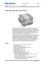
PRODUCT SPECIFICATION AC500 GAN<br />
Kari Mäki 11.4.2012 1(6)<br />
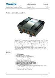
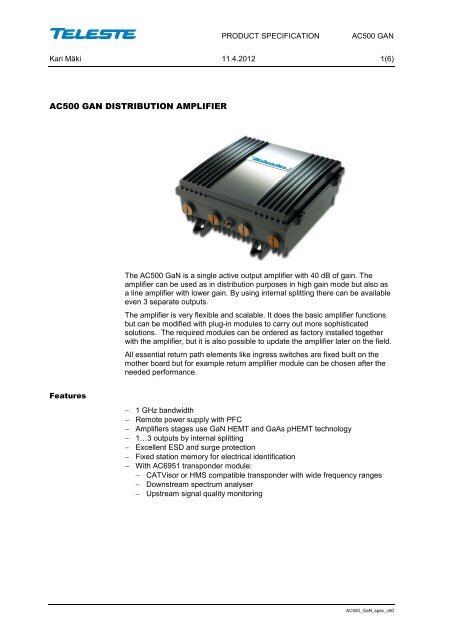
AC500 GAN DISTRIBUTION AMPLIFIER<br />
The AC500 GaN is a single active output amplifier with 40 dB of gain. The<br />
amplifier can be used as in distribution purposes in high gain mode but also as<br />
a line amplifier with lower gain. By using internal splitting there can be available<br />
even 3 separate outputs.<br />
The amplifier is very flexible and scalable. It does the basic amplifier functions<br />
but can be modified with plug-in modules to carry out more sophisticated<br />
solutions. The required modules can be ordered as factory installed together<br />
with the amplifier, but it is also possible to update the amplifier later on the field.<br />
All essential return path elements like ingress switches are fixed built on the<br />
mother board but for example return amplifier module can be chosen after the<br />
needed performance.<br />
Features<br />
− 1 GHz bandwidth<br />
− Remote power supply with PFC<br />
− Amplifiers stages use GaN HEMT and GaAs pHEMT technology<br />
− 1…3 outputs by internal splitting<br />
− Excellent ESD and surge protection<br />
− Fixed station memory for electrical identification<br />
− With AC6951 transponder module:<br />
− CATVisor or HMS compatible transponder with wide frequency ranges<br />
− Downstream spectrum analyser<br />
− Upstream signal quality monitoring<br />
AC500_GaN_spec_v50
PRODUCT SPECIFICATION AC500 GAN<br />
Kari Mäki 11.4.2012 2(6)<br />
Technical <strong>specification</strong>s<br />
Parameter Specification Note<br />
Downstream signal path (values with diplex filters)<br />
Frequency range<br />
47 / 54 / 70 / 85 / 108...1006 MHz<br />
Return loss 18 dB 1)<br />
Gain 40.5 dB 2)<br />
Input attenuator control range 20 dB 3)<br />
Input equaliser control range 25 dB 3)<br />
Interstage slope 8 dB 4)<br />
Flatness ±0.5 dB 5)<br />
Group delay 2 ns 6)<br />
Test point -20 dB 7)<br />
Transponder connection -19 dB 8)<br />
Input by-pass attenuation<br />
-2 dB<br />
Noise figure 4.7 dB 9)<br />
CTB 42 channels 117.0 dBµV 10)<br />
CSO 42 channels 117.0 dBµV 10)<br />
XMOD 42 channels 114.5 dBµV 10)<br />
CTB 110 / 77 channels 79.0 / 87.0 dB 11)<br />
CSO 110 / 77 channels 74.0 / 76 dB 11)<br />
XMOD 110 / 77 channels 73.0 / 76.0 dB 11)<br />
Upstream signal path (values with diplex filters)<br />
Frequency range<br />
5...30 / 42 / 50 / 65 / 85 MHz<br />
Return loss 18 dB 12)<br />
Gain 21 / -6.0 dB 13)<br />
Ingress switching<br />
0 / -6 / < -50 dB<br />
Attenuator control range 20 dB 14)<br />
Equaliser control range 7 dB 15)<br />
Flatness ±0.5 dB 16)<br />
Test signal injection point -30 dB 17)<br />
Transponder connection -26 dB 18)<br />
Noise figure 7.5 dB 19)<br />
Output level, DIN 45004B 113.0 dBµV 19)<br />
CINR > 63 dBc 20)<br />
General<br />
Power consumption (65 / 230 V AC) 19.0 / 20.0 W 21)<br />
Supply voltage 27...65 V AC, ±33...90V DC /<br />
205…255 V AC<br />
Maximum current feed through 8.0 A / port 22)<br />
Hum modulation 70 dB 22)<br />
Resistance for remote current<br />
25 mΩ / port<br />
Input / Output connectors<br />
PG11<br />
Test point connectors<br />
F female<br />
Dimensions 245 x 255 x 100 mm h x w x d<br />
Weight<br />
3.0 kg<br />
Operating temperature -40...+55 °C<br />
Class of enclosure IP67 23)<br />
EMC<br />
EN50083-2<br />
ESD 4 kV 24)<br />
Surge 6 kV (EN 60728-3)<br />
AC500_GaN_spec_v50
PRODUCT SPECIFICATION AC500 GAN<br />
Kari Mäki 11.4.2012 3(6)<br />
Notes<br />
1) The limiting curve is defined at 40 MHz -1.5 dB / octave.<br />
2) Guaranteed maximum gain is 40.0 dB. With combined mid-stage gain and slope control<br />
possibility the amplifier can be used in low gain mode. Specified gain is defined with mid-stage<br />
equaliser without extra losses and 2 pcs of diplex filters. All other used plug modules are 0 db<br />
jumpers.<br />
2.0 dB<br />
1.0 dB<br />
0.0 dB<br />
0 dB 1 dB 2 dB 3 dB 4 dB 5 dB 6 dB 7 dB 8 dB<br />
-1.0 dB<br />
-2.0 dB<br />
-3.0 dB<br />
CTB level<br />
CSO level<br />
NF<br />
-4.0 dB<br />
-5.0 dB<br />
Mid-Stage Attenuation<br />
The picture depicts how the NF and distortion performances change if interstage gain control is<br />
used. Defined with the 8 dB sloped output and CENELEC loading. NF curve is defined at 1006<br />
MHz.<br />
3) Fixed value attenuators and equalisers are available.<br />
4) The amplifier is defined with 8 dB tilted output between 47…1006 MHz.<br />
5) Typical value. The guaranteed value is ±0.85 dB. Flatness is defined with interstage equaliser<br />
and 2 pcs of diplex filters. All other used plug modules are 0 dB jumpers. The <strong>specification</strong> is<br />
valid 2 MHz after the starting frequency of the selected diplex filter.<br />
6) Typical value for 4.43 MHz band. Measured at channel S2. At higher frequencies the<br />
performance is better.<br />
7) Output TP has a tolerance of ± 0.75 dB between 47…862 MHz and ± 1.0 dB between<br />
862…1006 MHz. The TP is defined with 0 dB plug as OUTPUT MODULE 1. This connection<br />
can be used also as an injection point for a test signal of return channel.<br />
Input TP is a transformer type with ±1.5 dB accuracy.<br />
8) This is the level difference between output 1 and transponder connection pin on the<br />
motherboard.<br />
9) Typical value at 1006 MHz with the maximum gain. The guaranteed worst case value is 1.0 dB<br />
worse. Test conditions are described in Note 2).<br />
10) EN50083-3. Amplifier output 8 dB cable equivalent sloped. All results are typical values in room<br />
temperature, which can be used in system calculations. XMOD is measured at the lowest<br />
channel.<br />
The highest recommended output level for the amplifier is 116.0 dBµV with 42 channels.<br />
11) Measured with 77 and 110 NTSC channels. Amplifier output was 12 dB linearly sloped and the<br />
used levels were at 55 / 550 / 750 / 862 MHz 35.0 / 42.5 / 45.5 / 47.0 dBmV. All results are<br />
typical values in room temperature, which can be used in system calculations. XMOD is<br />
measured at 55.25 MHz.<br />
The highest recommended output level for the amplifier is 54 dBmV with 110 channels and 56<br />
dBmV with 77 channels.<br />
12) Valid over the band 7…65 MHz.<br />
13) Active (AC6144) / passive (AC6140) return module.<br />
14) Upstream signal path input and output have JDA9xx series attenuator plug-in slots.<br />
The upstream input attenuator factory default is JDA900.<br />
AC500_GaN_spec_v50
PRODUCT SPECIFICATION AC500 GAN<br />
Kari Mäki 11.4.2012 4(6)<br />
15) The pivot point is 65 MHz. In 30 MHz operation the equaliser control range is 3.5 dB lower.<br />
Thus the maximum gain in 30 MHz operation is 3.5 dB lower if maximum slope is used.<br />
16) Valid with active return module AC6144.<br />
17) The –30 dB level is calculated from the return signal input at output port 1, with 0 dB plugs in<br />
Output module 1 and return input attenuator slots. This 2-way connection can be used as an<br />
input test point for return signal and as a test signal injection point.<br />
18) This is the theoretical level difference between the input connector of the return signal path and<br />
the injection pin of the up-stream signal of the transponder.<br />
19) Typical values which can be used in network design. Valid with the active module AC6144.<br />
20)<br />
CINR<br />
70.0 dB<br />
65.0 dB<br />
60.0 dB<br />
55.0 dB<br />
50.0 dB<br />
45.0 dB<br />
40.0 dB<br />
-20 -15 -10 -5 0 5 10 15 20 25<br />
Input Level (dBuV / Hz)<br />
Measurement is done at 49 MHz with loading of 5 * 64QAM (6.875 Msymb/s) . AC6144 active<br />
return module was used.<br />
21) With the passive return path. With active return path and transponder the value is 4.5 W<br />
higher.<br />
22) At any frequency from 10 to 862 MHz when the remote current is less than 8 A. 12 A is the<br />
maximum total current which can be locally injected into all ports simultaneously.<br />
23) The housing is tested to be class of IP67. However, in standard delivery condition the lowest<br />
side wall is equipped with a 1 mm ventilation hole. Then the practical enclosure class is IP54.<br />
24) EN61000-4-2, contact discharge to enclosure and RF-ports.<br />
AC500_GaN_spec_v50
PRODUCT SPECIFICATION AC500 GAN<br />
Kari Mäki 11.4.2012 5(6)<br />
Monitoring functions with AC6951/-52 transponder<br />
Block Diagram<br />
− Status LEDs for alarm and modem status indication<br />
− CATVisor and HMS compatible remote connection for monitoring and control<br />
− Return path ingress switch ON / -6 dB / OFF control<br />
− 65 VAC voltage measurement with alarms<br />
− Local +12 V and +24 V voltage measurements with alarms<br />
− Internal temperature measurement with alarms<br />
− Lid status monitoring with alarm<br />
− Service terminal connection monitoring with alarm<br />
− Configuration change monitoring with alarm<br />
− Modem receive and transmit signal level monitoring with alarms<br />
− Fully user configurable alarm limits, severities, enabling and delays<br />
− Configuration data and user notes stored in motherboard memory<br />
− Uptime, total uptime and reset counters for power outage statistics<br />
− Alarm log stored into non-volatile memory for easy troubleshooting<br />
− Fast local softwate update via USB also without power supply<br />
− Remote software update to multiple units simultaneously<br />
− Spectrum analyser for downstream level measurement with alarm<br />
− Ingress analyser for upstream level measurement with alarms<br />
dB<br />
Transponder<br />
Tuner<br />
CPU<br />
RX<br />
TX<br />
Mem<br />
Tp / test<br />
injection<br />
dB<br />
dB<br />
dB<br />
0 / -6 /-50dB<br />
Tp<br />
Input<br />
module<br />
Output<br />
module 2<br />
Output<br />
module 1<br />
Tp / test<br />
injection<br />
IN<br />
AC AC OUT 3 / AC AC<br />
INPUT BYPASS OUT 2 OUT 1<br />
AC500_GaN_spec_v50
PRODUCT SPECIFICATION AC500 GAN<br />
Kari Mäki 11.4.2012 6(6)<br />
Ordering Information<br />
For ordering 1 GHz 40 dB GaN platform use selection 9-2:J<br />
AC500 configuration map<br />
1- 2- 3- 4- 5- 6- 7- 8-<br />
1 2 3 4 1 2 3 1 3 1 2 3 1 2 1 3 1 2 1 1 2<br />
AC500 - - - - - - - -<br />
1-1 Input connection (first from left) 5-1 Return path input module<br />
A PG11 A 0 dB plug (JDA900)<br />
B 5/8" B HPF 15 MHz, ingress blocker (AC6223)<br />
C IEC F LPF 30 MHz, used with optical TX (AC6210)<br />
D 3.5/12 G LPF 42 MHz, used with optical TX (AC6212)<br />
E F H LPF 50 MHz, used with optical TX (AC6215)<br />
1-2 Input by-pass/output 3 connection I LPF 65 MHz, used with optical TX (AC6217)<br />
A PG11 X None<br />
B 5/8" 5-2 Return path unit<br />
C IEC A Active return (AC6144) without att. and equal.<br />
D 3.5/12 B Active return (AC6144) with 0 dB att. and equal. (2 x JDA900)<br />
E F E Passive return (AC6140) without att. and equal.<br />
X None (PG11 sealing plug) F Passive return (AC6140) with 0 dB att. and equal. (2 x JDA900)<br />
1-3 Output 2 connection I Active return with gain and slope adjustment (AC6136)<br />
A PG11 X None<br />
B 5/8"<br />
C IEC 6-1 NA<br />
D 3.5/12 XX None<br />
E F 6-3 NA<br />
X None (PG11 sealing plug) X None<br />
1-4 Output 1 connection (first from right)<br />
A PG11 7-1 NA<br />
B 5/8" X None<br />
C IEC 7-2 NA<br />
D 3.5/12 X None<br />
E F (KDC313)<br />
8-1 Element management transponder<br />
2-1 Input module G Standard, CATVisor (AC6951)<br />
A 0 dB, no by-pass (AC6110) H Standard, HMS (AC6951 HMS)<br />
B Splitter -3.7 dB, by-pass in use (AC6124) I Standard, CATVisor (AC6911)<br />
C Tap -8 dB, by-pass in use (AC6128) J Standard, HMS (AC6911 HMS)<br />
D Tap -12 dB, by-pass in use (AC6112) X None<br />
E Tap -16 dB, by-pass in use (AC6116)<br />
F Tap -20 dB, by-pass in use (AC6119) 9-1 Power supply<br />
X None A Local powering, euro plug (230 VAC)<br />
2-2 Diplexer filters B Remote powering with cable clamp (65 VAC)<br />
A 30/47 MHz (2 x CXF030) C Local powering, UK plug (230 VAC)<br />
B 42/54 MHz (2 x CXF042) 9-2 Gain and housing<br />
C 50/70 MHz (2 x CXF050) I 39 dB, 1 GHz platform<br />
D 65/85 MHz (2 x CXF065)<br />
F 85/108 MHz (2 x CXF085)<br />
K Forward path jumper (2 x CXF000)<br />
X None<br />
2-3 Input attenuator and equaliser<br />
A 2 x 0 dB plugs (JDA900 and TXA000)<br />
B Manual gain and slope adjustment (AC6171)<br />
X None<br />
3-1 NA<br />
XX None<br />
3-3 NA<br />
X None<br />
9-<br />
4-1 Interstage slope and gain adjustment<br />
A 8 dB slope @ 862 MHz (TDE810) DOC0010326, Rev025<br />
B 8 dB slope @ 862 MHz, temp. comp. (TTE810)<br />
D 8 dB slope @ 862 MHz, -4 dB att. (TDE810 04)<br />
F 8 dB slope @ 862 MHz, -8 dB att. (TDE810 08)<br />
G Flat response (TXA000)<br />
I 8 dB slope @ 1006 MHz (TGE010<br />
X None<br />
4-2 Output module 1<br />
A 0 dB, 1 output in use (AC6120)<br />
B Splitter -3.7 dB, 2 outputs in use (AC6124)<br />
C Tap -8 dB, 2 outputs in use (AC6128)<br />
D Tap -12 dB, 2 outputs in use (AC6112)<br />
E Tap -16 dB, 2 outputs in use (AC6116)<br />
F Tap -20 dB, 2 outputs in use (AC6119)<br />
X None<br />
4-3 Output module 2<br />
A 0 dB, 2 output in use (AC6120)<br />
B Splitter -3.7 dB, 3 outputs in use (AC6124)<br />
C Tap -8 dB, 3 outputs in use (AC6128)<br />
D Tap -12 dB, 3 outputs in use (AC6112)<br />
E Tap -16 dB, 3 outputs in use (AC6116)<br />
F Tap -20 dB, 3 outputs in use (AC6119)<br />
X None<br />
AC500_GaN_spec_v50