SKM 195 GAL 062 D - Fusibles y Semiconductores Profesionales
SKM 195 GAL 062 D - Fusibles y Semiconductores Profesionales
SKM 195 GAL 062 D - Fusibles y Semiconductores Profesionales

You also want an ePaper? Increase the reach of your titles
YUMPU automatically turns print PDFs into web optimized ePapers that Google loves.
Absolute Maximum Ratings<br />
Symbol Conditions 1)<br />
V CES<br />
V CGR<br />
I C<br />
I CM<br />
V GES<br />
P tot<br />
T j , (T stg )<br />
V isol<br />
humidity<br />
climate<br />
R GE = 20 kΩ<br />
T case = 25/60 °C<br />
T case = 25/60 °C; t p = 1 ms<br />
per IGBT, T case = 25 °C<br />
AC, 1 min.<br />
DIN 40 040<br />
DIN IEC 68 T.1<br />
Inverse Diode<br />
I F = –I C T case = 25/80 °C<br />
I FM = –I CM T case = 25/80 °C; t p = 1 ms<br />
I FSM t p = 10 ms; sin.; T j = 150 °C<br />
I 2 t t p = 10 ms; T j = 150 °C<br />
Values<br />
600<br />
600<br />
230 / <strong>195</strong><br />
460 / 390<br />
± 20<br />
700<br />
–40 ... +150 (125)<br />
2 500<br />
Class F<br />
40/125/56<br />
200 / 135<br />
460 / 390<br />
1 400<br />
9800<br />
Units<br />
V<br />
V<br />
A<br />
A<br />
V<br />
W<br />
°C<br />
V<br />
A<br />
A<br />
A<br />
A 2 s<br />
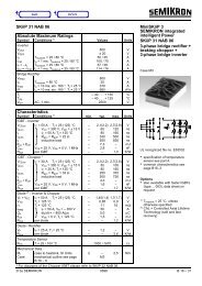
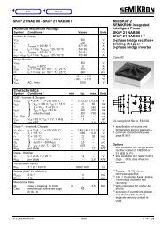
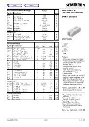
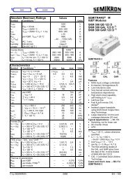
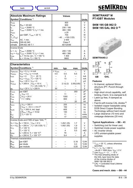
SEMITRANS ® M<br />
PT-IGBT Modules<br />
<strong>SKM</strong> <strong>195</strong> GB <strong>062</strong> D<br />
<strong>SKM</strong> <strong>195</strong> <strong>GAL</strong> <strong>062</strong> D 6)<br />
SEMITRANS 2<br />
Characteristics<br />
Symbol Conditions 1) min. typ. max. Units<br />
V (BR)CES<br />
V GE(th)<br />
I CES<br />
I GES<br />
V CEsat<br />
g fs<br />
C CHC<br />
C ies<br />
C oes<br />
C res<br />
L CE<br />
t d(on)<br />
t r<br />
t d(off)<br />
t f<br />
E on<br />
E off<br />
V GE = 0, I C = 4 mA<br />
V GE = V CE , I C = 4 mA<br />
V GE = 0 T j = 25 °C<br />
V CE = V CES T j = 125 °C<br />
V GE = 20 V, V CE = 0<br />
I C = 200 A V GE = 15 V;<br />
T j = 25 (125) °C<br />
V CE = 20 V, I C = 200 A<br />
per IGBT<br />
V GE = 0<br />
V CE = 25 V<br />
f = 1 MHz<br />
V CC = 300 V<br />
V GE = –15 V / +15 V 3)<br />
I C = 200 A, ind. load<br />
R Gon = R Goff = 10 Ω<br />
T j = 125 °C<br />
≥ V CES<br />
4,5<br />
–<br />
–<br />
–<br />
–<br />
–<br />
50<br />
–<br />
Inverse Diode and FWD of type “<strong>GAL</strong>” 8)<br />
V F = V EC I F = 150 A V GE = 0 V;<br />
Q rr I F = 200 A; T j = 125 °C 2) –<br />
V F = V EC I F = 200 A T j = 25 (125) °C<br />
–<br />
V TO<br />
r t<br />
T j = 125 °C<br />
T j = 125 °C<br />
–<br />
–<br />
I RRM I F = 200 A; T j = 125 °C 2)<br />
–<br />
Thermal characteristics<br />
R thjc<br />
R thjc<br />
R thch<br />
per IGBT<br />
per diode<br />
per module<br />
–<br />
–<br />
–<br />
–<br />
–<br />
–<br />
–<br />
–<br />
–<br />
–<br />
–<br />
–<br />
–<br />
–<br />
–<br />
5,5<br />
3<br />
13<br />
–<br />
2,1(2,2)<br />
–<br />
–<br />
–<br />
11<br />
1300<br />
800<br />
–<br />
200<br />
150<br />
600<br />
140<br />
11<br />
17<br />
1,45(1,35)<br />
1,55(1,55)<br />
–<br />
4<br />
70<br />
9,4<br />
–<br />
–<br />
–<br />
–<br />
6,5<br />
–<br />
–<br />
1<br />
2,55(2,65)<br />
–<br />
–<br />
350<br />
–<br />
–<br />
–<br />
20<br />
–<br />
–<br />
–<br />
–<br />
–<br />
–<br />
1,7<br />
1,9<br />
0,9<br />
5,5<br />
–<br />
–<br />
0,18<br />
0,3<br />
0,05<br />
V<br />
V<br />
mA<br />
mA<br />
µA<br />
V<br />
V<br />
S<br />
pF<br />
nF<br />
pF<br />
pF<br />
nH<br />
ns<br />
ns<br />
ns<br />
ns<br />
mWs<br />
mWs<br />
V<br />
V<br />
V<br />
mΩ<br />
A<br />
µC<br />
°C/W<br />
°C/W<br />
°C/W<br />
GB<br />
6)<br />
<strong>GAL</strong><br />
Features<br />
• N channel, epitaxial Silicon<br />
structure (PT- Punch-through<br />
IGBT)<br />
• High short circuit capability, self<br />
limiting, if term. G is clamped to E<br />
• Latch-up free, if clamped as<br />
above<br />
• Fast & soft inverse CAL diodes 8)<br />
• Isolated copper baseplate using<br />
DCB Direct Copper Bonding<br />
Technology without hard mould<br />
• Large clearance (10 mm) and<br />
creepage distances (20 mm)<br />
Typical Applications → B6 – 43<br />
• Switching (not for linear use)<br />
• Switched mode power supplies<br />
• AC inverter drives<br />
• UPS uninterruptable power<br />
supplies<br />
1) T case = 25 °C, unless otherwise<br />
specified<br />
2) I F = – I C , V R = 300 V,<br />
–di F /dt = 1000 A/µs, V GE = 0 V<br />
3) Use V GEoff = – 5 ... – 15 V<br />
6) The free-wheeling diode of<br />
the <strong>GAL</strong> type have the data<br />
of the inverse diodes of<br />
<strong>SKM</strong> <strong>195</strong> GB <strong>062</strong> D<br />
8) CAL = Controlled Axial Lifetime<br />
Technology<br />
Cases and mech. data → B6 – 44<br />
© by SEMIKRON 0898 B 6 – 39
<strong>SKM</strong> <strong>195</strong> GB <strong>062</strong> D ...<br />
800<br />
W<br />
700<br />
600<br />
M<strong>195</strong>G<strong>062</strong>.XLS-1<br />
mWs<br />
40<br />
30<br />
M<strong>195</strong>G<strong>062</strong>.XLS-2<br />
E off<br />
E on<br />
T j = 125 °C<br />
V CE = 600 V<br />
V GE = + 15 V<br />
R G = 10 Ω<br />
500<br />
400<br />
20<br />
300<br />
200<br />
10<br />
P tot<br />
100<br />
0<br />
0 20 40 60 80 100 120 140 160<br />
T C °C<br />
E<br />
0<br />
0 100 200 300 400 500<br />
I C<br />
A<br />
Fig. 1 Rated power dissipation P tot = f (T C ) Fig. 2 Turn-on /-off energy = f (I C )<br />
mWs<br />
E<br />
40<br />
30<br />
20<br />
10<br />
0<br />
M<strong>195</strong>G<strong>062</strong>.XLS-3<br />
E on<br />
E off<br />
0 20 40 60 80 100<br />
R G<br />
Ω<br />
T j = 125 °C<br />
V CE = 600 V<br />
V GE = + 15 V<br />
I C = 200 A<br />
1000<br />
100<br />
10<br />
I C<br />
A<br />
1<br />
M<strong>195</strong>G<strong>062</strong>.XLS-4<br />
t p =20µs<br />
100µs<br />
1ms<br />
10ms<br />
1 10 100 1000 10000<br />
V CE<br />
V<br />
1 pulse<br />
T C = 25 °C<br />
T j ≤ 150 °C<br />
Not for<br />
linear use<br />
Fig. 3 Turn-on /-off energy = f (R G ) Fig. 4 Maximum safe operating area (SOA) I C = f (V CE )<br />
2,5<br />
2<br />
1,5<br />
M<strong>195</strong>G<strong>062</strong>.XLS-5<br />
T j ≤ 150 °C<br />
V GE = 15 V<br />
R Goff = 10 Ω<br />
I C = 200 A<br />
12<br />
10<br />
8<br />
6<br />
di/dt= 200 A/µs<br />
600 A/µs<br />
1000 A/µs<br />
2000 A/µs<br />
M<strong>195</strong>G<strong>062</strong>.XLS-6<br />
T j ≤ 150 °C<br />
V GE = ± 15 V<br />
t sc ≤ 10 µs<br />
L < 25 nH<br />
I C = 200 A<br />
1<br />
4<br />
allowed numbers of<br />
short circuits: 1s<br />
I Cpuls /I C<br />
I CSC /I C<br />
0<br />
0 100 200 300 400 500 600 700<br />
V CE<br />
V<br />
0<br />
0 100 200 300 400 500 600 700<br />
V CE<br />
V<br />
Fig. 5 Turn-off safe operating area (RBSOA) Fig. 6 Safe operating area at short circuit I C = f (V CE )<br />
B 6 – 40<br />
0898<br />
© by SEMIKRON
250<br />
A<br />
200<br />
150<br />
100<br />
50<br />
I C<br />
0<br />
M<strong>195</strong>G<strong>062</strong>.XLS-8<br />
0 20 40 60 80 100 120 140 160<br />
T C °C<br />
Fig. 8 Rated current vs. temperature I C = f (T C )<br />
T j = 150 °C<br />
V GE ≥ 15V<br />
400<br />
A<br />
350<br />
300<br />
250<br />
200<br />
17V<br />
15V<br />
13V<br />
11V<br />
9V<br />
7V<br />
M<strong>195</strong>G<strong>062</strong>.XLS-9<br />
400<br />
A<br />
350<br />
300<br />
250<br />
200<br />
17V<br />
15V<br />
13V<br />
11V<br />
9V<br />
7V<br />
M<strong>195</strong>G<strong>062</strong>.XLS-10<br />
150<br />
150<br />
100<br />
100<br />
50<br />
I C<br />
0<br />
0 1 2 3 4 5<br />
V CE<br />
V<br />
50<br />
I C<br />
0<br />
0 1 2 3 4 5<br />
V CE<br />
V<br />
Fig. 9 Typ. output characteristic, t p = 250 µs; 25 °C Fig. 10 Typ. output characteristic, t p = 250 µs; 125 °C<br />
P cond(t) = V CEsat(t) · I C(t)<br />
400<br />
A<br />
350<br />
M<strong>195</strong>G<strong>062</strong>.XLS-12<br />
V CEsat(t) = V CE(TO)(Tj) + r CE(Tj) · I C(t)<br />
V CE(TO)(Tj) ≤ 1,3 – 0,003 (T j –25) [V]<br />
300<br />
250<br />
200<br />
typ.: r CE(Tj) = 0,0041 + 0,000021 (T j –25) [Ω]<br />
max.: r CE(Tj) = 0,0064 + 0,000021 (T j –25) [Ω]<br />
valid for V GE = + 15<br />
+2<br />
–1<br />
[V]; I C > 0,3 I Cnom<br />
Fig. 11 Saturation characteristic (IGBT)<br />
Calculation elements and equations<br />
150<br />
100<br />
50<br />
I C<br />
0<br />
0 2 4 6 8 10 12 14<br />
V GE<br />
V<br />
Fig. 12 Typ. transfer characteristic, t p = 250 µs; V CE = 20 V<br />
© by SEMIKRON 0898<br />
B 6 – 41
<strong>SKM</strong> <strong>195</strong> GB <strong>062</strong> D ...<br />
M<strong>195</strong>G<strong>062</strong>.XLS-13<br />
M<strong>195</strong>G<strong>062</strong>.XLS-14<br />
V<br />
20<br />
I Cpuls = 200 A<br />
100<br />
V GE = 0 V<br />
18<br />
nF<br />
f = 1 MHz<br />
Fig. 13 Typ. gate charge characteristic Fig. 14 Typ. capacitances vs.V CE<br />
16<br />
14<br />
12<br />
100V<br />
300V<br />
10<br />
C ies<br />
10<br />
8<br />
1<br />
C oes<br />
6<br />
4<br />
C res<br />
2<br />
C<br />
V GE<br />
0<br />
0,1<br />
0 0,2 0,4 0,6 0,8 1 1,2 1,4 1,6<br />
0 10 20 30<br />
V<br />
Q CE<br />
V<br />
Gate µC<br />
1000<br />
ns<br />
t don<br />
M<strong>195</strong>G<strong>062</strong>.XLS-15<br />
t doff<br />
T j = 125 °C<br />
V CE = 600 V<br />
V GE = ± 15 V<br />
R Gon = 10 Ω<br />
R Goff = 10 Ω<br />
induct. load<br />
10000<br />
ns<br />
1000<br />
M<strong>195</strong>G<strong>062</strong>.XLS-16<br />
t doff<br />
t don<br />
T j = 125 °C<br />
V CE = 600 V<br />
V GE = ± 15 V<br />
I C = 200 A<br />
induct. load<br />
100<br />
t f<br />
t r<br />
t r<br />
100<br />
t f<br />
t<br />
t<br />
10<br />
0 100 200 300 400 500<br />
I C<br />
A<br />
Fig. 15 Typ. switching times vs. I C<br />
10<br />
0 20 40 60 80 100<br />
R G<br />
Ω<br />
Fig. 16 Typ. switching times vs. gate resistor R G<br />
200<br />
A<br />
150<br />
T j =125°C, typ.<br />
T j =25°C, typ.<br />
M<strong>195</strong>G<strong>062</strong>.XLS-17<br />
mJ<br />
2,5<br />
2<br />
M<strong>195</strong>G<strong>062</strong>.XLS-18<br />
R G =<br />
5 Ω<br />
V R = 300 V<br />
T j = 125 °C<br />
V GE = ± 15 V<br />
1,5<br />
10 Ω<br />
100<br />
24 Ω<br />
50<br />
T j =125°C, max.<br />
T j =25°C, max.<br />
1<br />
0,5<br />
43 Ω<br />
75 Ω<br />
I F<br />
0<br />
0 0,4 0,8 1,2 1,6 2<br />
V F<br />
V<br />
E offD<br />
0<br />
0 50 100 150 200 250<br />
I F<br />
A<br />
Fig. 17 Typ. CAL diode forward characteristic<br />
Fig. 18 Diode turn-off energy dissipation per pulse<br />
B 6 – 42<br />
0898<br />
© by SEMIKRON
1<br />
M<strong>195</strong>G<strong>062</strong>.XLS-19<br />
1<br />
M<strong>195</strong>G<strong>062</strong>.XLS-20<br />
K/W<br />
K/W<br />
0,1<br />
0,1<br />
0,01<br />
0,001<br />
Z thJC<br />
0,01<br />
single pulse<br />
D=0,50<br />
0,20<br />
0,10<br />
0,05<br />
0,02<br />
0,01<br />
0,0001<br />
0,00001 0,0001 0,001 0,01 0,1 1<br />
t p<br />
s<br />
Fig. 19 Transient thermal impedance of IGBT<br />
Z thJC = f (t p ); D = t p / t c = t p · f<br />
0,001<br />
0,0001<br />
Z thJC<br />
single pulse<br />
D=0,5<br />
0,2<br />
0,1<br />
0,05<br />
0,02<br />
0,01<br />
0,00001<br />
0,00001 0,0001 0,001 0,01 0,1 1<br />
t<br />
s<br />
p<br />
Fig. 20 Transient thermal impedance of<br />
inverse CAL diodes Z thJC = f (t p ); D = t p / t c = t p · f<br />
A<br />
120<br />
100<br />
M<strong>195</strong>G<strong>062</strong>.XLS-22<br />
R G =<br />
5 Ω<br />
10 Ω<br />
V R = 300 V<br />
T j = 125 °C<br />
V GE = ± 15 V<br />
A<br />
120<br />
100<br />
10 Ω<br />
M<strong>195</strong>G<strong>062</strong>.XLS-23<br />
R G = 5 Ω<br />
V R = 300 V<br />
T j = 125 °C<br />
V GE = ± 15 V<br />
I F = 200 A<br />
80<br />
60<br />
24 Ω<br />
43 Ω<br />
75 Ω<br />
80<br />
60<br />
75 Ω<br />
43 Ω<br />
24 Ω<br />
40<br />
40<br />
20<br />
20<br />
I RR<br />
0<br />
0 50 100 150 200 250<br />
I F<br />
A<br />
Fig. 22 Typ. CAL diode peak reverse recovery<br />
current I RR = f (I F ; R G )<br />
Typical Applications<br />
include<br />
Switched mode power supplies<br />
DC servo and robot drives<br />
Inverters<br />
DC choppers<br />
AC motor speed control<br />
UPS Uninterruptable power supplies<br />
General power switching applications<br />
I RR<br />
0<br />
14<br />
µC<br />
Q rr<br />
12<br />
10<br />
8<br />
6<br />
4<br />
2<br />
0<br />
0 500 1000 1500 2000<br />
di F/ dt<br />
A/µs<br />
Fig. 23 Typ. CAL diode peak reverse recovery<br />
current I RR = f (di/dt)<br />
75 A<br />
50 A<br />
M<strong>195</strong>G<strong>062</strong>.XLS-24<br />
R G =<br />
I F =<br />
5 Ω<br />
10 Ω 200 A<br />
24 Ω<br />
43 Ω<br />
150 A<br />
75 Ω<br />
100 A<br />
0 500 1000 1500 2000 2500<br />
di F /dt<br />
A/µs<br />
V R = 300 V<br />
T j = 125 °C<br />
V GE = ± 15 V<br />
Fig. 24 Typ. CAL diode recovered charge<br />
© by SEMIKRON 0898<br />
B 6 – 43
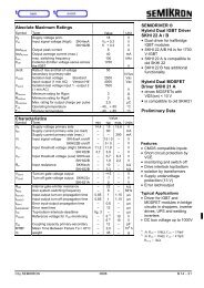
<strong>SKM</strong> <strong>195</strong> GB <strong>062</strong> D ...<br />
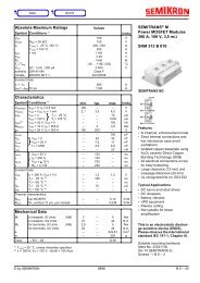
SEMITRANS 2<br />
Case D 61<br />
UL Recognized<br />
File no. E 63 532<br />
<strong>SKM</strong> <strong>195</strong> GB <strong>062</strong> D<br />
Dimensions in mm<br />
Case outline and circuit diagram<br />
Mechanical Data<br />
Symbol Conditions Values Units<br />
min. typ. max.<br />
M 1<br />
M 2<br />
a<br />
w<br />
to heatsink, SI Units(M6)<br />
to heatsink, US Units<br />
for terminals, SI Units(M5)<br />
for terminals, US Units<br />
3<br />
27<br />
2,5<br />
22<br />
–<br />
–<br />
–<br />
–<br />
–<br />
–<br />
–<br />
–<br />
5<br />
44<br />
5<br />
44<br />
5x9,81<br />
160<br />
Nm<br />
lb.in.<br />
Nm<br />
lb.in.<br />
m/s 2<br />
g<br />
This is an electrostatic discharge<br />
sensitive device (ESDS).<br />
Please observe the international<br />
standard IEC 747-1, Chapter IX.<br />
Eight devices are supplied in one<br />
SEMIBOX A without mounting hardware,<br />
which can be ordered separately<br />
under Ident No. 33321100 (for<br />
10 SEMITRANS 2)<br />
Larger packing units of 20 or 42 pieces<br />
are used if suitable<br />
Accessories → B 6 – 4<br />
SEMIBOX → C - 1.<br />
B 6 – 44<br />
0898<br />
© by SEMIKRON