SL3S1203_1213 UCODE G2iL and G2iL+ - AdvanIDe
SL3S1203_1213 UCODE G2iL and G2iL+ - AdvanIDe
SL3S1203_1213 UCODE G2iL and G2iL+ - AdvanIDe

You also want an ePaper? Increase the reach of your titles
YUMPU automatically turns print PDFs into web optimized ePapers that Google loves.
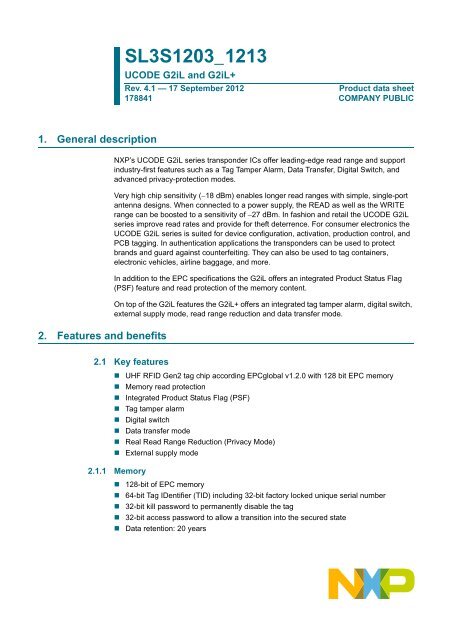
<strong>SL3S1203</strong>_<strong>1213</strong><br />
<strong>UCODE</strong> <strong>G2iL</strong> <strong>and</strong> <strong>G2iL</strong>+<br />
Rev. 4.1 — 17 September 2012<br />
178841<br />
Product data sheet<br />
COMPANY PUBLIC<br />
1. General description<br />
NXP’s <strong>UCODE</strong> <strong>G2iL</strong> series transponder ICs offer leading-edge read range <strong>and</strong> support<br />
industry-first features such as a Tag Tamper Alarm, Data Transfer, Digital Switch, <strong>and</strong><br />
advanced privacy-protection modes.<br />
Very high chip sensitivity (18 dBm) enables longer read ranges with simple, single-port<br />
antenna designs. When connected to a power supply, the READ as well as the WRITE<br />
range can be boosted to a sensitivity of 27 dBm. In fashion <strong>and</strong> retail the <strong>UCODE</strong> <strong>G2iL</strong><br />
series improve read rates <strong>and</strong> provide for theft deterrence. For consumer electronics the<br />
<strong>UCODE</strong> <strong>G2iL</strong> series is suited for device configuration, activation, production control, <strong>and</strong><br />
PCB tagging. In authentication applications the transponders can be used to protect<br />
br<strong>and</strong>s <strong>and</strong> guard against counterfeiting. They can also be used to tag containers,<br />
electronic vehicles, airline baggage, <strong>and</strong> more.<br />
In addition to the EPC specifications the <strong>G2iL</strong> offers an integrated Product Status Flag<br />
(PSF) feature <strong>and</strong> read protection of the memory content.<br />
On top of the <strong>G2iL</strong> features the <strong>G2iL</strong>+ offers an integrated tag tamper alarm, digital switch,<br />
external supply mode, read range reduction <strong>and</strong> data transfer mode.<br />
2. Features <strong>and</strong> benefits<br />
2.1 Key features<br />
• UHF RFID Gen2 tag chip according EPCglobal v1.2.0 with 128 bit EPC memory<br />
• Memory read protection<br />
• Integrated Product Status Flag (PSF)<br />
• Tag tamper alarm<br />
• Digital switch<br />
• Data transfer mode<br />
• Real Read Range Reduction (Privacy Mode)<br />
• External supply mode<br />
2.1.1 Memory<br />
• 128-bit of EPC memory<br />
• 64-bit Tag IDentifier (TID) including 32-bit factory locked unique serial number<br />
• 32-bit kill password to permanently disable the tag<br />
• 32-bit access password to allow a transition into the secured state<br />
• Data retention: 20 years
NXP Semiconductors<br />
<strong>SL3S1203</strong>_<strong>1213</strong><br />
<strong>UCODE</strong> <strong>G2iL</strong> <strong>and</strong> <strong>G2iL</strong>+<br />
• Broad international operating frequency: from 840 MHz to 960 MHz<br />
• Long read/write ranges due to extremely low power design<br />
• Reliable operation of multiple tags due to advanced anti-collision<br />
• READ protection<br />
• WRITE Lock<br />
• Wide specified temperature range: 40 C up to +85 C<br />
2.2 Key benefits<br />
2.2.1 End user benefit<br />
• Prevention of unauthorized memory access through read protection<br />
• Indication of tag tampering attempt by use of the tag tamper alarm feature<br />
• Electronic device configuration <strong>and</strong> / or activation by the use of the digital switch / data<br />
transfer mode<br />
• Theft deterrence supported by the PSF feature (PSF alarm or EPC code)<br />
• Small label sizes, long read ranges due to high chip sensitivity<br />
• Product identification through unalterable extended TID range, including a 32-bit serial<br />
number<br />
• Reliable operation in dense reader <strong>and</strong> noisy environments through high interference<br />
suppression<br />
2.2.2 Antenna design benefits<br />
• High sensitivity enables small <strong>and</strong> cost efficient antenna designs<br />
• Low Q-Value eases broad b<strong>and</strong> antenna design for global usage<br />
2.2.3 Label manufacturer benefit<br />
• Consistent performance on different materials due to low Q-factor<br />
• Ease of assembly <strong>and</strong> high assembly yields through large chip input capacitance<br />
• Fast first WRITE of the EPC memory for fast label initialization<br />
2.3 Custom comm<strong>and</strong>s<br />
• PSF Alarm<br />
Built-in PSF (Product Status Flag), enables the UHF RFID tag to be used as EAS tag<br />
(Electronic Article Surveillance) tag without the need for a back-end data base.<br />
• Read Protect<br />
Protects all memory content including CRC16 from unauthorized reading.<br />
• ChangeConfig<br />
Configures the additional features of the chip like external supply mode, tamper alarm,<br />
digital switch, read range reduction or data transfer.<br />
The <strong>UCODE</strong> <strong>G2iL</strong> is equipped with a number of additional features <strong>and</strong> custom<br />
comm<strong>and</strong>s. Nevertheless, the chip is designed in a way st<strong>and</strong>ard EPCglobal<br />
READ/WRITE/ACCESS comm<strong>and</strong>s can be used to operate the features. No custom<br />
comm<strong>and</strong>s are needed to take advantage of all the features in case of unlocked EPC<br />
memory.<br />
<strong>SL3S1203</strong>_<strong>1213</strong> All information provided in this document is subject to legal disclaimers. © NXP B.V. 2012. All rights reserved.<br />
Product data sheet<br />
COMPANY PUBLIC<br />
Rev. 4.1 — 17 September 2012<br />
178841 2 of 36
NXP Semiconductors<br />
<strong>SL3S1203</strong>_<strong>1213</strong><br />
<strong>UCODE</strong> <strong>G2iL</strong> <strong>and</strong> <strong>G2iL</strong>+<br />
3. Applications<br />
3.1 Markets<br />
• Fashion (Apparel <strong>and</strong> footwear)<br />
• Retail<br />
• Electronics<br />
• Fast Moving Consumer Goods<br />
• Asset management<br />
• Electronic Vehicle Identification<br />
3.2 Applications<br />
• Supply chain management<br />
Item level tagging<br />
Pallet <strong>and</strong> case tracking<br />
• Container identification<br />
• Product authentication<br />
• PCB tagging<br />
• Cost efficient, low level seals<br />
• Wireless firmware download<br />
• Wireless product activation<br />
Outside above mentioned applications, please contact NXP Semiconductors for support.<br />
4. Ordering information<br />
Table 1. Ordering information<br />
Type number Package<br />
Name IC type Description Version<br />
<strong>SL3S1203</strong>FUF Wafer <strong>G2iL</strong> bumped die on sawn 8” 75 m wafer not applicable<br />
SL3S<strong>1213</strong>FUF Wafer <strong>G2iL</strong>+ bumped die on sawn 8” 75 m wafer not applicable<br />
<strong>SL3S1203</strong>FUD/BG Wafer <strong>G2iL</strong> bumped die on sawn 8” 120 m wafer,<br />
not applicable<br />
7 m Polyimide spacer<br />
SL3S<strong>1213</strong>FUD/BG Wafer <strong>G2iL</strong>+ bumped die on sawn 8” 120 m wafer,<br />
not applicable<br />
7 m Polyimide spacer<br />
<strong>SL3S1203</strong>FTB0 XSON6 <strong>G2iL</strong> plastic extremely thin small outline package;<br />
SOT886F1<br />
no leads; 6 terminals; body 1 1.45 0.5 mm<br />
SL3S<strong>1213</strong>FTB0 XSON6 <strong>G2iL</strong>+ plastic extremely thin small outline package;<br />
no leads; 6 terminals; body 1 1.45 0.5 mm<br />
SOT886F1<br />
<strong>SL3S1203</strong>_<strong>1213</strong> All information provided in this document is subject to legal disclaimers. © NXP B.V. 2012. All rights reserved.<br />
Product data sheet<br />
COMPANY PUBLIC<br />
Rev. 4.1 — 17 September 2012<br />
178841 3 of 36
NXP Semiconductors<br />
<strong>SL3S1203</strong>_<strong>1213</strong><br />
<strong>UCODE</strong> <strong>G2iL</strong> <strong>and</strong> <strong>G2iL</strong>+<br />
5. Marking<br />
6. Block diagram<br />
Table 2. Marking codes<br />
Type number Marking code Comment Version<br />
<strong>SL3S1203</strong>FTB0 UN <strong>UCODE</strong> <strong>G2iL</strong> SOT886<br />
SL3S<strong>1213</strong>FTB0 UQ <strong>UCODE</strong> <strong>G2iL</strong>+ SOT886<br />
The SL3S12x3 IC consists of three major blocks:<br />
- Analog Interface<br />
- Digital Control<br />
- EEPROM<br />
The analog part provides stable supply voltage <strong>and</strong> demodulates data received from the<br />
reader for being processed by the digital part. Further, the modulation transistor of the<br />
analog part transmits data back to the reader.<br />
The digital section includes the state machines, processes the protocol <strong>and</strong> h<strong>and</strong>les<br />
communication with the EEPROM, which contains the EPC <strong>and</strong> the user data.<br />
ANALOG<br />
RF INTERFACE<br />
DIGITAL CONTROL<br />
EEPROM<br />
VREG<br />
PAD<br />
VDD<br />
ANTICOLLISION<br />
ANTENNA<br />
RECT<br />
DEMOD<br />
data<br />
in<br />
READ/WRITE<br />
CONTROL<br />
MOD<br />
ACCESS CONTROL<br />
MEMORY<br />
PAD<br />
data<br />
out<br />
EEPROM INTERFACE<br />
CONTROL<br />
R/W<br />
PAD<br />
VDD<br />
OUT<br />
PAD<br />
I/O<br />
CONTROL<br />
RF INTERFACE<br />
CONTROL<br />
I/O CONTROL<br />
SEQUENCER<br />
CHARGE PUMP<br />
001aam226<br />
Fig 1.<br />
Block diagram of <strong>G2iL</strong> IC<br />
<strong>SL3S1203</strong>_<strong>1213</strong> All information provided in this document is subject to legal disclaimers. © NXP B.V. 2012. All rights reserved.<br />
Product data sheet<br />
COMPANY PUBLIC<br />
Rev. 4.1 — 17 September 2012<br />
178841 4 of 36
NXP Semiconductors<br />
<strong>SL3S1203</strong>_<strong>1213</strong><br />
<strong>UCODE</strong> <strong>G2iL</strong> <strong>and</strong> <strong>G2iL</strong>+<br />
7. Pinning information<br />
OUT<br />
RFN<br />
SL3S12x3FTB0<br />
RFP<br />
1<br />
6<br />
VDD<br />
n.c.<br />
2<br />
5<br />
n.c.<br />
VDD<br />
NXP trademark<br />
RFP<br />
RFN<br />
3<br />
4<br />
OUT<br />
001aan103<br />
001aam529<br />
Transparent top view<br />
Fig 2. Pinning bare die Fig 3. Pin configuration for SOT886<br />
7.1 Pin description<br />
Table 3.<br />
Symbol<br />
OUT<br />
RFN<br />
VDD<br />
RFP<br />
Pin description bare die<br />
Description<br />
output pin<br />
grounded antenna connector<br />
external supply<br />
ungrounded antenna connector<br />
Table 4. Pin description SOT886<br />
Pin Symbol Description<br />
1 RFP ungrounded antenna connector<br />
2 n.c. not connected<br />
3 RFN grounded antenna connector<br />
4 OUT output pin<br />
5 n.c. not connected<br />
6 VDD external supply<br />
<strong>SL3S1203</strong>_<strong>1213</strong> All information provided in this document is subject to legal disclaimers. © NXP B.V. 2012. All rights reserved.<br />
Product data sheet<br />
COMPANY PUBLIC<br />
Rev. 4.1 — 17 September 2012<br />
178841 5 of 36
NXP Semiconductors<br />
<strong>SL3S1203</strong>_<strong>1213</strong><br />
<strong>UCODE</strong> <strong>G2iL</strong> <strong>and</strong> <strong>G2iL</strong>+<br />
8. Wafer layout<br />
8.1 Wafer layout<br />
(1)<br />
OUT<br />
RFN<br />
(5)<br />
Y<br />
(6) (4)<br />
(7)<br />
X<br />
VDD<br />
(8)<br />
RFP<br />
(2)<br />
(3)<br />
not to scale!<br />
001aak871<br />
(1) Die to Die distance (metal sealring - metal sealring) 21,4 m, (X-scribe line width: 15 m)<br />
(2) Die to Die distance (metal sealring - metal sealring) 21,4 m, (Y-scribe line width: 15 m)<br />
(3) Chip step, x-length: 485 m<br />
(4) Chip step, y-length: 435 m<br />
(5) Bump to bump distance X (OUT - RFN): 383 m<br />
(6) Bump to bump distance Y (RFN - RFP): 333 m<br />
(7) Distance bump to metal sealring X: 40,3 m (outer edge - top metal)<br />
(8) Distance bump to metal sealring Y: 40,3 m<br />
Bump size X x Y: 60 m x 60 m<br />
Remark: OUT <strong>and</strong> VDD are used with <strong>G2iL</strong>+ only<br />
Fig 4. <strong>G2iL</strong> wafer layout<br />
<strong>SL3S1203</strong>_<strong>1213</strong> All information provided in this document is subject to legal disclaimers. © NXP B.V. 2012. All rights reserved.<br />
Product data sheet<br />
COMPANY PUBLIC<br />
Rev. 4.1 — 17 September 2012<br />
178841 6 of 36
NXP Semiconductors<br />
<strong>SL3S1203</strong>_<strong>1213</strong><br />
<strong>UCODE</strong> <strong>G2iL</strong> <strong>and</strong> <strong>G2iL</strong>+<br />
9. Mechanical specification<br />
The <strong>UCODE</strong> <strong>G2iL</strong>/<strong>G2iL</strong>+ wafers are available in 75 m <strong>and</strong> 120 m thickness. The 75m<br />
thick wafer allows ultra thin label design but require a proper tuning of the glue dispenser<br />
during production. Because of the more robust structure of the 120m wafer, the wafer is<br />
ideal for harsh applications. The 120 m thick wafer is also enhanced with 7m Polyimide<br />
spacer allowing additional protection of the active circuit.<br />
9.1 Wafer specification<br />
9.1.1 Wafer<br />
See Ref. 20 “Data sheet - Delivery type description – General specification for 8” wafer on<br />
UV-tape with electronic fail die marking, BU-ID document number: 1093**”.<br />
Table 5. Specifications<br />
Wafer<br />
Designation<br />
each wafer is scribed with batch number<br />
<strong>and</strong> wafer number<br />
Diameter 200 mm (8”)<br />
Thickness<br />
SL3S12x3FUF<br />
75 m 15 m<br />
SL3S12x3FUD<br />
120 m 15 m<br />
Number of pads 4<br />
Pad location<br />
non diagonal/ placed in chip corners<br />
Distance pad to pad RFN-RFP<br />
333.0 m<br />
Distance pad to pad OUT-RFN<br />
383.0 m<br />
Process<br />
CMOS 0.14 m<br />
Batch size<br />
25 wafers<br />
Potential good dies per wafer 139.351<br />
Wafer backside<br />
Material<br />
Si<br />
Treatment<br />
ground <strong>and</strong> stress release<br />
Roughness<br />
R a max. 0.5 m, R t max. 5 m<br />
Chip dimensions<br />
Die size including scribe 0.485 mm 0.435 mm = 0.211 mm 2<br />
Scribe line width:<br />
x-dimension = 15 m<br />
y-dimension = 15 m<br />
Passivation on front<br />
Type<br />
S<strong>and</strong>wich structure<br />
Material<br />
PE-Nitride (on top)<br />
Thickness<br />
1.75 m total thickness of passivation<br />
Polyimide spacer<br />
7 m 1 m (SL3S12x3FUD only)<br />
Au bump<br />
Bump material<br />
> 99.9 % pure Au<br />
<strong>SL3S1203</strong>_<strong>1213</strong> All information provided in this document is subject to legal disclaimers. © NXP B.V. 2012. All rights reserved.<br />
Product data sheet<br />
COMPANY PUBLIC<br />
Rev. 4.1 — 17 September 2012<br />
178841 7 of 36
NXP Semiconductors<br />
<strong>SL3S1203</strong>_<strong>1213</strong><br />
<strong>UCODE</strong> <strong>G2iL</strong> <strong>and</strong> <strong>G2iL</strong>+<br />
[1] Because of the 7 m spacer, the bump will measure 18 m relative height protruding the spacer.<br />
9.1.2 Fail die identification<br />
No inkdots are applied to the wafer.<br />
Electronic wafer mapping (SECS II format) covers the electrical test results <strong>and</strong><br />
additionally the results of mechanical/visual inspection.<br />
See Ref. 20 “Data sheet - Delivery type description – General specification for 8” wafer on<br />
UV-tape with electronic fail die marking, BU-ID document number: 1093**”<br />
9.1.3 Map file distribution<br />
See Ref. 20 “Data sheet - Delivery type description – General specification for 8” wafer on<br />
UV-tape with electronic fail die marking, BU-ID document number: 1093**”<br />
10. Functional description<br />
Table 5. Specifications<br />
Bump hardness 35 – 80 HV 0.005<br />
Bump shear strength<br />
> 70 MPa<br />
Bump height<br />
SL3S12x3FUF<br />
18 m<br />
SL3S12x3FUD 25 m [1]<br />
Bump height uniformity<br />
within a die<br />
2 m<br />
– within a wafer 3 m<br />
– wafer to wafer 4 m<br />
Bump flatness<br />
1.5 m<br />
Bump size<br />
– RFP, RFN 60 60 m<br />
– OUT, VDD 60 60 m<br />
Bump size variation<br />
5 m<br />
10.1 Air interface st<strong>and</strong>ards<br />
The <strong>UCODE</strong> <strong>G2iL</strong> fully supports all parts of the "Specification for RFID Air Interface<br />
EPCglobal, EPC Radio-Frequency Identity Protocols, Class-1 Generation-2 UHF RFID,<br />
Protocol for Communications at 860 MHz to 960 MHz, Version 1.2.0".<br />
10.2 Power transfer<br />
The interrogator provides an RF field that powers the tag, equipped with a <strong>UCODE</strong> <strong>G2iL</strong>.<br />
The antenna transforms the impedance of free space to the chip input impedance in order<br />
to get the maximum possible power for the <strong>G2iL</strong> on the tag. The <strong>G2iL</strong>+ can also be<br />
supplied externally.<br />
The RF field, which is oscillating on the operating frequency provided by the interrogator,<br />
is rectified to provide a smoothed DC voltage to the analog <strong>and</strong> digital modules of the IC.<br />
<strong>SL3S1203</strong>_<strong>1213</strong> All information provided in this document is subject to legal disclaimers. © NXP B.V. 2012. All rights reserved.<br />
Product data sheet<br />
COMPANY PUBLIC<br />
Rev. 4.1 — 17 September 2012<br />
178841 8 of 36
NXP Semiconductors<br />
<strong>SL3S1203</strong>_<strong>1213</strong><br />
<strong>UCODE</strong> <strong>G2iL</strong> <strong>and</strong> <strong>G2iL</strong>+<br />
The antenna that is attached to the chip may use a DC connection between the two<br />
antenna pads. Therefore the <strong>G2iL</strong> also enables loop antenna design. Possible examples<br />
of supported antenna structures can be found in the reference antenna design guide.<br />
10.3 Data transfer<br />
10.3.1 Reader to tag Link<br />
An interrogator transmits information to the <strong>UCODE</strong> <strong>G2iL</strong> by modulating an UHF RF<br />
signal. The <strong>G2iL</strong> receives both information <strong>and</strong> operating energy from this RF signal. Tags<br />
are passive, meaning that they receive all of their operating energy from the interrogator's<br />
RF waveform. In order to further improve the read range the <strong>UCODE</strong> <strong>G2iL</strong>+ can be<br />
externally supplied as well so the energy to operate the chip does not need to be<br />
transmitted by the reader.<br />
An interrogator is using a fixed modulation <strong>and</strong> data rate for the duration of at least one<br />
inventory round. It communicates to the <strong>G2iL</strong> by modulating an RF carrier using DSB-ASK<br />
with PIE encoding.<br />
For further details refer to Section 16, Ref. 1. Interrogator-to-tag (R=>T) communications.<br />
10.3.2 Tag to reader Link<br />
An interrogator receives information from a <strong>G2iL</strong> by transmitting an unmodulated RF<br />
carrier <strong>and</strong> listening for a backscattered reply. The <strong>G2iL</strong> backscatters by switching the<br />
reflection coefficient of its antenna between two states in accordance with the data being<br />
sent. For further details refer to Section 16, Ref. 1, chapter 6.3.1.3.<br />
The <strong>UCODE</strong> <strong>G2iL</strong> communicates information by backscatter-modulating the amplitude<br />
<strong>and</strong>/or phase of the RF carrier. Interrogators shall be capable of demodulating either<br />
demodulation type.<br />
The encoding format, selected in response to interrogator comm<strong>and</strong>s, is either FM0<br />
baseb<strong>and</strong> or Miller-modulated subcarrier.<br />
10.4 <strong>G2iL</strong> <strong>and</strong> <strong>G2iL</strong>+ differences<br />
The <strong>UCODE</strong> <strong>G2iL</strong> is tailored for application where mainly EPC or TID number space is<br />
needed. The <strong>G2iL</strong>+ in addition provides functionality such as tag tamper alarm, external<br />
supply operation to further boost read/write range (external supply mode), a Privacy mode<br />
reducing the read range or I/O functionality (data transfer to externally connected devices)<br />
required.<br />
The following table provides an overview of <strong>G2iL</strong>, <strong>G2iL</strong>+ special features.<br />
Table 6. Overview of <strong>G2iL</strong> <strong>and</strong> <strong>G2iL</strong>+ features<br />
Features <strong>G2iL</strong> <strong>G2iL</strong>+<br />
Read protection (bankwise) yes yes<br />
PSF (Built-in Product Status Flag) yes yes<br />
Backscatter strength reduction yes yes<br />
Real read range reduction yes yes<br />
Digital switch / Digital input - yes<br />
<strong>SL3S1203</strong>_<strong>1213</strong> All information provided in this document is subject to legal disclaimers. © NXP B.V. 2012. All rights reserved.<br />
Product data sheet<br />
COMPANY PUBLIC<br />
Rev. 4.1 — 17 September 2012<br />
178841 9 of 36
NXP Semiconductors<br />
<strong>SL3S1203</strong>_<strong>1213</strong><br />
<strong>UCODE</strong> <strong>G2iL</strong> <strong>and</strong> <strong>G2iL</strong>+<br />
Table 6. Overview of <strong>G2iL</strong> <strong>and</strong> <strong>G2iL</strong>+ features …continued<br />
Features <strong>G2iL</strong> <strong>G2iL</strong>+<br />
External supply mode - yes<br />
Data transfer - yes<br />
Tag tamper alarm - yes<br />
10.5 Supported comm<strong>and</strong>s<br />
The <strong>G2iL</strong> supports all m<strong>and</strong>atory EPCglobal V1.2.0 comm<strong>and</strong>s.<br />
In addition the <strong>G2iL</strong> supports the following optional comm<strong>and</strong>s:<br />
• ACCESS<br />
• Block Write (32 bit), after a Req_RN comm<strong>and</strong> (see Ref. 21)<br />
The <strong>G2iL</strong> features the following custom comm<strong>and</strong>s described more in detail later:<br />
• ResetReadProtect<br />
• ReadProtect<br />
• ChangeEAS<br />
• EAS_Alarm<br />
• ChangeConfig<br />
(backward compatible to G2X)<br />
(backward compatible to G2X)<br />
(backward compatible to G2X)<br />
(backward compatible to G2X)<br />
(new with <strong>G2iL</strong>)<br />
10.6 <strong>G2iL</strong>, <strong>G2iL</strong>+ memory<br />
The <strong>G2iL</strong>, <strong>G2iL</strong>+ memory is implemented according EPCglobal Class1Gen2 <strong>and</strong><br />
organized in three sections:<br />
Table 7. <strong>G2iL</strong> memory sections<br />
Name Size Bank<br />
Reserved memory (32 bit ACCESS <strong>and</strong> 32 bit KILL password) 64 bit 00b<br />
EPC (excluding 16 bit CRC-16 <strong>and</strong> 16 bit PC) 128 bit 01b<br />
<strong>G2iL</strong> Configuration Word 16 bit 01b<br />
TID (including permalocked unique 32 bit serial number) 64 bit 10b<br />
The logical address of all memory banks begin at zero (00h).<br />
In addition to the three memory banks one configuration word to h<strong>and</strong>le the <strong>G2iL</strong> specific<br />
features is available at EPC bank 01 address 200h. The configuration word is described in<br />
detail in Section 10.7.1 “ChangeConfig”.<br />
Memory pages (16 bit words) pre-programmed to zero will not execute an erase cycle<br />
before writing data to it. This approach accelerates initialization of the chip <strong>and</strong> enables<br />
faster programming of the memory.<br />
<strong>SL3S1203</strong>_<strong>1213</strong> All information provided in this document is subject to legal disclaimers. © NXP B.V. 2012. All rights reserved.<br />
Product data sheet<br />
COMPANY PUBLIC<br />
Rev. 4.1 — 17 September 2012<br />
178841 10 of 36
NXP Semiconductors<br />
<strong>SL3S1203</strong>_<strong>1213</strong><br />
<strong>UCODE</strong> <strong>G2iL</strong> <strong>and</strong> <strong>G2iL</strong>+<br />
10.6.1 <strong>G2iL</strong>, <strong>G2iL</strong>+ overall memory map<br />
Table 8. <strong>G2iL</strong>, <strong>G2iL</strong>+ overall memory map<br />
Bank Memory Type Content Initial Remark<br />
address address<br />
Bank 00 00h to 1Fh reserved kill password all 00h unlocked memory<br />
20h to 3Fh reserved access password all 00h unlocked memory<br />
Bank 01<br />
EPC<br />
Bank 01<br />
Config Word<br />
Bank 10<br />
TID<br />
00h to 0Fh EPC CRC-16: refer to Ref. 16 memory mapped<br />
calculated CRC<br />
10h to 14h EPC backscatter length 00110b unlocked memory<br />
15h EPC UMI 0b unlocked memory<br />
16h EPC XPC indicator 0b hardwired to 0<br />
17h to 1Fh EPC numbering system indicator 00h unlocked memory<br />
20h to 9Fh EPC EPC<br />
[1]<br />
unlocked memory<br />
200h EPC tamper alarm flag 0b [4] indicator bit<br />
201h EPC external supply flag or input 0b [4]<br />
indicator bit<br />
signal<br />
202h EPC RFU 0b [4] locked memory<br />
203h EPC RFU 0b [4] locked memory<br />
204h EPC invert digital output: 0b [4] temporary bit<br />
205h EPC transparent mode on/off 0b [4] temporary bit<br />
206h EPC transparent mode data/raw 0b [4] temporary bit<br />
207h EPC RFU 0b [4] locked memory<br />
208h EPC RFU 0b [4] locked memory<br />
209h EPC max. backscatter strength 1b [4] unlocked memory<br />
20Ah EPC digital output 0b [4] unlocked memory<br />
20Bh EPC read range reduction on/off 0b [4] unlocked memory<br />
20Ch EPC RFU 0b [4] locked memory<br />
20Dh EPC read protect EPC Bank 0b [4] unlocked memory<br />
20Eh EPC read protect TID 0b [4] unlocked memory<br />
20Fh EPC PSF alarm flag 0b [4] unlocked memory<br />
00h to 07h TID allocation class identifier 1110 0010b locked memory<br />
08h to 13h TID tag mask designer identifier 0000 0000 0110b locked memory<br />
14h TID config word indicator 1b [2] locked memory<br />
14h to 1Fh TID tag model number TMNR [3] locked memory<br />
20h to 3Fh TID serial number SNR locked memory<br />
[1] <strong>G2iL</strong>: HEX E200 6806 0000 0000 0000 0000 (0000 0000)<br />
<strong>G2iL</strong>+: HEX E200 6807 0000 0000 0000 0000 (0000 0000)<br />
[2] Indicates the existence of a Configuration Word at the end of the EPC number<br />
[3] See Figure 5<br />
[4] See also Table 12 for further details.<br />
<strong>SL3S1203</strong>_<strong>1213</strong> All information provided in this document is subject to legal disclaimers. © NXP B.V. 2012. All rights reserved.<br />
Product data sheet<br />
COMPANY PUBLIC<br />
Rev. 4.1 — 17 September 2012<br />
178841 11 of 36
Product data sheet<br />
COMPANY PUBLIC<br />
Rev. 4.1 — 17 September 2012<br />
178841 12 of 36<br />
<strong>SL3S1203</strong>_<strong>1213</strong> All information provided in this document is subject to legal disclaimers. © NXP B.V. 2012. All rights reserved.<br />
Fig 5.<br />
xxxxxxxxxxxxxxxxxxxxx xxxxxxxxxxxxxxxxxxxxxxxxxx xxxxxxx x x x xxxxxxxxxxxxxxxxxxxxxxxxxxxxxx xxxxxxxxxxxxxxxxxxx xx xx xxxxx<br />
xxxxxxxxxxxxxxxxxxxxxxxxxxx xxxxxxxxxxxxxxxxxxx xxxxxx xxxxxxxxxxxxxxxxxxxxxxxxxxxxxxxxxxx xxxxxxxxxxxx x x<br />
xxxxxxxxxxxxxxxxxxxxx xxxxxxxxxxxxxxxxxxxxxxxxxxxxxx xxxxx xxxxxxxxxxxxxxxxxxxxxxxxxxxxxxxxxxxxxxxxxxxxxxxxxx xxxxxxxx<br />
xxxxxxxxxxxxxxxxxxxxxxxxx xxxxxxxxxxxxxxxxxxxx xxx<br />
10.6.2 <strong>G2iL</strong> TID memory details<br />
Addresses<br />
MS Bit<br />
00h<br />
MS Byte<br />
LS Bit<br />
Class Identifier<br />
<strong>G2iL</strong> TID memory structure<br />
First 32 bit of TID<br />
memory<br />
Class ID<br />
Mask<br />
Designer<br />
ID<br />
Config<br />
Word<br />
Indicator<br />
Model Number<br />
Sub<br />
Version Nr.<br />
Version<br />
(Silicon) Nr.<br />
Ucode <strong>G2iL</strong> E2006806 E2h 006h 1 0000b 0000110b<br />
Ucode <strong>G2iL</strong>+ E2006807 E2h 006h 1 0000b 0000111b<br />
Addresses 00h<br />
Mask-Designer Identifier Model Number Serial Number<br />
TID<br />
MS Bit<br />
LS Byte<br />
07h 08h 13h 14h 1Fh 20h<br />
3Fh<br />
Bits 7<br />
0 11 0 11 0 31<br />
0<br />
E2h<br />
006h<br />
806h<br />
00000001h to FFFFFFFFh<br />
(EAN.UCC)<br />
(NXP)<br />
(<strong>UCODE</strong> <strong>G2iL</strong>)<br />
Addresses 14h<br />
Sub Version Number<br />
Bits 0 3<br />
0<br />
000b<br />
18h 19h<br />
Version Number<br />
6 0<br />
0000110b<br />
(<strong>UCODE</strong> <strong>G2iL</strong>)<br />
1Fh<br />
3Fh<br />
LS Bit<br />
001aam227<br />
<strong>UCODE</strong> <strong>G2iL</strong> <strong>and</strong> <strong>G2iL</strong>+<br />
NXP Semiconductors <strong>SL3S1203</strong>_<strong>1213</strong>
NXP Semiconductors<br />
<strong>SL3S1203</strong>_<strong>1213</strong><br />
<strong>UCODE</strong> <strong>G2iL</strong> <strong>and</strong> <strong>G2iL</strong>+<br />
10.7 Custom comm<strong>and</strong>s<br />
The <strong>UCODE</strong> <strong>G2iL</strong>, <strong>G2iL</strong>+ is equipped with a number of additional features <strong>and</strong> custom<br />
comm<strong>and</strong>s.<br />
Nevertheless, the chip is designed in a way st<strong>and</strong>ard EPCglobal READ/WRITE/ACCESS<br />
comm<strong>and</strong>s can be used to operate the features.<br />
The memory map stated in the previous section describes the Configuration Word used to<br />
control the additional features located at address 200h of the EPC memory. For this<br />
reason the st<strong>and</strong>ard READ/WRITE comm<strong>and</strong>s of an UHF EPCglobal compliant reader<br />
can be used to select the flags or activate/deactivate features.<br />
The features can only be activated/deactivated (written) using st<strong>and</strong>ard EPC WRITE<br />
comm<strong>and</strong> as long the EPC is not locked. In case the EPC is locked either the bank needs<br />
to be unlocked to apply changes or the ChangeConfig custom comm<strong>and</strong> is used to<br />
change the settings.<br />
The <strong>UCODE</strong> <strong>G2iL</strong> is also equipped with the complete <strong>UCODE</strong> G2X comm<strong>and</strong> set for<br />
backward compatibility reasons. Nevertheless, the one ChangeConfig comm<strong>and</strong> of the<br />
<strong>G2iL</strong> can be used instead of the entire G2X comm<strong>and</strong> set.<br />
Bit 14h of the TID indicates the existence of a Configuration Word. This flag will enable<br />
selecting Config-Word enhanced transponders in mixed tag populations.<br />
10.7.1 ChangeConfig<br />
Although <strong>G2iL</strong> is tailored for supply chain management, item level tagging <strong>and</strong> product<br />
authentication the <strong>G2iL</strong>+ version enables active interaction with products. Among the<br />
password protected features are the capability of download firmware to electronics,<br />
activate/deactivate electronics which can also be used as theft deterrence, a dedicated<br />
privacy mode by reducing the read range, integrated PSF (Product Status Flag) or Tag<br />
Tamper Alarm.<br />
The <strong>G2iL</strong> ChangeConfig custom comm<strong>and</strong> allows h<strong>and</strong>ling the special NXP<br />
Semiconductors features described in the following paragraph. Please also see the<br />
memory map in Section 10.6 “<strong>G2iL</strong>, <strong>G2iL</strong>+ memory” <strong>and</strong> “Section 10.7.2 “<strong>G2iL</strong>, <strong>G2iL</strong>+<br />
special features control mechanism”. If the EPC memory is not write locked the st<strong>and</strong>ard<br />
EPC READ/WRITE comm<strong>and</strong> can be used to change the settings.<br />
<strong>G2iL</strong>, <strong>G2iL</strong>+ special features 1<br />
<strong>UCODE</strong> <strong>G2iL</strong> <strong>and</strong> <strong>G2iL</strong>+ common special features are:<br />
• Bank wise read protection (separate for EPC <strong>and</strong> TID)<br />
EPC bank <strong>and</strong> the serial number part of the TID can be read protected independently.<br />
When protected reading of the particular memory will return '0'. The flags of the<br />
configuration word can be selected using the st<strong>and</strong>ard SELECT 2 comm<strong>and</strong>. Only<br />
read protected parts will then participate an inventory round. The G2X ReadProtect<br />
comm<strong>and</strong> will set both EPC <strong>and</strong> TID read protect flags.<br />
1. The features can only be manipulated (enabled/disabled) with unlocked EPC bank, otherwise the ChangeConfig comm<strong>and</strong> can be<br />
used.<br />
2. SELECT has to be applied onto the Configuration Word with pointer address 200h. Selecting bits within the Configuration Word<br />
using a pointer address not equal to 200h is not possible.<br />
<strong>SL3S1203</strong>_<strong>1213</strong> All information provided in this document is subject to legal disclaimers. © NXP B.V. 2012. All rights reserved.<br />
Product data sheet<br />
COMPANY PUBLIC<br />
Rev. 4.1 — 17 September 2012<br />
178841 13 of 36
NXP Semiconductors<br />
<strong>SL3S1203</strong>_<strong>1213</strong><br />
<strong>UCODE</strong> <strong>G2iL</strong> <strong>and</strong> <strong>G2iL</strong>+<br />
• Integrated PSF (Product Status Flag)<br />
The PSF is a general purpose flag that can be used as an EAS (Electronic Article<br />
Surveillance) flag, quality checked flag or similar.<br />
The <strong>G2iL</strong> offers two ways of detecting an activated PSF. In cases extremely fast<br />
detection is needed the EAS_Alarm comm<strong>and</strong> can be used. The <strong>UCODE</strong> <strong>G2iL</strong> will<br />
reply a 64-bit alarm code like described in section EAS_Alarm upon sending the<br />
comm<strong>and</strong>. As a second option the EPC SELECT 2 comm<strong>and</strong> selecting the PSF flag of<br />
the configuration word can be used. In the following inventory round only PSF<br />
enabled chips will reply their EPC number.<br />
• Backscatter strength reduction<br />
The <strong>UCODE</strong> <strong>G2iL</strong> features two levels of backscatter strengths. Per default maximum<br />
backscatter is enabled in order to enable maximum read rates. When clearing the flag<br />
the strength can be reduced if needed.<br />
• Real Read Range Reduction 4R<br />
Some applications require the reduction of the read range to close proximity for<br />
privacy reasons. Setting the 4R flag will significantly reduce the chip sensitivity to<br />
+12 dBm. The +12 dBm have to be available at chip start up (slow increase of field<br />
strength is not applicable). For additional privacy, the read protection can be activated<br />
in the same configuration step. The related flag of the configuration word can be<br />
selected using the st<strong>and</strong>ard SELECT 2 comm<strong>and</strong> so only chips with reduced read<br />
range will be part of an inventory.<br />
Remark: The attenuation will result in only a few centimeter of read range at 36 dBm<br />
EIRP!<br />
<strong>UCODE</strong> <strong>G2iL</strong>+ specific special features are: 1<br />
• Tag Tamper Alarm (<strong>G2iL</strong>+ only)<br />
The <strong>UCODE</strong> <strong>G2iL</strong>+ Tamper Alarm will flag the status of the VDD to OUT pad<br />
connection which can be designed as an predetermined breaking point (see<br />
Figure 6).<br />
GND<br />
RFP<br />
OUT<br />
VDD<br />
001aam228<br />
Fig 6.<br />
Schematic of connecting VDD <strong>and</strong> OUT pad with a predetermined breaking point<br />
to turn a st<strong>and</strong>ard RFID label into a wireless safety seal<br />
The status of the pad connection (open/closed) can be read in the configuration register<br />
<strong>and</strong>/or selected using the EPC SELECT 2 . This feature will enable designing a wireless<br />
RFID safety seal. When breaking the connection by peeling off the label or manipulating a<br />
lock an alarm can be triggered.<br />
<strong>SL3S1203</strong>_<strong>1213</strong> All information provided in this document is subject to legal disclaimers. © NXP B.V. 2012. All rights reserved.<br />
Product data sheet<br />
COMPANY PUBLIC<br />
Rev. 4.1 — 17 September 2012<br />
178841 14 of 36
NXP Semiconductors<br />
<strong>SL3S1203</strong>_<strong>1213</strong><br />
<strong>UCODE</strong> <strong>G2iL</strong> <strong>and</strong> <strong>G2iL</strong>+<br />
• Digital Switch (<strong>G2iL</strong>+ only)<br />
The <strong>UCODE</strong> <strong>G2iL</strong>+ OUT pin can be used as digital switch. The state of the output pad<br />
can be switched to VDD or GND depending on the Digital OUT bit of the Configuration<br />
Word register. The state of the output is persistent in the memory even after KILL or<br />
switching off the supply. This feature will allow activating/deactivating externally<br />
connected peripherals or can be used as theft deterrence of electronics.<br />
The state of the OUT pin can also be changed temporary by toggling the 'Invert Digital<br />
Output' bit.<br />
• Data transfer Mode (<strong>G2iL</strong>+ only)<br />
In applications where not switching the output like described in "Digital Switch" but<br />
external device communication is needed the <strong>G2iL</strong>+ Data Transfer Mode can be used<br />
by setting the according bit of the Configuration Word register. When activated the air<br />
interface communication will be directly transferred to the OUT pad of the chip.<br />
Two modes of data transfer are available <strong>and</strong> can be switched using the Transparent<br />
Mode DATA/RAW bit.<br />
The default Transparent Mode DATA will remove the Frame Sync of the<br />
communication <strong>and</strong> toggle the output with every raising edge in the RF field. This will<br />
allow implementing a Manchester type of data transmission.<br />
The Transparent Mode RAW will switch the demodulated air interface communication<br />
to the OUT pad.<br />
• External Supply Indicator - Digital Input (<strong>G2iL</strong>+ only)<br />
The VDD pad of the <strong>UCODE</strong> <strong>G2iL</strong>+ can be used as a single bit digital input pin. The<br />
state of the pad is directly associated with the External Supply Indicator bit of the<br />
configuration register. Simple one bit return signaling (chip to reader) can be<br />
implemented by polling this Configuration Word register flag. RF reset is necessary<br />
for proper polling.<br />
• External Supply Mode (<strong>G2iL</strong>+ only)<br />
The <strong>UCODE</strong> <strong>G2iL</strong>+ can be supplied externally by connecting 1.85 V (Iout = 0µA)<br />
supply. When externally supplied less energy from the RF field is needed to operate<br />
the chip. This will not just enable further improved sensitivity <strong>and</strong> read ranges (up to<br />
27 dBm) but also enable a write range that is equal to the read range.<br />
The figure schematically shows the supply connected to the <strong>UCODE</strong> <strong>G2iL</strong>+.<br />
Remark: When permanently externally supplied there will not be a power-on-reset. This<br />
will result in the following limitations:<br />
• When externally supplied session flag S0 will keep it’s state during RF-OFF phase.<br />
• When externally supplied session flag S2, S3, SL will have infinite persistence time<br />
<strong>and</strong> will behave similar to S0.<br />
• Session flag S1 will behave regular like in pure passive operation.<br />
<strong>SL3S1203</strong>_<strong>1213</strong> All information provided in this document is subject to legal disclaimers. © NXP B.V. 2012. All rights reserved.<br />
Product data sheet<br />
COMPANY PUBLIC<br />
Rev. 4.1 — 17 September 2012<br />
178841 15 of 36
NXP Semiconductors<br />
<strong>SL3S1203</strong>_<strong>1213</strong><br />
<strong>UCODE</strong> <strong>G2iL</strong> <strong>and</strong> <strong>G2iL</strong>+<br />
GND<br />
RFP<br />
OUT<br />
VDD<br />
Vsupply<br />
001aam229<br />
Fig 7.<br />
Schematic of external power supply<br />
Table 9. ChangeConfig custom comm<strong>and</strong><br />
Comm<strong>and</strong> RFU Data RN CRC-16<br />
No. of bits 16 8 16 16 16<br />
Description 11100000<br />
00000111<br />
00000000 Toggle bits<br />
XOR RN 16<br />
h<strong>and</strong>le -<br />
The bits to be toggled in the configuration register need to be set to '1'.<br />
E.g. sending 0000 0000 0001 0001 XOR RN16 will activate the 4R <strong>and</strong> PSF. Sending the<br />
very same comm<strong>and</strong> a second time will disable the features again.<br />
The reply of the ChangeConfig will return the current register setting.<br />
Table 10. ChangeConfig custom comm<strong>and</strong> reply<br />
Header Status bits RN CRC-16<br />
No. of bits 1 16 16 16<br />
Description 0 Config-Word H<strong>and</strong>le -<br />
Table 11. ChangeConfig comm<strong>and</strong>-response table<br />
Starting state Condition Response Next state<br />
ready all - ready<br />
arbitrate, reply, all - arbitrate<br />
acknowledged<br />
open<br />
valid h<strong>and</strong>le Status word<br />
needs to change<br />
Backscatter unchanged<br />
Config-WordConfig-Word<br />
immediately<br />
open<br />
secured<br />
valid h<strong>and</strong>le Status word does<br />
not need to change<br />
valid h<strong>and</strong>le Status word<br />
needs to change<br />
valid h<strong>and</strong>le Status word does<br />
not need to change<br />
Backscatter Config-Word<br />
immediately<br />
Backscatter modified<br />
Config-Word, when done<br />
Backscatter Config-Word<br />
immediately<br />
open<br />
secured<br />
secured<br />
killed all - killed<br />
<strong>SL3S1203</strong>_<strong>1213</strong> All information provided in this document is subject to legal disclaimers. © NXP B.V. 2012. All rights reserved.<br />
Product data sheet<br />
COMPANY PUBLIC<br />
Rev. 4.1 — 17 September 2012<br />
178841 16 of 36
NXP Semiconductors<br />
<strong>SL3S1203</strong>_<strong>1213</strong><br />
<strong>UCODE</strong> <strong>G2iL</strong> <strong>and</strong> <strong>G2iL</strong>+<br />
<strong>SL3S1203</strong>_<strong>1213</strong> All information provided in this document is subject to legal disclaimers. © NXP B.V. 2012. All rights reserved.<br />
Product data sheet<br />
COMPANY PUBLIC<br />
The features can only be activated/deactivated using st<strong>and</strong>ard EPC WRITE if the EPC<br />
bank is unlocked. The permanent <strong>and</strong> temporary bits of the Configuration Word can be<br />
toggled without the need for an ACCESS password in case the ACCESS password is set<br />
to zero. In case the EPC bank is locked the lock needs to be removed before applying<br />
changes or the ChangeConfig comm<strong>and</strong> has to be used.<br />
10.7.2 <strong>G2iL</strong>, <strong>G2iL</strong>+ special features control mechanism<br />
Special features of the <strong>G2iL</strong> are managed using a configuration word (Config-Word)<br />
located at address 200h in the EPC memory bank.<br />
The entire Config-Word is selectable (using the st<strong>and</strong>ard EPC SELECT 2 comm<strong>and</strong>) <strong>and</strong><br />
can be read using st<strong>and</strong>ard EPC READ comm<strong>and</strong> <strong>and</strong> modified using the st<strong>and</strong>ard EPC<br />
WRITE or ChangeConfig custom comm<strong>and</strong> in case the EPC memory is locked for writing.<br />
ChangeConfig can be executed from the OPEN <strong>and</strong> SECURED state.<br />
The chip will take all “Toggle Bits” for ’0’ if the chip is in the OPEN state or the ACCESS<br />
password is zero; therefore it will not alter any status bits, but report the current status<br />
only. The comm<strong>and</strong> will be ignored with an invalid CRC-16 or an invalid h<strong>and</strong>le. The chip<br />
will then remain in the current state. The CRC-16 is calculated from the first<br />
comm<strong>and</strong>-code bit to the last h<strong>and</strong>le bit.<br />
A ChangeConfig comm<strong>and</strong> without frame-sync <strong>and</strong> proceeding Req_RN will be ignored.<br />
The comm<strong>and</strong> will also be ignored if any of the RFU bits are toggled.<br />
In order to change the configuration, to activate/deactivate a feature a ’1’ has to be written<br />
to the corresponding register flag to toggle the status. E.g. sending 0x0002 to the register<br />
will activate the read protection of the TID. Sending the same comm<strong>and</strong> a second time will<br />
again clear the read protection of the TID. Invalid toggling on indicator or RFU bits are<br />
ignored.<br />
Executing the comm<strong>and</strong> with zero as payload or in the OPEN state will return the current<br />
register settings. The chip will reply to a successful ChangeConfig with an extended<br />
preamble regardless of the TRext value of the Query comm<strong>and</strong>.<br />
After sending a ChangeConfig an interrogator shall transmit CW for less than T Reply or<br />
20 ms, where T Reply is the time between the interrogator's ChangeConfig comm<strong>and</strong> <strong>and</strong><br />
the chip’s backscattered reply. An interrogator may observe three possible responses<br />
after sending a ChangeConfig, depending on the success or failure of the operation<br />
• ChangeConfigChangeConfig succeeded: The chip will backscatter the reply shown<br />
above comprising a header (a 0-bit), the current Status Word setting, the h<strong>and</strong>le, <strong>and</strong><br />
a CRC-16 calculated over the 0-bit, the status word <strong>and</strong> the h<strong>and</strong>le. If the interrogator<br />
observes this reply within 20 ms then the ChangeConfig completed successfully.<br />
• The chip encounters an error: The chip will backscatter an error code during the CW<br />
period rather than the reply shown below (see EPCglobal Spec for error-code<br />
definitions <strong>and</strong> for the reply format).<br />
• ChangeConfig does not succeed: If the interrogator does not observe a reply within<br />
20 ms then the ChangeStaus did not complete successfully. The interrogator may<br />
issue a Req_RN comm<strong>and</strong> (containing the h<strong>and</strong>le) to verify that the chip is still in the<br />
interrogator's field, <strong>and</strong> may reissue the ChangeConfig comm<strong>and</strong>.<br />
The <strong>G2iL</strong> configuration word is located at address 200h of the EPC memory <strong>and</strong> is<br />
structured as following:<br />
Rev. 4.1 — 17 September 2012<br />
178841 17 of 36
NXP Semiconductors<br />
<strong>SL3S1203</strong>_<strong>1213</strong><br />
<strong>UCODE</strong> <strong>G2iL</strong> <strong>and</strong> <strong>G2iL</strong>+<br />
Table 12. Address 200h to 207h<br />
Indicator bits<br />
Temporary bits<br />
Tamper External supply RFU RFU Invert Output Transparent Data mode RFU<br />
indicator indicator<br />
mode on/off data/raw<br />
0 1 2 3 4 5 6 7<br />
Table 13. Address 208h to 20Fh<br />
Permanent bits<br />
RFU<br />
max. backscatter<br />
strength<br />
Digital<br />
output<br />
Privacy<br />
mode<br />
RFU Protect EPC Protect TID PSF Alarm<br />
bit<br />
8 9 10 11 12 13 14 15<br />
The configuration word contains three different type of bits:<br />
• Indicator bits cannot be changed by comm<strong>and</strong>:<br />
Tag Tamper Alarm Indicator<br />
External Supply Indicator (digital input)<br />
• Temporary bits are reset at power up:<br />
Invert Output<br />
Transparent Mode on/off<br />
Data Mode data/raw<br />
• Permanent bits: permanently stored bits in the memory<br />
Max. Backscatter Strength<br />
Digital Output<br />
Read Range Reduction<br />
Read Protect EPC<br />
Read Protect TID<br />
PSF Alarm<br />
10.7.3 ReadProtect 3<br />
The <strong>G2iL</strong> ReadProtect custom comm<strong>and</strong> enables reliable read protection of the entire<br />
<strong>G2iL</strong> memory. Executing ReadProtect from the Secured state will set the ProtectEPC <strong>and</strong><br />
ProtectTID bits of the Configuration Word to '1'. With the ReadProtect-Bit set the <strong>G2iL</strong> will<br />
continue to work unaffected but veil its protected content.<br />
The read protection can be removed by executing Reset ReadProtect. The<br />
ReadProtect-Bits will than be cleared.<br />
Devices whose access password is zero will ignore the comm<strong>and</strong>. A frame-sync must be<br />
pre-pended the comm<strong>and</strong>.<br />
After sending the ReadProtect comm<strong>and</strong> an interrogator shall transmit CW for the lesser<br />
of T Reply or 20 ms, where T Reply is the time between the interrogator's ReadProtect<br />
comm<strong>and</strong> <strong>and</strong> the backscattered reply. An interrogator may observe three possible<br />
responses after sending a ReadProtect, depending on the success or failure of the<br />
operation:<br />
3. Note: The ChangeConfig comm<strong>and</strong> can be used instead of “ReadProtect”, “ResetReadProtect”, “ChangeEAS”.<br />
<strong>SL3S1203</strong>_<strong>1213</strong> All information provided in this document is subject to legal disclaimers. © NXP B.V. 2012. All rights reserved.<br />
Product data sheet<br />
COMPANY PUBLIC<br />
Rev. 4.1 — 17 September 2012<br />
178841 18 of 36
NXP Semiconductors<br />
<strong>SL3S1203</strong>_<strong>1213</strong><br />
<strong>UCODE</strong> <strong>G2iL</strong> <strong>and</strong> <strong>G2iL</strong>+<br />
• ReadProtect succeeds: After completing the ReadProtect the <strong>G2iL</strong> shall backscatter<br />
the reply shown in Table 15 comprising a header (a 0-bit), the tag's h<strong>and</strong>le, <strong>and</strong> a<br />
CRC-16 calculated over the 0-bit <strong>and</strong> h<strong>and</strong>le. Immediately after this reply the <strong>G2iL</strong> will<br />
render itself to this ReadProtect mode. If the interrogator observes this reply within<br />
20 ms then the ReadProtect completed successfully.<br />
• The <strong>G2iL</strong> encounters an error: The <strong>G2iL</strong> will backscatter an error code during the CW<br />
period rather than the reply shown in the EPCglobal Spec (see Annex I for error-code<br />
definitions <strong>and</strong> for the reply format).<br />
• ReadProtect does not succeed: If the interrogator does not observe a reply within<br />
20 ms then the ReadProtect did not complete successfully. The interrogator may<br />
issue a Req_RN comm<strong>and</strong> (containing the h<strong>and</strong>le) to verify that the <strong>G2iL</strong> is still in the<br />
interrogation zone, <strong>and</strong> may re-initiate the ReadProtect comm<strong>and</strong>.<br />
The <strong>G2iL</strong> reply to the ReadProtect comm<strong>and</strong> will use the extended preamble shown in<br />
EPCglobal Spec (Figure 6.11 or Figure 6.15), as appropriate (i.e. a Tag shall reply as if<br />
TRext=1) regardless of the TRext value in the Query that initiated the round.<br />
Table 14. ReadProtect comm<strong>and</strong><br />
Comm<strong>and</strong> RN CRC-16<br />
# of bits 16 16 16<br />
description 11100000 00000001 h<strong>and</strong>le -<br />
Table 15. <strong>G2iL</strong> reply to a successful ReadProtect procedure<br />
Header RN CRC-16<br />
# of bits 1 16 16<br />
description 0 h<strong>and</strong>le -<br />
Table 16. ReadProtect comm<strong>and</strong>-response table<br />
Starting State Condition Response Next State<br />
ready all – ready<br />
arbitrate, reply, all – arbitrate<br />
acknowledged<br />
open all - open<br />
secured<br />
valid h<strong>and</strong>le & invalid – arbitrate<br />
access password<br />
valid h<strong>and</strong>le & valid Backscatter h<strong>and</strong>le, secured<br />
non zero access<br />
password<br />
when done<br />
invalid h<strong>and</strong>le – secured<br />
killed all – killed<br />
10.7.4 Reset ReadProtect 3<br />
Reset ReadProtect allows an interrogator to clear the ProtectEPC <strong>and</strong> ProtectTID bits of<br />
the Configuration Word. This will re-enable reading of the related <strong>G2iL</strong> memory content.<br />
For details on the comm<strong>and</strong> response please refer to Table 17 “Reset ReadProtect<br />
comm<strong>and</strong>”.<br />
<strong>SL3S1203</strong>_<strong>1213</strong> All information provided in this document is subject to legal disclaimers. © NXP B.V. 2012. All rights reserved.<br />
Product data sheet<br />
COMPANY PUBLIC<br />
Rev. 4.1 — 17 September 2012<br />
178841 19 of 36
NXP Semiconductors<br />
<strong>SL3S1203</strong>_<strong>1213</strong><br />
<strong>UCODE</strong> <strong>G2iL</strong> <strong>and</strong> <strong>G2iL</strong>+<br />
After sending a Reset ReadProtect an interrogator shall transmit CW for the lesser of<br />
T Reply or 20 ms, where T Reply is the time between the interrogator's Reset ReadProtect<br />
comm<strong>and</strong> <strong>and</strong> the <strong>G2iL</strong> backscattered reply. A Req_RN comm<strong>and</strong> prior to the Reset<br />
ReadProtect is necessary to successfully execute the comm<strong>and</strong>. A frame-sync must be<br />
pre-pended the comm<strong>and</strong>.<br />
An interrogator may observe three possible responses after sending a Reset<br />
ReadProtect, depending on the success or failure of the operation:<br />
• Reset ReadProtect succeeds: After completing the Reset ReadProtect a <strong>G2iL</strong> will<br />
backscatter the reply shown in Table 18 comprising a header (a 0-bit), the h<strong>and</strong>le, <strong>and</strong><br />
a CRC-16 calculated over the 0-bit <strong>and</strong> h<strong>and</strong>le. If the interrogator observes this reply<br />
within 20 ms then the Reset ReadProtect completed successfully.<br />
• The <strong>G2iL</strong> encounters an error: The <strong>G2iL</strong> will backscatter an error code during the CW<br />
period rather than the reply shown in Table 18 (see EPCglobal Spec for error-code<br />
definitions <strong>and</strong> for the reply format).<br />
• Reset ReadProtect does not succeed: If the interrogator does not observe a reply<br />
within 20 ms then the Reset ReadProtect did not complete successfully. The<br />
interrogator may issue a Req_RN comm<strong>and</strong> (containing the h<strong>and</strong>le) to verify that the<br />
<strong>G2iL</strong> is still in the interrogation zone, <strong>and</strong> may reissue the Reset ReadProtect<br />
comm<strong>and</strong>.<br />
The <strong>G2iL</strong> reply to the Reset ReadProtect comm<strong>and</strong> will use the extended preamble<br />
shown in EPCglobal Spec (Figure 6.11 or Figure 6.15), as appropriate (i.e. a <strong>G2iL</strong> will<br />
reply as if TRext=1 regardless of the TRext value in the Query that initiated the round.<br />
The Reset ReadProtect comm<strong>and</strong> is structured as following:<br />
• 16 bit comm<strong>and</strong><br />
• Password: 32 bit Access-Password XOR with 2 times current RN16<br />
Remark: To generate the 32 bit password the 16 bit RN16 is duplicated <strong>and</strong> used two<br />
times to generate the 32 bit (e.g. a RN16 of 1234 will result in 1234 1234).<br />
• 16 bit h<strong>and</strong>le<br />
• CRC-16 calculate over the first comm<strong>and</strong>-code bit to the last h<strong>and</strong>le bit<br />
Table 17. Reset ReadProtect comm<strong>and</strong><br />
Comm<strong>and</strong> Password RN CRC-16<br />
# of bits 16 32 16 16<br />
description 11100000<br />
00000010<br />
(access<br />
password) <br />
2*RN16<br />
h<strong>and</strong>le -<br />
Table 18. <strong>G2iL</strong> reply to a successful Reset ReadProtect comm<strong>and</strong><br />
Header RN CRC-16<br />
# of bits 1 16 16<br />
description 0 h<strong>and</strong>le -<br />
<strong>SL3S1203</strong>_<strong>1213</strong> All information provided in this document is subject to legal disclaimers. © NXP B.V. 2012. All rights reserved.<br />
Product data sheet<br />
COMPANY PUBLIC<br />
Rev. 4.1 — 17 September 2012<br />
178841 20 of 36
NXP Semiconductors<br />
<strong>SL3S1203</strong>_<strong>1213</strong><br />
<strong>UCODE</strong> <strong>G2iL</strong> <strong>and</strong> <strong>G2iL</strong>+<br />
Table 19. Reset ReadProtect comm<strong>and</strong>-response table<br />
Starting State Condition Response Next State<br />
ready all – ready<br />
arbitrate, reply, all – arbitrate<br />
acknowledged<br />
open valid h<strong>and</strong>le & valid access password Backscatter h<strong>and</strong>le, open<br />
when done<br />
valid h<strong>and</strong>le & invalid access password – arbitrate<br />
invalid h<strong>and</strong>le – open<br />
secured valid h<strong>and</strong>le & valid access password Backscatter h<strong>and</strong>le, secured<br />
when done<br />
valid h<strong>and</strong>le & invalid access password – arbitrate<br />
invalid h<strong>and</strong>le – secured<br />
killed all – killed<br />
10.7.5 ChangeEAS 3<br />
<strong>UCODE</strong> <strong>G2iL</strong> equipped RFID tags will also feature a st<strong>and</strong>-alone operating EAS alarm<br />
mechanism for fast <strong>and</strong> offline electronic article surveillance. The PSF bit of the<br />
Configuration Word directly relates to the EAS Alarm feature. With an PSF bit set to '1' the<br />
tag will reply to an EAS_Alarm comm<strong>and</strong> by backscattering a 64 bit alarm code without<br />
the need of a Select or Query. The EAS is a built-in solution so no connection to a<br />
backend database is required. In case the EAS_Alarm comm<strong>and</strong> is not implemented in<br />
the reader a st<strong>and</strong>ard EPC SELCET to the Configuration Word <strong>and</strong> Query can be used.<br />
When using st<strong>and</strong>ard SELECT/QUERY the EPC will be returned during inventory.<br />
ChangeEAS can be executed from the Secured state only. The comm<strong>and</strong> will be ignored<br />
if the Access Password is zero, the comm<strong>and</strong> will also be ignored with an invalid CRC-16<br />
or an invalid h<strong>and</strong>le, the <strong>G2iL</strong> will than remain in the current state. The CRC-16 is<br />
calculated from the first comm<strong>and</strong>-code bit to the last h<strong>and</strong>le bit. A frame-sync must be<br />
pre-pended the comm<strong>and</strong>.<br />
The <strong>G2iL</strong> reply to a successful ChangeEAS will use the extended preamble, as<br />
appropriate (i.e. a Tag shall reply as if TRext=1) regardless of the TRext value in the<br />
Query that initiated the round.<br />
After sending a ChangeEAS an interrogator shall transmit CW for less than T Reply or<br />
20 ms, where T Reply is the time between the interrogator's ChangeEAS comm<strong>and</strong> <strong>and</strong> the<br />
<strong>G2iL</strong> backscattered reply. An interrogator may observe three possible responses after<br />
sending a ChangeEAS, depending on the success or failure of the operation<br />
• ChangeEAS succeeds: After completing the ChangeEAS a <strong>G2iL</strong> will backscatter the<br />
reply shown in Table 21 comprising a header (a 0-bit), the h<strong>and</strong>le, <strong>and</strong> a CRC-16<br />
calculated over the 0-bit <strong>and</strong> h<strong>and</strong>le. If the interrogator observes this reply within<br />
20 ms then the ChangeEAS completed successfully.<br />
• The <strong>G2iL</strong> encounters an error: The <strong>G2iL</strong> will backscatter an error code during the CW<br />
period rather than the reply shown in Table 21 (see EPCglobal Spec for error-code<br />
definitions <strong>and</strong> for the reply format).<br />
<strong>SL3S1203</strong>_<strong>1213</strong> All information provided in this document is subject to legal disclaimers. © NXP B.V. 2012. All rights reserved.<br />
Product data sheet<br />
COMPANY PUBLIC<br />
Rev. 4.1 — 17 September 2012<br />
178841 21 of 36
NXP Semiconductors<br />
<strong>SL3S1203</strong>_<strong>1213</strong><br />
<strong>UCODE</strong> <strong>G2iL</strong> <strong>and</strong> <strong>G2iL</strong>+<br />
• ChangeEAS does not succeed: If the interrogator does not observe a reply within<br />
20 ms then the ChangeEAS did not complete successfully. The interrogator may<br />
issue a Req_RN comm<strong>and</strong> (containing the h<strong>and</strong>le) to verify that the <strong>G2iL</strong> is still in the<br />
interrogator's field, <strong>and</strong> may reissue the ChangeEAS comm<strong>and</strong>.<br />
Upon receiving a valid ChangeEAS comm<strong>and</strong> a <strong>G2iL</strong> will perform the comm<strong>and</strong>ed<br />
set/reset operation of the PSF bit of the Configuration Word.<br />
If PSF bit is set, the EAS_Alarm comm<strong>and</strong> will be available after the next power up <strong>and</strong><br />
reply the 64 bit EAS code upon execution. Otherwise the EAS_Alarm comm<strong>and</strong> will be<br />
ignored.<br />
Table 20. ChangeEAS comm<strong>and</strong><br />
Comm<strong>and</strong> ChangeEas RN CRC-16<br />
# of bits 16 1 16 16<br />
description 11100000<br />
00000011<br />
1 ... set PSF bit<br />
0 ... reset PSF bit<br />
h<strong>and</strong>le<br />
Table 21. <strong>G2iL</strong> reply to a successful ChangeEAS comm<strong>and</strong><br />
Header RN CRC-16<br />
# of bits 1 16 16<br />
description 0 h<strong>and</strong>le -<br />
Table 22. ChangeEAS comm<strong>and</strong>-response table<br />
Starting State Condition Response Next state<br />
ready all – ready<br />
arbitrate, reply, all – arbitrate<br />
acknowledged<br />
open all – open<br />
secured valid h<strong>and</strong>le backscatter h<strong>and</strong>le, secured<br />
when done<br />
invalid h<strong>and</strong>le – secured<br />
killed all – killed<br />
10.7.6 EAS_Alarm<br />
Upon receiving an EAS_Alarm custom comm<strong>and</strong> the <strong>UCODE</strong> <strong>G2iL</strong> will immediately<br />
backscatter an EAS-Alarmcode in case the PSF bit of the Configuration Word is set. The<br />
alarm code is returned without any delay caused by Select, Query <strong>and</strong> without the need<br />
for a backend database.<br />
The EAS feature of the <strong>G2iL</strong> is available after enabling it by sending a ChangeEAS<br />
comm<strong>and</strong> described in Section 10.7.5 “ChangeEAS 3 ” or after setting the PSF bit of the<br />
Configuration Word to ’1’. With the EAS-Alarm enabled the <strong>G2iL</strong> will reply to an<br />
EAS_Alarm comm<strong>and</strong> by backscattering a fixed 64 bit alarm code. A <strong>G2iL</strong> will reply to an<br />
EAS_Alarm comm<strong>and</strong> from the ready state only. As an alternative to the fast EAS_Alarm<br />
comm<strong>and</strong> a st<strong>and</strong>ard SELECT 2 (upon the Configuration Word) <strong>and</strong> QUERY can be used.<br />
If the PSF bit is reset to '0' by sending a ChangeEAS comm<strong>and</strong> in the password protected<br />
Secure state or clearing the PSF bit the <strong>G2iL</strong> will not reply to an EAS_Alarm comm<strong>and</strong>.<br />
<strong>SL3S1203</strong>_<strong>1213</strong> All information provided in this document is subject to legal disclaimers. © NXP B.V. 2012. All rights reserved.<br />
Product data sheet<br />
COMPANY PUBLIC<br />
Rev. 4.1 — 17 September 2012<br />
178841 22 of 36
NXP Semiconductors<br />
<strong>SL3S1203</strong>_<strong>1213</strong><br />
<strong>UCODE</strong> <strong>G2iL</strong> <strong>and</strong> <strong>G2iL</strong>+<br />
The EAS_Alarm comm<strong>and</strong> is structured as following:<br />
• 16 bit comm<strong>and</strong><br />
• 16 bit inverted comm<strong>and</strong><br />
• DR (TRcal divide ratio) sets the T=>R link frequency as described in EPCglobal Spec.<br />
6.3.1.2.8 <strong>and</strong> Table 6.9.<br />
• M (cycles per symbol) sets the T=>R data rate <strong>and</strong> modulation format as shown in<br />
EPCglobal Spec. Table 6.10.<br />
• TRext chooses whether the T=>R preamble is pre-pended with a pilot tone as<br />
described in EPCglobal Spec. 6.3.1.3.<br />
A preamble must be pre-pended the EAS_Alarm comm<strong>and</strong> according EPCglobal Spec,<br />
6.3.1.2.8.<br />
Upon receiving an EAS_Alarm comm<strong>and</strong> the tag loads the CRC5 register with 01001b<br />
<strong>and</strong> backscatters the 64 bit alarm code accordingly. The reader is now able to calculate<br />
the CRC5 over the backscattered 64 bits received to verify the received code.<br />
Table 23.<br />
EAS_Alarm comm<strong>and</strong><br />
Comm<strong>and</strong> Inv_Comm<strong>and</strong> DR M TRext CRC-16<br />
# of bits 16 16 1 2 1 16<br />
description 11100000<br />
00000100<br />
00011111<br />
11111011<br />
0: DR = 8<br />
1: DR = 64/3<br />
00: M = 1<br />
01: M = 2<br />
10: M = 4<br />
11: M = 8<br />
0: no pilot<br />
tone<br />
1: use pilot<br />
tone<br />
-<br />
Table 24. <strong>G2iL</strong> reply to a successful EAS_Alarm comm<strong>and</strong><br />
Header<br />
EAS Code<br />
# of bits 1 64<br />
description 0 CRC5 (MSB)<br />
Table 25. EAS_Alarm comm<strong>and</strong>-response table<br />
Starting State Condition Response Next state<br />
ready<br />
PSF bit is set<br />
backscatter alarm code ready<br />
PSF bit is cleard<br />
--<br />
arbitrate, reply, all – arbitrate<br />
acknowledged<br />
open all – open<br />
secured all – secured<br />
killed all – killed<br />
<strong>SL3S1203</strong>_<strong>1213</strong> All information provided in this document is subject to legal disclaimers. © NXP B.V. 2012. All rights reserved.<br />
Product data sheet<br />
COMPANY PUBLIC<br />
Rev. 4.1 — 17 September 2012<br />
178841 23 of 36
NXP Semiconductors<br />
<strong>SL3S1203</strong>_<strong>1213</strong><br />
<strong>UCODE</strong> <strong>G2iL</strong> <strong>and</strong> <strong>G2iL</strong>+<br />
11. Limiting values<br />
Table 26. Limiting values [1][2]<br />
In accordance with the Absolute Maximum Rating System (IEC 60134).<br />
Voltages are referenced to RFN<br />
Symbol Parameter Conditions Min Max Unit<br />
Bare die <strong>and</strong> SOT886 limitations<br />
T stg storage temperature 55 +125 C<br />
T amb ambient temperature 40 +85 C<br />
V ESD electrostatic discharge<br />
voltage<br />
Pad limitations<br />
Human body<br />
model<br />
V i input voltage absolute limits,<br />
VDD-OUT pad<br />
I o output current absolute limits<br />
input/output<br />
current, VDD-OUT<br />
pad<br />
P i input power maximum power<br />
dissipation, RFP<br />
pad<br />
[1] Stresses above those listed under Absolute Maximum Ratings may cause permanent damage to the<br />
device. This is a stress rating only <strong>and</strong> functional operation of the device at these or any conditions other<br />
than those described in the Operating Conditions <strong>and</strong> Electrical Characteristics section of this specification<br />
is not implied.<br />
[2] This product includes circuitry specifically designed for the protection of its internal devices from the<br />
damaging effects of excessive static charge. Nonetheless, it is suggested that conventional precautions be<br />
taken to avoid applying greater than the rated maxima.<br />
[3] For ESD measurement, the die chip has been mounted into a CDIP20 package.<br />
[3]<br />
- 2 kV<br />
0.5 +2.5 V<br />
0.5 +0.5 mA<br />
- 100 mW<br />
<strong>SL3S1203</strong>_<strong>1213</strong> All information provided in this document is subject to legal disclaimers. © NXP B.V. 2012. All rights reserved.<br />
Product data sheet<br />
COMPANY PUBLIC<br />
Rev. 4.1 — 17 September 2012<br />
178841 24 of 36
NXP Semiconductors<br />
<strong>SL3S1203</strong>_<strong>1213</strong><br />
<strong>UCODE</strong> <strong>G2iL</strong> <strong>and</strong> <strong>G2iL</strong>+<br />
12. Characteristics<br />
12.1 <strong>UCODE</strong> <strong>G2iL</strong>, <strong>G2iL</strong>+ bare die characteristics<br />
Table 27. <strong>G2iL</strong>, <strong>G2iL</strong>+ RF interface characteristics (RFN, RFP)<br />
Symbol Parameter Conditions Min Typ Max Unit<br />
f i input frequency 840 - 960 MHz<br />
Normal mode - no external supply, read range reduction OFF<br />
P i(min) minimum input power READ sensitivity<br />
[1][2][7]<br />
- 18 - dBm<br />
P i(min) minimum input power WRITE sensitivity,<br />
- 30 - %<br />
(write range/read<br />
range - ratio)<br />
C i input capacitance parallel<br />
[3]<br />
- 0.77 - pF<br />
Q quality factor 915 MHz<br />
[3]<br />
- 9.7 - -<br />
Z impedance 866 MHz<br />
[3]<br />
- 25 -j237 - <br />
915 MHz<br />
[3]<br />
- 23 -j224 - <br />
953 MHz<br />
[3]<br />
- 21 -j216 - <br />
External supply mode - VDD pad supplied, read range reduction OFF<br />
P i(min) minimum input power Ext. supplied READ<br />
[1][2]<br />
- 27 - dBm<br />
Ext. supplied WRITE [2] - 27 - dBm<br />
Z impedance externally supplied,<br />
[3]<br />
- 7 -j230 - <br />
915 MHz<br />
Read range reduction ON - no external supply<br />
P i(min) minimum input power 4R on READ<br />
[1][2][4]<br />
- +12 - dBm<br />
4R on WRITE<br />
[2][4]<br />
- +12 - dBm<br />
Z impedance 4R on, 915 MHz<br />
[3]<br />
- 18 -j2 - <br />
Modulation resistance<br />
R resistance modulation<br />
[5]<br />
- 170 - <br />
resistance, max.<br />
backscatter = off<br />
modulation<br />
resistance, max.<br />
backscatter = on<br />
[6]<br />
- 55 - <br />
[1] Power to process a Query comm<strong>and</strong>.<br />
[2] Measured with a 50 source impedance.<br />
[3] At minimum operating power.<br />
[4] It has to be assured the reader (system) is capable of providing enough field strength to give +12 dBm at the chip otherwise<br />
communication with the chip will not be possible.<br />
[5] Enables tag designs to be within ETSI limits for return link data rates of e.g. 320 kHz/M4.<br />
[6] Will result in up to 10 dB higher tag backscatter power at high field strength.<br />
[7] Results in approx. 18.5 dBm tag sensitivity on a 2 dBi gain antenna.<br />
<strong>SL3S1203</strong>_<strong>1213</strong> All information provided in this document is subject to legal disclaimers. © NXP B.V. 2012. All rights reserved.<br />
Product data sheet<br />
COMPANY PUBLIC<br />
Rev. 4.1 — 17 September 2012<br />
178841 25 of 36
NXP Semiconductors<br />
<strong>SL3S1203</strong>_<strong>1213</strong><br />
<strong>UCODE</strong> <strong>G2iL</strong> <strong>and</strong> <strong>G2iL</strong>+<br />
Table 28. VDD pin characteristics<br />
Symbol Parameter Conditions Min Typ Max Unit<br />
Minimum supply voltage/current - without assisted EEPROM WRITE<br />
[1][3][4]<br />
V DD supply voltage minimum voltage - - 1.8 V<br />
I DD supply current minimum current,<br />
- - 7 A<br />
I out-^- = 0 A<br />
I out = 100 A - - 110 A<br />
Minimum supply voltage/current - assisted EEPROM READ <strong>and</strong> WRITE<br />
[2][3][4]<br />
V DD supply voltage minimum voltage,<br />
- 1.8 1.85 V<br />
I out = 0 A<br />
I out = 100 A - - 1.95 V<br />
I DD supply current minimum current,<br />
- - 125 A<br />
I out = 0 A<br />
I out = 100 A - - 265 A<br />
Maximum supply voltage/current<br />
[3][5]<br />
V DD supply voltage absolute maximum<br />
2.2 - - V<br />
voltage<br />
I i(max) maximum input current absolute maximum<br />
current<br />
280 - - A<br />
[1] Activates Digital Output (OUT pin), increases read range (external supplied).<br />
[2] Activates Digital Output (OUT pin), increases read <strong>and</strong> write range (external supplied).<br />
[3] Operating the chip outside the specified voltage range may lead to undefined behaviour.<br />
[4] Either the voltage or the current needs to be above given values to guarantee specified functionality.<br />
[5] No proper operation is guaranteed if both, voltage <strong>and</strong> current, limits are exceeded.<br />
Table 29. <strong>G2iL</strong>, <strong>G2iL</strong>+ VDD <strong>and</strong> OUT pin characteristics<br />
Symbol Parameter Conditions Min Typ Max Unit<br />
OUT pin characteristics<br />
V OL Low-level output voltage Isink = 1 mA - - 100 mV<br />
V OH HIGH-level output voltage VDD = 1.8 V; Isource 1.5 - - V<br />
= 100 µA<br />
VDD/OUT pin characteristics<br />
C L load capacitance VDD - OUT pin max.<br />
[1]<br />
- - 5 pF<br />
V o output voltage maximum RF peak<br />
[2]<br />
- - 500 mV<br />
voltage on VDD-OUT<br />
pins<br />
VDD/OUT pin tamper alarm characteristics<br />
[3]<br />
R L(max) maximum load resistance resistance range high [4] - - 20 - - M<br />
[1] Is the sum of the allowed capacitance of the VDD <strong>and</strong> OUT pin referenced to RFN.<br />
[2] Is the maximum allowed RF input voltage coupling to the VDD/OUT pin to guarantee undisturbed chip functionality.<br />
[3] Resistance between VDD <strong>and</strong> OUT pin in checked during power up only.<br />
[4] Resistance range to achieve tamper alarm flag = 1.<br />
[5] Resistance range to achieve tamper alarm flag = 0:<br />
<strong>SL3S1203</strong>_<strong>1213</strong> All information provided in this document is subject to legal disclaimers. © NXP B.V. 2012. All rights reserved.<br />
Product data sheet<br />
COMPANY PUBLIC<br />
Rev. 4.1 — 17 September 2012<br />
178841 26 of 36
NXP Semiconductors<br />
<strong>SL3S1203</strong>_<strong>1213</strong><br />
<strong>UCODE</strong> <strong>G2iL</strong> <strong>and</strong> <strong>G2iL</strong>+<br />
For further reading we recommend application note “FAQ <strong>UCODE</strong> <strong>G2iL</strong>+“ (Ref. 21)<br />
describing the output characteristics more in detail. An example schematic is available in<br />
application note “<strong>UCODE</strong> <strong>G2iL</strong>+ Demoboard Manual“ (Ref. 22). The documents are<br />
available at NXP Document Control or at the website www.nxp.com.<br />
Table 30. <strong>G2iL</strong>, <strong>G2iL</strong>+ memory characteristics<br />
Symbol Parameter Conditions Min Typ Max Unit<br />
EEPROM characteristics<br />
t ret retention time T amb 55 C 20 - - year<br />
N endu(W) write endurance 1000 10000 [1] - cycle<br />
[1] T amb 25 C<br />
12.2 <strong>UCODE</strong> <strong>G2iL</strong>, <strong>G2iL</strong>+ SOT886 characteristics<br />
Table 31. <strong>G2iL</strong>, <strong>G2iL</strong>+ RF interface characteristics (RFN, RFP)<br />
Symbol Parameter Conditions Min Typ Max Unit<br />
Normal mode - no external supply, read range reduction OFF<br />
P i(min) minimum input power READ<br />
sensitivity<br />
[1] Power to process a Query comm<strong>and</strong>.<br />
[2] Measured with a 50 source impedance.<br />
[3] At minimum operating power.<br />
[1][2]<br />
- 17.6 - dB<br />
m<br />
Z impedance 915 MHz<br />
[3]<br />
- 21 j199 - <br />
Normal mode - externally supplied, read range reduction OFF<br />
P i(min) minimum input power READ<br />
sensitivity<br />
[1][2]<br />
- 27 - dB<br />
m<br />
Z impedance 915 MHz<br />
[3]<br />
- 5.6 j204 - <br />
Remark: For DC <strong>and</strong> memory characteristics refer to Table 28, Table 29 <strong>and</strong> Table 30.<br />
<strong>SL3S1203</strong>_<strong>1213</strong> All information provided in this document is subject to legal disclaimers. © NXP B.V. 2012. All rights reserved.<br />
Product data sheet<br />
COMPANY PUBLIC<br />
Rev. 4.1 — 17 September 2012<br />
178841 27 of 36
NXP Semiconductors<br />
<strong>SL3S1203</strong>_<strong>1213</strong><br />
<strong>UCODE</strong> <strong>G2iL</strong> <strong>and</strong> <strong>G2iL</strong>+<br />
13. Package outline<br />
XSON6: plastic extremely thin small outline package; no leads; 6 terminals; body 1 x 1.45 x 0.5 mm<br />
SOT886<br />
1<br />
2<br />
b<br />
3<br />
L<br />
4x<br />
(2)<br />
L 1<br />
e 1<br />
e<br />
6<br />
5<br />
4<br />
e 1<br />
6x<br />
(2)<br />
A<br />
A 1<br />
D<br />
E<br />
terminal 1<br />
index area<br />
Dimensions (mm are the original dimensions)<br />
0 1 2 mm<br />
scale<br />
Unit<br />
A (1)<br />
A 1<br />
b<br />
D E e e 1<br />
L L 1<br />
mm<br />
max<br />
nom<br />
min<br />
Outline<br />
version<br />
SOT886<br />
0.5 0.04 0.25 1.50<br />
0.20 1.45<br />
0.17 1.40<br />
1.05<br />
1.00<br />
0.95<br />
0.6<br />
Notes<br />
1. Including plating thickness.<br />
2. Can be visible in some manufacturing processes.<br />
0.5<br />
References<br />
IEC JEDEC JEITA<br />
MO-252<br />
0.35<br />
0.30<br />
0.27<br />
0.40<br />
0.35<br />
0.32<br />
European<br />
projection<br />
Issue date<br />
04-07-22<br />
12-01-05<br />
sot886_po<br />
Fig 8.<br />
Package outline SOT886<br />
<strong>SL3S1203</strong>_<strong>1213</strong> All information provided in this document is subject to legal disclaimers. © NXP B.V. 2012. All rights reserved.<br />
Product data sheet<br />
COMPANY PUBLIC<br />
Rev. 4.1 — 17 September 2012<br />
178841 28 of 36
NXP Semiconductors<br />
<strong>SL3S1203</strong>_<strong>1213</strong><br />
<strong>UCODE</strong> <strong>G2iL</strong> <strong>and</strong> <strong>G2iL</strong>+<br />
14. Packing information<br />
14.1 Wafer<br />
See Ref. 20 “Data sheet - Delivery type description – General specification for 8” wafer on<br />
UV-tape with electronic fail die marking, BU-ID document number: 1093**”<br />
14.2 SOT886<br />
15. Abbreviations<br />
Part orientation T1. For details please refer to<br />
http://www.st<strong>and</strong>ardics.nxp.com/packaging/packing/pdf/sot886.t1.t4.pdf<br />
Table 32. Abbreviations<br />
Acronym Description<br />
CRC<br />
Cyclic Redundancy Check<br />
CW<br />
Continuous Wave<br />
DSB-ASK Double Side B<strong>and</strong>-Amplitude Shift Keying<br />
DC<br />
Direct Current<br />
EAS<br />
Electronic Article Surveillance<br />
EEPROM Electrically Erasable Programmable Read Only Memory<br />
EPC<br />
Electronic Product Code (containing Header, Domain Manager, Object Class<br />
<strong>and</strong> Serial Number)<br />
FM0<br />
Bi phase space modulation<br />
G2 Generation 2<br />
IC<br />
Integrated Circuit<br />
PIE<br />
Pulse Interval Encoding<br />
RRRR<br />
Real Read Range Reduction<br />
PSF<br />
Product Status Flag<br />
RF<br />
Radio Frequency<br />
UHF<br />
Ultra High Frequency<br />
SECS<br />
Semi Equipment Communication St<strong>and</strong>ard<br />
TID<br />
Tag IDentifier<br />
<strong>SL3S1203</strong>_<strong>1213</strong> All information provided in this document is subject to legal disclaimers. © NXP B.V. 2012. All rights reserved.<br />
Product data sheet<br />
COMPANY PUBLIC<br />
Rev. 4.1 — 17 September 2012<br />
178841 29 of 36
NXP Semiconductors<br />
<strong>SL3S1203</strong>_<strong>1213</strong><br />
<strong>UCODE</strong> <strong>G2iL</strong> <strong>and</strong> <strong>G2iL</strong>+<br />
16. References<br />
[1] EPCglobal: EPC Radio-Frequency Identity Protocols Class-1 Generation-2 UHF<br />
RFID Protocol for Communications at 860 MHz – 960 MHz, Version 1.1.0<br />
(December 17, 2005)<br />
[2] EPCglobal: EPC Tag Data St<strong>and</strong>ards<br />
[3] EPCglobal (2004): FMCG RFID Physical Requirements Document (draft)<br />
[4] EPCglobal (2004): Class-1 Generation-2 UHF RFID Implementation Reference<br />
(draft)<br />
[5] European Telecommunications St<strong>and</strong>ards Institute (ETSI), EN 302 208:<br />
Electromagnetic compatibility <strong>and</strong> radio spectrum matters (ERM) – Radio-frequency<br />
identification equipment operating in the b<strong>and</strong> 865 MHz to 868 MHz with power<br />
levels up to 2 W, Part 1 – Technical characteristics <strong>and</strong> test methods<br />
[6] European Telecommunications St<strong>and</strong>ards Institute (ETSI), EN 302 208:<br />
Electromagnetic compatibility <strong>and</strong> radio spectrum matters (ERM) – Radio-frequency<br />
identification equipment operating in the b<strong>and</strong> 865 MHz to 868 MHz with power<br />
levels up to 2 W, Part 2 – Harmonized EN under article 3.2 of the R&TTE directive<br />
[7] [CEPT1]: CEPT REC 70-03 Annex 1<br />
[8] [ETSI1]: ETSI EN 330 220-1, 2<br />
[9] [ETSI3]: ETSI EN 302 208-1, 2 V (2004-09-Electromagnetic compatibility<br />
And Radio spectrum Matters (ERM) Radio Frequency Identification Equipment<br />
operating in the b<strong>and</strong> 865 - MHz to 868 MHz with power levels up to 2 W Part 1:<br />
Technical characteristics <strong>and</strong> test methods.<br />
[10] [FCC1]: FCC 47 Part 15 Section 247<br />
[11] ISO/IEC Directives, Part 2: Rules for the structure <strong>and</strong> drafting of International<br />
St<strong>and</strong>ards<br />
[12] ISO/IEC 3309: Information technology – Telecommunications <strong>and</strong> information<br />
exchange between systems – High-level data link control (HDLC) procedures –<br />
Frame structure<br />
[13] ISO/IEC 15961: Information technology, Automatic identification <strong>and</strong> data capture –<br />
Radio frequency identification (RFID) for item management – Data protocol:<br />
application interface<br />
[14] ISO/IEC 15962: Information technology, Automatic identification <strong>and</strong> data capture<br />
techniques – Radio frequency identification (RFID) for item management – Data<br />
protocol: data encoding rules <strong>and</strong> logical memory functions<br />
[15] ISO/IEC 15963: Information technology — Radio frequency identification for item<br />
management — Unique identification for RF tags<br />
[16] ISO/IEC 18000-1: Information technology — Radio frequency identification for item<br />
management — Part 1: Reference architecture <strong>and</strong> definition of parameters to be<br />
st<strong>and</strong>ardized<br />
[17] ISO/IEC 18000-6: Information technology automatic identification <strong>and</strong> data capture<br />
techniques — Radio frequency identification for item management air interface —<br />
Part 6: Parameters for air interface communications at 860–960 MHz<br />
[18] ISO/IEC 19762: Information technology AIDC techniques – Harmonized vocabulary<br />
– Part 3: radio-frequency identification (RFID)<br />
<strong>SL3S1203</strong>_<strong>1213</strong> All information provided in this document is subject to legal disclaimers. © NXP B.V. 2012. All rights reserved.<br />
Product data sheet<br />
COMPANY PUBLIC<br />
Rev. 4.1 — 17 September 2012<br />
178841 30 of 36
NXP Semiconductors<br />
<strong>SL3S1203</strong>_<strong>1213</strong><br />
<strong>UCODE</strong> <strong>G2iL</strong> <strong>and</strong> <strong>G2iL</strong>+<br />
[19] U.S. Code of Federal Regulations (CFR), Title 47, Chapter I, Part 15:<br />
Radio-frequency devices, U.S. Federal Communications Commission.<br />
[20] Data sheet - Delivery type description – General specification for 8” wafer on<br />
UV-tape with electronic fail die marking, BU-ID document number: 1093** 4<br />
[21] Application note - FAQ <strong>UCODE</strong> <strong>G2iL</strong>+, BU-ID document number: 1925**<br />
[22] Application note - <strong>UCODE</strong> <strong>G2iL</strong>+ Demoboard Manual, BU-ID document number:<br />
1915**<br />
4. ** ... document version number<br />
<strong>SL3S1203</strong>_<strong>1213</strong> All information provided in this document is subject to legal disclaimers. © NXP B.V. 2012. All rights reserved.<br />
Product data sheet<br />
COMPANY PUBLIC<br />
Rev. 4.1 — 17 September 2012<br />
178841 31 of 36
NXP Semiconductors<br />
<strong>SL3S1203</strong>_<strong>1213</strong><br />
<strong>UCODE</strong> <strong>G2iL</strong> <strong>and</strong> <strong>G2iL</strong>+<br />
17. Revision history<br />
Table 33. Revision history<br />
Document ID Release date Data sheet status Change notice Supersedes<br />
<strong>SL3S1203</strong>_<strong>1213</strong> v.4.1 20120917 Product data sheet - <strong>SL3S1203</strong>_<strong>1213</strong> v.4.0<br />
Modifications:<br />
• Update of delivery form<br />
<strong>SL3S1203</strong>_<strong>1213</strong> v.4.0 20120227 Product data sheet - <strong>SL3S1203</strong>_<strong>1213</strong> v.3.9<br />
Modifications:<br />
• Figure 4 “<strong>G2iL</strong> wafer layout”: Figure notes (1) <strong>and</strong> (2) updated<br />
<strong>SL3S1203</strong>_<strong>1213</strong> v.3.9 20120130 Product data sheet - <strong>SL3S1203</strong>_<strong>1213</strong> v.3.8<br />
Modifications:<br />
• Table 6 “Specifications”: “Passivation on front” updated<br />
• Section 15.2.1 “General assembly recommendations”: updated<br />
<strong>SL3S1203</strong>_<strong>1213</strong> v.3.8 20120111 Product data sheet - <strong>SL3S1203</strong>_<strong>1213</strong> v.3.7<br />
Modifications:<br />
• Section 8.1 “Wafer layout”: Figure notes (1) <strong>and</strong> (2) updated<br />
<strong>SL3S1203</strong>_<strong>1213</strong> v.3.7 20111124 Product data sheet - <strong>SL3S1203</strong>_<strong>1213</strong> v.3.6<br />
Modifications:<br />
• Table 11 “<strong>G2iL</strong>, <strong>G2iL</strong>+ overall memory map”: updated<br />
• Table 34 “<strong>G2iL</strong>, <strong>G2iL</strong>+ RF interface characteristics (RFN, RFP)”: updated<br />
<strong>SL3S1203</strong>_<strong>1213</strong> v.3.6 20110803 Product data sheet - <strong>SL3S1203</strong>_<strong>1213</strong> v.3.5<br />
Modifications:<br />
• Real Read Range Reduction feature added to <strong>G2iL</strong><br />
<strong>SL3S1203</strong>_<strong>1213</strong> v.3.5 20110531 Product data sheet - <strong>SL3S1203</strong>_<strong>1213</strong> v.3.4<br />
Modifications: • Superfluous text removed from Table 6<br />
<strong>SL3S1203</strong>_<strong>1213</strong> v.3.4 20110511 Product data sheet - <strong>SL3S1203</strong>_<strong>1213</strong> v.3.3<br />
Modifications:<br />
• Security status changed into COMPANY PUBLIC<br />
• Delivery form of FCS2 strap added<br />
• Section 13 “Package information”, Section 15 “H<strong>and</strong>ling information” <strong>and</strong> Section 16<br />
“Packing information” added<br />
<strong>SL3S1203</strong>_<strong>1213</strong> v.3.3 20110131 Product data sheet - <strong>SL3S1203</strong>_<strong>1213</strong> v.3.2<br />
Modifications:<br />
• Section 4 “Ordering information”: new types <strong>SL3S1203</strong>FUD <strong>and</strong> SL3S<strong>1213</strong>FUD added<br />
• Section 9 “Mechanical specification”: updated according to the new types<br />
• Replaced wording of “ChangeStatus” with “ChangeConfig”<br />
<strong>SL3S1203</strong>_<strong>1213</strong> v.3.2 20101109 Product data sheet - <strong>SL3S1203</strong>_<strong>1213</strong> v.3.1<br />
Modifications:<br />
• Version SOT886F1 added<br />
• Section 5 “Marking”, Section 13 “Package outline” <strong>and</strong> Section 14 “Packing information”<br />
added<br />
<strong>SL3S1203</strong>_<strong>1213</strong> v.3.1 20100922 Product data sheet - <strong>SL3S1203</strong>_<strong>1213</strong> v.3.0<br />
Modifications:<br />
• General Modifications<br />
<strong>SL3S1203</strong>_<strong>1213</strong> v.3.0 20100621 Product data sheet - 178810<br />
Modifications:<br />
• General update<br />
178810 20100304 Objective data sheet - -<br />
<strong>SL3S1203</strong>_<strong>1213</strong> All information provided in this document is subject to legal disclaimers. © NXP B.V. 2012. All rights reserved.<br />
Product data sheet<br />
COMPANY PUBLIC<br />
Rev. 4.1 — 17 September 2012<br />
178841 32 of 36
NXP Semiconductors<br />
<strong>SL3S1203</strong>_<strong>1213</strong><br />
<strong>UCODE</strong> <strong>G2iL</strong> <strong>and</strong> <strong>G2iL</strong>+<br />
18. Legal information<br />
18.1 Data sheet status<br />
Document status [1][2] Product status [3] Definition<br />
Objective [short] data sheet Development This document contains data from the objective specification for product development.<br />
Preliminary [short] data sheet Qualification This document contains data from the preliminary specification.<br />
Product [short] data sheet Production This document contains the product specification.<br />
[1] Please consult the most recently issued document before initiating or completing a design.<br />
[2] The term ‘short data sheet’ is explained in section “Definitions”.<br />
[3] The product status of device(s) described in this document may have changed since this document was published <strong>and</strong> may differ in case of multiple devices. The latest product status<br />
information is available on the Internet at URL http://www.nxp.com.<br />
18.2 Definitions<br />
Draft — The document is a draft version only. The content is still under<br />
internal review <strong>and</strong> subject to formal approval, which may result in<br />
modifications or additions. NXP Semiconductors does not give any<br />
representations or warranties as to the accuracy or completeness of<br />
information included herein <strong>and</strong> shall have no liability for the consequences of<br />
use of such information.<br />
Short data sheet — A short data sheet is an extract from a full data sheet<br />
with the same product type number(s) <strong>and</strong> title. A short data sheet is intended<br />
for quick reference only <strong>and</strong> should not be relied upon to contain detailed <strong>and</strong><br />
full information. For detailed <strong>and</strong> full information see the relevant full data<br />
sheet, which is available on request via the local NXP Semiconductors sales<br />
office. In case of any inconsistency or conflict with the short data sheet, the<br />
full data sheet shall prevail.<br />
Product specification — The information <strong>and</strong> data provided in a Product<br />
data sheet shall define the specification of the product as agreed between<br />
NXP Semiconductors <strong>and</strong> its customer, unless NXP Semiconductors <strong>and</strong><br />
customer have explicitly agreed otherwise in writing. In no event however,<br />
shall an agreement be valid in which the NXP Semiconductors product is<br />
deemed to offer functions <strong>and</strong> qualities beyond those described in the<br />
Product data sheet.<br />
18.3 Disclaimers<br />
Limited warranty <strong>and</strong> liability — Information in this document is believed to<br />
be accurate <strong>and</strong> reliable. However, NXP Semiconductors does not give any<br />
representations or warranties, expressed or implied, as to the accuracy or<br />
completeness of such information <strong>and</strong> shall have no liability for the<br />
consequences of use of such information. NXP Semiconductors takes no<br />
responsibility for the content in this document if provided by an information<br />
source outside of NXP Semiconductors.<br />
In no event shall NXP Semiconductors be liable for any indirect, incidental,<br />
punitive, special or consequential damages (including - without limitation - lost<br />
profits, lost savings, business interruption, costs related to the removal or<br />
replacement of any products or rework charges) whether or not such<br />
damages are based on tort (including negligence), warranty, breach of<br />
contract or any other legal theory.<br />
Notwithst<strong>and</strong>ing any damages that customer might incur for any reason<br />
whatsoever, NXP Semiconductors’ aggregate <strong>and</strong> cumulative liability towards<br />
customer for the products described herein shall be limited in accordance<br />
with the Terms <strong>and</strong> conditions of commercial sale of NXP Semiconductors.<br />
Right to make changes — NXP Semiconductors reserves the right to make<br />
changes to information published in this document, including without<br />
limitation specifications <strong>and</strong> product descriptions, at any time <strong>and</strong> without<br />
notice. This document supersedes <strong>and</strong> replaces all information supplied prior<br />
to the publication hereof.<br />
Suitability for use — NXP Semiconductors products are not designed,<br />
authorized or warranted to be suitable for use in life support, life-critical or<br />
safety-critical systems or equipment, nor in applications where failure or<br />
malfunction of an NXP Semiconductors product can reasonably be expected<br />
to result in personal injury, death or severe property or environmental<br />
damage. NXP Semiconductors <strong>and</strong> its suppliers accept no liability for<br />
inclusion <strong>and</strong>/or use of NXP Semiconductors products in such equipment or<br />
applications <strong>and</strong> therefore such inclusion <strong>and</strong>/or use is at the customer’s own<br />
risk.<br />
Applications — Applications that are described herein for any of these<br />
products are for illustrative purposes only. NXP Semiconductors makes no<br />
representation or warranty that such applications will be suitable for the<br />
specified use without further testing or modification.<br />
Customers are responsible for the design <strong>and</strong> operation of their applications<br />
<strong>and</strong> products using NXP Semiconductors products, <strong>and</strong> NXP Semiconductors<br />
accepts no liability for any assistance with applications or customer product<br />
design. It is customer’s sole responsibility to determine whether the NXP<br />
Semiconductors product is suitable <strong>and</strong> fit for the customer’s applications <strong>and</strong><br />
products planned, as well as for the planned application <strong>and</strong> use of<br />
customer’s third party customer(s). Customers should provide appropriate<br />
design <strong>and</strong> operating safeguards to minimize the risks associated with their<br />
applications <strong>and</strong> products.<br />
NXP Semiconductors does not accept any liability related to any default,<br />
damage, costs or problem which is based on any weakness or default in the<br />
customer’s applications or products, or the application or use by customer’s<br />
third party customer(s). Customer is responsible for doing all necessary<br />
testing for the customer’s applications <strong>and</strong> products using NXP<br />
Semiconductors products in order to avoid a default of the applications <strong>and</strong><br />
the products or of the application or use by customer’s third party<br />
customer(s). NXP does not accept any liability in this respect.<br />
Limiting values — Stress above one or more limiting values (as defined in<br />
the Absolute Maximum Ratings System of IEC 60134) will cause permanent<br />
damage to the device. Limiting values are stress ratings only <strong>and</strong> (proper)<br />
operation of the device at these or any other conditions above those given in<br />
the Recommended operating conditions section (if present) or the<br />
Characteristics sections of this document is not warranted. Constant or<br />
repeated exposure to limiting values will permanently <strong>and</strong> irreversibly affect<br />
the quality <strong>and</strong> reliability of the device.<br />
Terms <strong>and</strong> conditions of commercial sale — NXP Semiconductors<br />
products are sold subject to the general terms <strong>and</strong> conditions of commercial<br />
sale, as published at http://www.nxp.com/profile/terms, unless otherwise<br />
agreed in a valid written individual agreement. In case an individual<br />
agreement is concluded only the terms <strong>and</strong> conditions of the respective<br />
agreement shall apply. NXP Semiconductors hereby expressly objects to<br />
applying the customer’s general terms <strong>and</strong> conditions with regard to the<br />
purchase of NXP Semiconductors products by customer.<br />
No offer to sell or license — Nothing in this document may be interpreted or<br />
construed as an offer to sell products that is open for acceptance or the grant,<br />
conveyance or implication of any license under any copyrights, patents or<br />
other industrial or intellectual property rights.<br />
<strong>SL3S1203</strong>_<strong>1213</strong> All information provided in this document is subject to legal disclaimers. © NXP B.V. 2012. All rights reserved.<br />
Product data sheet<br />
COMPANY PUBLIC<br />
Rev. 4.1 — 17 September 2012<br />
178841 33 of 36
NXP Semiconductors<br />
<strong>SL3S1203</strong>_<strong>1213</strong><br />
<strong>UCODE</strong> <strong>G2iL</strong> <strong>and</strong> <strong>G2iL</strong>+<br />
Export control — This document as well as the item(s) described herein<br />
may be subject to export control regulations. Export might require a prior<br />
authorization from competent authorities.<br />
Quick reference data — The Quick reference data is an extract of the<br />
product data given in the Limiting values <strong>and</strong> Characteristics sections of this<br />
document, <strong>and</strong> as such is not complete, exhaustive or legally binding.<br />
Non-automotive qualified products — Unless this data sheet expressly<br />
states that this specific NXP Semiconductors product is automotive qualified,<br />
the product is not suitable for automotive use. It is neither qualified nor tested<br />
in accordance with automotive testing or application requirements. NXP<br />
Semiconductors accepts no liability for inclusion <strong>and</strong>/or use of<br />
non-automotive qualified products in automotive equipment or applications.<br />
In the event that customer uses the product for design-in <strong>and</strong> use in<br />
automotive applications to automotive specifications <strong>and</strong> st<strong>and</strong>ards, customer<br />
(a) shall use the product without NXP Semiconductors’ warranty of the<br />
product for such automotive applications, use <strong>and</strong> specifications, <strong>and</strong> (b)<br />
whenever customer uses the product for automotive applications beyond<br />
NXP Semiconductors’ specifications such use shall be solely at customer’s<br />
own risk, <strong>and</strong> (c) customer fully indemnifies NXP Semiconductors for any<br />
liability, damages or failed product claims resulting from customer design <strong>and</strong><br />
use of the product for automotive applications beyond NXP Semiconductors’<br />
st<strong>and</strong>ard warranty <strong>and</strong> NXP Semiconductors’ product specifications.<br />
Translations — A non-English (translated) version of a document is for<br />
reference only. The English version shall prevail in case of any discrepancy<br />
between the translated <strong>and</strong> English versions.<br />
Bare die — All die are tested on compliance with their related technical<br />
specifications as stated in this data sheet up to the point of wafer sawing <strong>and</strong><br />
are h<strong>and</strong>led in accordance with the NXP Semiconductors storage <strong>and</strong><br />
transportation conditions. If there are data sheet limits not guaranteed, these<br />
will be separately indicated in the data sheet. There are no post-packing tests<br />
performed on individual die or wafers.<br />
NXP Semiconductors has no control of third party procedures in the sawing,<br />
h<strong>and</strong>ling, packing or assembly of the die. Accordingly, NXP Semiconductors<br />
assumes no liability for device functionality or performance of the die or<br />
systems after third party sawing, h<strong>and</strong>ling, packing or assembly of the die. It<br />
is the responsibility of the customer to test <strong>and</strong> qualify their application in<br />
which the die is used.<br />
All die sales are conditioned upon <strong>and</strong> subject to the customer entering into a<br />
written die sale agreement with NXP Semiconductors through its legal<br />
department.<br />
18.4 Trademarks<br />
Notice: All referenced br<strong>and</strong>s, product names, service names <strong>and</strong> trademarks<br />
are the property of their respective owners.<br />
<strong>UCODE</strong> — is a trademark of NXP B.V.<br />
19. Contact information<br />
For more information, please visit: http://www.nxp.com<br />
For sales office addresses, please send an email to: salesaddresses@nxp.com<br />
<strong>SL3S1203</strong>_<strong>1213</strong> All information provided in this document is subject to legal disclaimers. © NXP B.V. 2012. All rights reserved.<br />
Product data sheet<br />
COMPANY PUBLIC<br />
Rev. 4.1 — 17 September 2012<br />
178841 34 of 36
NXP Semiconductors<br />
<strong>SL3S1203</strong>_<strong>1213</strong><br />
<strong>UCODE</strong> <strong>G2iL</strong> <strong>and</strong> <strong>G2iL</strong>+<br />
20. Tables<br />
Table 1. Ordering information. . . . . . . . . . . . . . . . . . . . . .3<br />
Table 2. Marking codes . . . . . . . . . . . . . . . . . . . . . . . . . .4<br />
Table 3. Pin description bare die . . . . . . . . . . . . . . . . . . .5<br />
Table 4. Pin description SOT886 . . . . . . . . . . . . . . . . . . .5<br />
Table 5. Specifications . . . . . . . . . . . . . . . . . . . . . . . . . . .7<br />
Table 6. Overview of <strong>G2iL</strong> <strong>and</strong> <strong>G2iL</strong>+ features . . . . . . . .9<br />
Table 7. <strong>G2iL</strong> memory sections . . . . . . . . . . . . . . . . . . .10<br />
Table 8. <strong>G2iL</strong>, <strong>G2iL</strong>+ overall memory map. . . . . . . . . . . 11<br />
Table 9. ChangeConfig custom comm<strong>and</strong> . . . . . . . . . . .16<br />
Table 10. ChangeConfig custom comm<strong>and</strong> reply. . . . . . .16<br />
Table 11. ChangeConfig comm<strong>and</strong>-response table . . . . .16<br />
Table 12. Address 200h to 207h . . . . . . . . . . . . . . . . . . .18<br />
Table 13. Address 208h to 20Fh . . . . . . . . . . . . . . . . . . .18<br />
Table 14. ReadProtect comm<strong>and</strong>. . . . . . . . . . . . . . . . . . .19<br />
Table 15. <strong>G2iL</strong> reply to a successful ReadProtect<br />
procedure . . . . . . . . . . . . . . . . . . . . . . . . . . . . .19<br />
Table 16. ReadProtect comm<strong>and</strong>-response table . . . . . .19<br />
Table 17. Reset ReadProtect comm<strong>and</strong> . . . . . . . . . . . . .20<br />
Table 18. <strong>G2iL</strong> reply to a successful Reset ReadProtect<br />
comm<strong>and</strong> . . . . . . . . . . . . . . . . . . . . . . . . . . . . .20<br />
Table 19. Reset ReadProtect comm<strong>and</strong>-response table 21<br />
Table 20. ChangeEAS comm<strong>and</strong> . . . . . . . . . . . . . . . . . . 22<br />
Table 21. <strong>G2iL</strong> reply to a successful ChangeEAS<br />
comm<strong>and</strong> . . . . . . . . . . . . . . . . . . . . . . . . . . . . . 22<br />
Table 22. ChangeEAS comm<strong>and</strong>-response table . . . . . . 22<br />
Table 23. EAS_Alarm comm<strong>and</strong> . . . . . . . . . . . . . . . . . . . 23<br />
Table 24. <strong>G2iL</strong> reply to a successful EAS_Alarm<br />
comm<strong>and</strong> . . . . . . . . . . . . . . . . . . . . . . . . . . . . . 23<br />
Table 25. EAS_Alarm comm<strong>and</strong>-response table . . . . . . 23<br />
Table 26. Limiting values [1][2] . . . . . . . . . . . . . . . . . . . . . . 24<br />
Table 27. <strong>G2iL</strong>, <strong>G2iL</strong>+ RF interface characteristics<br />
(RFN, RFP) . . . . . . . . . . . . . . . . . . . . . . . . . . . 25<br />
Table 28. VDD pin characteristics . . . . . . . . . . . . . . . . . . 26<br />
Table 29. <strong>G2iL</strong>, <strong>G2iL</strong>+ VDD <strong>and</strong> OUT pin characteristics 26<br />
Table 30. <strong>G2iL</strong>, <strong>G2iL</strong>+ memory characteristics . . . . . . . . 27<br />
Table 31. <strong>G2iL</strong>, <strong>G2iL</strong>+ RF interface characteristics<br />
(RFN, RFP) . . . . . . . . . . . . . . . . . . . . . . . . . . . 27<br />
Table 32. Abbreviations . . . . . . . . . . . . . . . . . . . . . . . . . 29<br />
Table 33. Revision history . . . . . . . . . . . . . . . . . . . . . . . . 32<br />
21. Figures<br />
Fig 1. Block diagram of <strong>G2iL</strong> IC . . . . . . . . . . . . . . . . . . .4<br />
Fig 2. Pinning bare die. . . . . . . . . . . . . . . . . . . . . . . . . . .5<br />
Fig 3. Pin configuration for SOT886 . . . . . . . . . . . . . . . .5<br />
Fig 4. <strong>G2iL</strong> wafer layout. . . . . . . . . . . . . . . . . . . . . . . . . .6<br />
Fig 5. <strong>G2iL</strong> TID memory structure . . . . . . . . . . . . . . . . .12<br />
Fig 6.<br />
Schematic of connecting VDD <strong>and</strong> OUT pad with a<br />
predetermined breaking point to turn a st<strong>and</strong>ard<br />
RFID label into a wireless safety seal . . . . . . . . .14<br />
Fig 7. Schematic of external power supply . . . . . . . . . .16<br />
Fig 8. Package outline SOT886. . . . . . . . . . . . . . . . . . .28<br />
<strong>SL3S1203</strong>_<strong>1213</strong> All information provided in this document is subject to legal disclaimers. © NXP B.V. 2012. All rights reserved.<br />
Product data sheet<br />
COMPANY PUBLIC<br />
Rev. 4.1 — 17 September 2012<br />
178841 35 of 36
NXP Semiconductors<br />
<strong>SL3S1203</strong>_<strong>1213</strong><br />
<strong>UCODE</strong> <strong>G2iL</strong> <strong>and</strong> <strong>G2iL</strong>+<br />
22. Contents<br />
1 General description . . . . . . . . . . . . . . . . . . . . . . 1<br />
2 Features <strong>and</strong> benefits . . . . . . . . . . . . . . . . . . . . 1<br />
2.1 Key features . . . . . . . . . . . . . . . . . . . . . . . . . . . 1<br />
2.1.1 Memory. . . . . . . . . . . . . . . . . . . . . . . . . . . . . . . 1<br />
2.2 Key benefits . . . . . . . . . . . . . . . . . . . . . . . . . . . 2<br />
2.2.1 End user benefit . . . . . . . . . . . . . . . . . . . . . . . . 2<br />
2.2.2 Antenna design benefits . . . . . . . . . . . . . . . . . . 2<br />
2.2.3 Label manufacturer benefit. . . . . . . . . . . . . . . . 2<br />
2.3 Custom comm<strong>and</strong>s. . . . . . . . . . . . . . . . . . . . . . 2<br />
3 Applications . . . . . . . . . . . . . . . . . . . . . . . . . . . . 3<br />
3.1 Markets. . . . . . . . . . . . . . . . . . . . . . . . . . . . . . . 3<br />
3.2 Applications . . . . . . . . . . . . . . . . . . . . . . . . . . . 3<br />
4 Ordering information. . . . . . . . . . . . . . . . . . . . . 3<br />
5 Marking . . . . . . . . . . . . . . . . . . . . . . . . . . . . . . . . 4<br />
6 Block diagram . . . . . . . . . . . . . . . . . . . . . . . . . . 4<br />
7 Pinning information. . . . . . . . . . . . . . . . . . . . . . 5<br />
7.1 Pin description . . . . . . . . . . . . . . . . . . . . . . . . . 5<br />
8 Wafer layout . . . . . . . . . . . . . . . . . . . . . . . . . . . 6<br />
8.1 Wafer layout . . . . . . . . . . . . . . . . . . . . . . . . . . . 6<br />
9 Mechanical specification . . . . . . . . . . . . . . . . . 7<br />
9.1 Wafer specification . . . . . . . . . . . . . . . . . . . . . . 7<br />
9.1.1 Wafer . . . . . . . . . . . . . . . . . . . . . . . . . . . . . . . . 7<br />
9.1.2 Fail die identification . . . . . . . . . . . . . . . . . . . . 8<br />
9.1.3 Map file distribution. . . . . . . . . . . . . . . . . . . . . . 8<br />
10 Functional description . . . . . . . . . . . . . . . . . . . 8<br />
10.1 Air interface st<strong>and</strong>ards . . . . . . . . . . . . . . . . . . . 8<br />
10.2 Power transfer . . . . . . . . . . . . . . . . . . . . . . . . . 8<br />
10.3 Data transfer. . . . . . . . . . . . . . . . . . . . . . . . . . . 9<br />
10.3.1 Reader to tag Link . . . . . . . . . . . . . . . . . . . . . . 9<br />
10.3.2 Tag to reader Link. . . . . . . . . . . . . . . . . . . . . . . 9<br />
10.4 <strong>G2iL</strong> <strong>and</strong> <strong>G2iL</strong>+ differences . . . . . . . . . . . . . . . 9<br />
10.5 Supported comm<strong>and</strong>s . . . . . . . . . . . . . . . . . . 10<br />
10.6 <strong>G2iL</strong>, <strong>G2iL</strong>+ memory . . . . . . . . . . . . . . . . . . . 10<br />
10.6.1 <strong>G2iL</strong>, <strong>G2iL</strong>+ overall memory map. . . . . . . . . . 11<br />
10.6.2 <strong>G2iL</strong> TID memory details . . . . . . . . . . . . . . . . 12<br />
10.7 Custom comm<strong>and</strong>s. . . . . . . . . . . . . . . . . . . . . 13<br />
10.7.1 ChangeConfig. . . . . . . . . . . . . . . . . . . . . . . . . 13<br />
<strong>G2iL</strong>, <strong>G2iL</strong>+ special features . . . . . . . . . . . . . .13<br />
10.7.2 <strong>G2iL</strong>, <strong>G2iL</strong>+ special features control<br />
mechanism . . . . . . . . . . . . . . . . . . . . . . . . . . . 17<br />
10.7.3 ReadProtect . . . . . . . . . . . . . . . . . . . . . . . . . . 18<br />
10.7.4 Reset ReadProtect 3 . . . . . . . . . . . . . . . . . . . . 19<br />
10.7.5 ChangeEAS 3 . . . . . . . . . . . . . . . . . . . . . . . . . 21<br />
10.7.6 EAS_Alarm . . . . . . . . . . . . . . . . . . . . . . . . . . 22<br />
11 Limiting values. . . . . . . . . . . . . . . . . . . . . . . . . 24<br />
12 Characteristics . . . . . . . . . . . . . . . . . . . . . . . . 25<br />
12.1 <strong>UCODE</strong> <strong>G2iL</strong>, <strong>G2iL</strong>+ bare die characteristics 25<br />
12.2 <strong>UCODE</strong> <strong>G2iL</strong>, <strong>G2iL</strong>+ SOT886 characteristics 27<br />
13 Package outline. . . . . . . . . . . . . . . . . . . . . . . . 28<br />
14 Packing information . . . . . . . . . . . . . . . . . . . . 29<br />
14.1 Wafer . . . . . . . . . . . . . . . . . . . . . . . . . . . . . . . 29<br />
14.2 SOT886 . . . . . . . . . . . . . . . . . . . . . . . . . . . . . 29<br />
15 Abbreviations . . . . . . . . . . . . . . . . . . . . . . . . . 29<br />
16 References. . . . . . . . . . . . . . . . . . . . . . . . . . . . 30<br />
17 Revision history . . . . . . . . . . . . . . . . . . . . . . . 32<br />
18 Legal information . . . . . . . . . . . . . . . . . . . . . . 33<br />
18.1 Data sheet status . . . . . . . . . . . . . . . . . . . . . . 33<br />
18.2 Definitions . . . . . . . . . . . . . . . . . . . . . . . . . . . 33<br />
18.3 Disclaimers . . . . . . . . . . . . . . . . . . . . . . . . . . 33<br />
18.4 Trademarks . . . . . . . . . . . . . . . . . . . . . . . . . . 34<br />
19 Contact information . . . . . . . . . . . . . . . . . . . . 34<br />
20 Tables . . . . . . . . . . . . . . . . . . . . . . . . . . . . . . . . 35<br />
21 Figures . . . . . . . . . . . . . . . . . . . . . . . . . . . . . . . 35<br />
22 Contents. . . . . . . . . . . . . . . . . . . . . . . . . . . . . . 36<br />
Please be aware that important notices concerning this document <strong>and</strong> the product(s)<br />
described herein, have been included in section ‘Legal information’.<br />
© NXP B.V. 2012. All rights reserved.<br />
For more information, please visit: http://www.nxp.com<br />
For sales office addresses, please send an email to: salesaddresses@nxp.com<br />
Date of release: 17 September 2012<br />
178841