datasheet: pdf - AdvanIDe
datasheet: pdf - AdvanIDe
datasheet: pdf - AdvanIDe
- No tags were found...

You also want an ePaper? Increase the reach of your titles
YUMPU automatically turns print PDFs into web optimized ePapers that Google loves.
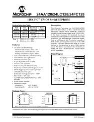
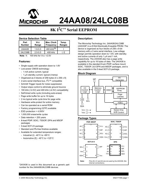
24AA08/24LC08B8K I 2 C Serial EEPROMDevice Selection TablePartNumberFeatures:VCCRangeMax. ClockFrequencyTemp.Ranges24AA08 1.8-5.5 400 kHz (1) I24LC08B 2.5-5.5 400 kHz I, ENote 1: 100 kHz for VCC 200 years• 8-lead PDIP, SOIC, TSSOP, DFN and MSOPpackages• 5-lead SOT-23 package• Standard and Pb-free finishes available• Available for extended temperature ranges:- Industrial (I): -40°C to +85°C- Automotive (E): -40°C to +125°CDescription:The Microchip Technology Inc. 24AA08/24LC08B(24XX08*) is a 8 Kbit Electrically Erasable PROM. Thedevice is organized as four blocks of 256 x 8-bitmemory with a 2-wire serial interface. Low-voltagedesign permits operation down to 1.8V, with standbyand active currents of only 1 μA and 1 mA,respectively. The 24XX08 also has a page writecapability for up to 16 bytes of data. The 24XX08 isavailable in the standard 8-pin PDIP, surface mountSOIC, TSSOP, 2x3 DFN and MSOP packages, and isalso available in the 5-lead SOT-23 package.Block DiagramI/OControlLogicI/OSDAVCCVSSSCLWPPackage TypesA0A1A2VSS1234PDIP, MSOPSOT-23-5MemoryControlLogic8765VCCWPSCLA0A1A2SDA VSSXDECHVGeneratorEEPROMArrayPageLatchesYDECSense Amp.R/W ControlSOIC, TSSOP1234DFN8765VCCWPSCLSDASCLVssSDA1 523 4WPVccA0 1A1 2A2 3VSS 48765VCCWPSCLSDA*24XX08 is used in this document as a generic partnumber for the 24AA08/24LC08B devices.Note:Pins A0, A1 and A2 are not used by the 24XX08. (Nointernal connections).© 2005 Microchip Technology Inc. DS21710E-page 1
24AA08/24LC08B1.0 ELECTRICAL CHARACTERISTICSAbsolute Maximum Ratings (†)VCC.............................................................................................................................................................................6.5VAll inputs and outputs w.r.t. VSS ......................................................................................................... -0.3V to VCC +1.0VStorage temperature ...............................................................................................................................-65°C to +150°CAmbient temperature with power applied................................................................................................-65°C to +125°CESD protection on all pins ......................................................................................................................................................≥ 4kV† NOTICE: Stresses above those listed under “Absolute Maximum Ratings” may cause permanent damage tothe device. This is a stress rating only and functional operation of the device at those or any other conditionsabove those indicated in the operational listings of this specification is not implied. Exposure to maximum ratingconditions for extended periods may affect device reliability.TABLE 1-1:DC CHARACTERISTICSVCC = +1.8V to +5.5VDC CHARACTERISTICSIndustrial (I): TA = -40°C to +85°CAutomotive (E): TA = -40°C to +125°CParam.No.Symbol Characteristic Min. Typ. Max. Units ConditionsD1 VIH WP, SCL and SDA pins — — — — —D2 — High-level input voltage 0.7 VCC — — V —D3 VIL Low-level input voltage — — 0.3 VCC V —D4 VHYS Hysteresis of Schmitt 0.05 VCC — — V (Note)Trigger inputsD5 VOL Low-level output voltage — — 0.40 V IOL = 3.0 mA, VCC = 2.5VD6 ILI Input leakage current — — ±1 μA VIN = .1V to VCCD7 ILO Output leakage current — — ±1 μA VOUT = .1V to VCCD8 CIN,COUTPin capacitance(all inputs/outputs)— — 10 pF VCC = 5.0V (Note)TA = 25°C, FCLK = 1 MHzD9 ICC write Operating current — 0.1 3 mA VCC = 5.5V, SCL = 400 kHzD10 ICC read — 0.05 1 mA —D11 ICCS Standby current ——Note:0.01—This parameter is periodically sampled and not 100% tested.15μAμAIndustrialAutomotiveSDA = SCL = VCCWP = VSSDS21710E-page 2© 2005 Microchip Technology Inc.
24AA08/24LC08BTABLE 1-2:AC CHARACTERISTICSAC CHARACTERISTICSParam.No.1 FCLK Clock frequency ——2 THIGH Clock high time 60040003 TLOW Clock low time 13004700VCC = +1.8V to +5.5VIndustrial (I): TA = -40°C to +85°CAutomotive (E): TA = -40°C to +125°CSymbol Characteristic Min. Typ. Max. Units Conditions4 TR SDA and SCL rise time(Note 1)——————————5 TF SDA and SCL fall time — ——6 THD:STA Start condition hold time 60040007 TSU:STA Start condition setuptime6004700————8 THD:DAT Data input hold time 0 ——9 TSU:DAT Data input setup time 10025010 TSU:STO Stop condition setuptime11 TAA Output valid from clock(Note 2)12 TBUF Bus free time: Time thebus must be free beforea new transmission canstart13 TOF Output fall time from VIHminimum to VILmaximum14 TSP Input filter spikesuppression(SDA and SCL pins)6004000——1300470020+0.1CB———————————400100————3001000kHz 2.5V ≤ VCC ≤ 5.5V1.8V ≤ VCC < 2.5V (24AA08)ns 2.5V ≤ VCC ≤ 5.5V1.8V ≤ VCC < 2.5V (24AA08)ns 2.5V ≤ VCC ≤ 5.5V1.8V ≤ VCC < 2.5V (24AA08)ns 2.5V ≤ VCC ≤ 5.5V (Note 1)1.8V ≤ VCC < 2.5V (24AA08)(Note 1)300 ns (Note 1)————ns 2.5V ≤ VCC ≤ 5.5V1.8V ≤ VCC < 2.5V (24AA08)ns 2.5V ≤ VCC ≤ 5.5V1.8V ≤ VCC < 2.5V (24AA08)— ns (Note 2)————9003500——250250ns 2.5V ≤ VCC ≤ 5.5V1.8V ≤ VCC < 2.5V (24AA08)ns 2.5V ≤ VCC ≤ 5.5V1.8V ≤ VCC < 2.5V (24AA08)ns 2.5V ≤ VCC ≤ 5.5V1.8V ≤ VCC < 2.5V (24AA08)ns 2.5V ≤ VCC ≤ 5.5V1.8V ≤ VCC < 2.5V (24AA08)ns 2.5V ≤ VCC ≤ 5.5V1.8V ≤ VCC < 2.5V (24AA08)— — 50 ns (Notes 1 and 3)15 TWC Write cycle time (byte or — — 5 ms —page)16 — Endurance 1M — — cycles 25°C, (Note 4)Note 1: Not 100% tested. CB = total capacitance of one bus line in pF.2: As a transmitter, the device must provide an internal minimum delay time to bridge the undefined region(minimum 300 ns) of the falling edge of SCL to avoid unintended generation of Start or Stop conditions.3: The combined TSP and VHYS specifications are due to new Schmitt Trigger inputs which provide improvednoise spike suppression. This eliminates the need for a TI specification for standard operation.4: This parameter is not tested but ensured by characterization. For endurance estimates in a specificapplication, please consult the Total Endurance Model which can be obtained from Microchip’s web siteat www.microchip.com.© 2005 Microchip Technology Inc. DS21710E-page 3
24AA08/24LC08BFIGURE 1-1:BUS TIMING DATASCLSDAIN14765328 9 104SDAOUT1112FIGURE 1-2:BUS TIMING START/STOPD4SCL7610SDAStartStopDS21710E-page 4© 2005 Microchip Technology Inc.
24AA08/24LC08B2.0 FUNCTIONAL DESCRIPTIONThe 24XX08 supports a bidirectional, 2-wire bus anddata transmission protocol. A device that sends dataonto the bus is defined as a transmitter, while a devicereceiving data is defined as a receiver. The bus has tobe controlled by a master device which generates theSerial Clock (SCL), controls the bus access andgenerates the Start and Stop conditions, while the24XX08 works as slave. Both master and slave canoperate as transmitter or receiver, but the masterdevice determines which mode is activated.3.0 BUS CHARACTERISTICSThe following bus protocol has been defined:• Data transfer may be initiated only when the busis not busy.• During data transfer, the data line must remainstable whenever the clock line is high. Changes inthe data line while the clock line is high will beinterpreted as a Start or Stop condition.Accordingly, the following bus conditions have beendefined (Figure 3-1).3.1 Bus Not Busy (A)Both data and clock lines remain high.3.2 Start Data Transfer (B)A high-to-low transition of the SDA line while the clock(SCL) is high determines a Start condition. Allcommands must be preceded by a Start condition.3.3 Stop Data Transfer (C)A low-to-high transition of the SDA line while the clock(SCL) is high determines a Stop condition. Alloperations must be ended with a Stop condition.3.4 Data Valid (D)The state of the data line represents valid data when,after a Start condition, the data line is stable for theduration of the high period of the clock signal.The data on the line must be changed during the lowperiod of the clock signal. There is one clock pulse perbit of data.Each data transfer is initiated with a Start condition andterminated with a Stop condition. The number of thedata bytes transferred between the Start and Stopconditions is determined by the master device and istheoretically unlimited, although only the last sixteenwill be stored when doing a write operation. When anoverwrite does occur it will replace data in a first-in firstout(FIFO) fashion.3.5 AcknowledgeEach receiving device, when addressed, is obliged togenerate an acknowledge after the reception of eachbyte. The master device must generate an extra clockpulse which is associated with this Acknowledge bit.Note:The 24XX08 does not generate anyAcknowledge bits if an internal programmingcycle is in progress.The device that acknowledges, has to pull down theSDA line during the acknowledge clock pulse in such away that the SDA line is stable low during the highperiod of the acknowledge related clock pulse. Ofcourse, setup and hold times must be taken intoaccount. During reads, a master must signal an end ofdata to the slave by not generating an Acknowledge biton the last byte that has been clocked out of the slave.In this case, the slave (24XX08) will leave the data linehigh to enable the master to generate the Stopcondition.FIGURE 3-1:DATA TRANSFER SEQUENCE ON THE SERIAL BUSSCL(A) (B) (D) (D) (C) (A)SDAStartConditionAddress orAcknowledgeValidDataAllowedto ChangeStopCondition© 2005 Microchip Technology Inc. DS21710E-page 5
24AA08/24LC08B3.6 Device AddressingA control byte is the first byte received following theStart condition from the master device (Figure 3-2).The control byte consists of a four-bit control code. Forthe 24XX08, this is set as ‘1010’ binary for read andwrite operations. The next three bits of the control byteare the block-select bits (B2, B1, B0). B2 is a “don’tcare” for the 24XX08. They are used by the masterdevice to select which of the four 256 word-blocks ofmemory are to be accessed. These bits are in effect thethree Most Significant bits of the word address.The last bit of the control byte defines the operation tobe performed. When set to ‘1’ a read operation isselected. When set to ‘0’ a write operation is selected.Following the Start condition, the 24XX08 monitors theSDA bus, checking the device type identifier beingtransmitted and, upon receiving a ‘1010’ code, theslave device outputs an Acknowledge signal on theSDA line. Depending on the state of the R/W bit, the24XX08 will select a read or write operation.FIGURE 3-2:SStart BitCONTROL BYTEALLOCATION1 0 1 0 x B1 B0 R/W ACKx = “don’t care”Control CodeSlave AddressBlockSelectBitsRead/Write BitAcknowledge BitOperationControlCodeBlock SelectR/WRead 1010 Block Address 1Write 1010 Block Address 0DS21710E-page 6© 2005 Microchip Technology Inc.
24AA08/24LC08B5.0 ACKNOWLEDGE POLLINGSince the device will not acknowledge during a writecycle, this can be used to determine when the cycle iscomplete (this feature can be used to maximize busthroughput). Once the Stop condition for a Writecommand has been issued from the master, the deviceinitiates the internally-timed write cycle and ACK pollingcan then be initiated immediately. This involves themaster sending a Start condition followed by the controlbyte for a Write command (R/W = 0). If the device is stillbusy with the write cycle, no ACK will be returned. If thecycle is complete, the device will return the ACK andthe master can then proceed with the next Read orWrite command. See Figure 5-1 for a flow diagram ofthis operation.6.0 WRITE PROTECTIONThe WP pin allows the user to write-protect the entirearray (000-3FF) when the pin is tied to VCC. If the pin istied to VSS the write protection is disabled.FIGURE 5-1:ACKNOWLEDGE POLLINGFLOWSendWrite CommandSend StopCondition toInitiate Write CycleSend StartSend Control Bytewith R/W = 0Did DeviceAcknowledge(ACK = 0)?NoYesNextOperationDS21710E-page 8© 2005 Microchip Technology Inc.
24AA08/24LC08BFIGURE 7-2:RANDOM READBus ActivityMasterSDA LineBus ActivitySST Control Word T ControlARByte Address (n)ARByteTTS 1 010XB1B00 S 1 0 1 0 XB1B01x = “don’t care”BlockSelectBitsACKACKBlockSelectBitsACKData (n)NoACKSTOPPFIGURE 7-3:SEQUENTIAL READBus ActivityMasterControlByteData (n) Data (n + 1) Data (n + 2) Data (n + X)STOPSDA LineBus Activity1ACKACKACKACKNoAPCKDS21710E-page 10© 2005 Microchip Technology Inc.
24AA08/24LC08B8.0 PIN DESCRIPTIONSThe descriptions of the pins are listed in Table 8-1.TABLE 8-1:PIN FUNCTION TABLEName PDIP SOIC TSSOP DFN MSOP SOT-23 DescriptionA0 1 1 1 1 1 — Not ConnectedA1 2 2 2 2 2 — Not ConnectedA2 3 3 3 3 3 — Not ConnectedVSS 4 4 4 4 4 2 GroundSDA 5 5 5 5 5 3 Serial Address/Data I/OSCL 6 6 6 6 6 1 Serial ClockWP 7 7 7 7 7 5 Write-Protect InputVCC 8 8 8 8 8 4 +1.8V to 5.5V Power Supply8.1 Serial Address/Data Input/Output(SDA)SDA is a bidirectional pin used to transfer addressesand data into and out of the device. Since it is an opendrainterminal, the SDA bus requires a pull-up resistorto VCC (typical 10 kΩ for 100 kHz, 2 kΩ for 400 kHz).For normal data transfer, SDA is allowed to changeonly during SCL low. Changes during SCL high arereserved for indicating Start and Stop conditions.8.2 Serial Clock (SCL)The SCL input is used to synchronize the data transferto and from the device.8.3 Write-Protect (WP)The WP pin must be connected to either VSS or VCC.If tied to VSS, normal memory operation is enabled(read/write the entire memory 000-03FF).If tied to VCC, write operations are inhibited. The entirememory will be write-protected. Read operations arenot affected.This feature allows the user to use the 24XX08 as aserial ROM when WP is enabled (tied to VCC).8.4 A0, A1, A2The A0, A1 and A2 pins are not used by the 24XX08.They may be left floating or tied to either VSS or VCC.© 2005 Microchip Technology Inc. DS21710E-page 11
24AA08/24LC08B9.0 PACKAGING INFORMATION9.1 Package Marking Information8-Lead PDIP (300 mil)XXXXXXXXT/XXXNNNYYWWExample:24LC08BI/P e3 13F05278-Lead SOIC (150 mil)XXXXXXXXT/XXYYWWNNNExample:24LC08BISN e3 052713F8-Lead TSSOPXXXXTYWWNNNExample:4L08I52713F8-Lead MSOPXXXXXTYWWNNNExample:4L18BI52713F5-Lead SOT-23Example:XXNNM43F8-Lead 2x3 DFNExample:XXXYWWNN24452713DS21710E-page 12© 2005 Microchip Technology Inc.
24AA08/24LC08B1st Line MarkingSOT-23DFNPart No. TSSOP MSOPI-Temp E-Temp I-Temp E-Temp24AA08 4A08 4A08T B4NN — 241 —24LC08B 4L08 4L2BT M4NN N4NN 244 —Legend: XX...X Part number or part number codeT Temperature (I, E)Y Year code (last digit of calendar year)YY Year code (last 2 digits of calendar year)WW Week code (week of January 1 is week ‘01’)NNNe3Alphanumeric traceability code (2 characters for small packages)Pb-free JEDEC designator for Matte Tin (Sn)Note:Note:For very small packages with no room for the Pb-free JEDEC designatore3 , the marking will only appear on the outer carton or reel label.In the event the full Microchip part number cannot be marked on one line, it willbe carried over to the next line, thus limiting the number of availablecharacters for customer-specific information.Note:Please visit www.microchip.com/Pbfree for the latest information on Pb-free conversion.*Standard OTP marking consists of Microchip part number, year code, week code, and traceability code.© 2005 Microchip Technology Inc. DS21710E-page 13
24AA08/24LC08B8-Lead Plastic Dual In-line (P) – 300 mil (PDIP)E12Dn1αEAA2cA1LβeBB1BpUnits INCHES* MILLIMETERSDimension Limits MIN NOM MAX MIN NOM MAXNumber of Pins n 8 8Pitch p .100 2.54Top to Seating Plane A .140 .155 .170 3.56 3.94 4.32Molded Package Thickness A2 .115 .130 .145 2.92 3.30 3.68Base to Seating Plane A1 .015 0.38Shoulder to Shoulder Width E .300 .313 .325 7.62 7.94 8.26Molded Package Width E1 .240 .250 .260 6.10 6.35 6.60Overall Length D .360 .373 .385 9.14 9.46 9.78Tip to Seating Plane L .125 .130 .135 3.18 3.30 3.43Lead Thickness c .008 .012 .015 0.20 0.29 0.38Upper Lead Width B1 .045 .058 .070 1.14 1.46 1.78Lower Lead Width B .014 .018 .022 0.36 0.46 0.56Overall Row Spacing § eB .310 .370 .430 7.87 9.40 10.92Mold Draft Angle Top α 5 10 15 5 10 15Mold Draft Angle Bottom β 5 10 15 5 10 15* Controlling Parameter§ Significant CharacteristicNotes:Dimensions D and E1 do not include mold flash or protrusions. Mold flash or protrusions shall not exceed.010” (0.254mm) per side.JEDEC Equivalent: MS-001Drawing No. C04-018DS21710E-page 14© 2005 Microchip Technology Inc.
24AA08/24LC08B8-Lead Plastic Small Outline (SN) – Narrow, 150 mil (SOIC)EE1p2DBn145°hαcAA2φβLA1UnitsINCHES*MILLIMETERSDimension Limits MIN NOM MAX MIN NOM MAXNumber of Pinsn88Pitchp.0501.27Overall HeightA .053 .061 .069 1.35 1.55 1.75Molded Package Thickness A2 .052 .056 .061 1.32 1.42 1.55Standoff §A1 .004 .007 .010 0.10 0.18 0.25Overall WidthE .228 .237 .244 5.79 6.02 6.20Molded Package WidthE1 .146 .154 .157 3.71 3.91 3.99Overall LengthD .189 .193 .197 4.80 4.90 5.00Chamfer Distanceh .010 .015 .020 0.25 0.38 0.51Foot LengthL .019 .025 .030 0.48 0.62 0.76Foot Angle φ 0 4 8 0 4 8Lead Thicknessc .008 .009 .010 0.20 0.23 0.25Lead WidthB .013 .017 .020 0.33 0.42 0.51Mold Draft Angle Topα0 12 150 12 15Mold Draft Angle Bottomβ0 12 150 12 15* Controlling Parameter§ Significant CharacteristicNotes:Dimensions D and E1 do not include mold flash or protrusions. Mold flash or protrusions shall not exceed.010” (0.254mm) per side.JEDEC Equivalent: MS-012Drawing No. C04-057© 2005 Microchip Technology Inc. DS21710E-page 15
24AA08/24LC08B8-Lead Plastic Thin Shrink Small Outline (ST) – 4.4 mm (TSSOP)EE1p2DBn1AαcφA1A2βLUnitsINCHESMILLIMETERS*Dimension Limits MIN NOM MAX MIN NOM MAXNumber of Pinsn88Pitchp.0260.65Overall HeightA.0431.10Molded Package Thickness A2 .033 .035 .037 0.85 0.90 0.95Standoff §A1 .002 .004 .006 0.05 0.10 0.15Overall WidthE .246 .251 .256 6.25 6.38 6.50Molded Package WidthE1 .169 .173 .177 4.30 4.40 4.50Molded Package LengthD .114 .118 .122 2.90 3.00 3.10Foot LengthL .020 .024 .028 0.50 0.60 0.70Foot Angle φ 0 4 8 0 4 8Lead Thicknessc .004 .006 .008 0.09 0.15 0.20Lead WidthB .007 .010 .012 0.19 0.25 0.30Mold Draft Angle Topα05 1005 10Mold Draft Angle Bottomβ05 1005 10* Controlling Parameter§ Significant CharacteristicNotes:Dimensions D and E1 do not include mold flash or protrusions. Mold flash or protrusions shall not exceed.005” (0.127mm) per side.JEDEC Equivalent: MO-153Drawing No. C04-086DS21710E-page 16© 2005 Microchip Technology Inc.
24AA08/24LC08B8-Lead Plastic Micro Small Outline Package (MS) (MSOP)EE1pBn 12DαcφAA1A2β(F)LUnitsINCHESMILLIMETERS*Dimension Limits MIN NOM MAX MIN NOMNumber of Pinsn88Pitchp.026 BSC0.65 BSCOverall HeightA-- .043- -Molded Package Thickness A2 .030 .033 .037 0.75 0.85StandoffA1 .000- .006 0.00-Overall WidthE.193 TYP.4.90 BSCMolded Package WidthE1.118 BSC3.00 BSCOverall LengthD.118 BSC3.00 BSCFoot LengthL .016 .024 .031 0.40 0.60Footprint (Reference)Foot AngleFφ0°.037 REF- 8° 0°0.95 REF-Lead Thicknessc .003 .006 .009 0.08-Lead WidthB .009 .012 .016 0.22-Mold Draft Angle Topα5°- 15° 5° -Mold Draft Angle Bottomβ5° - 15° 5° -*Controlling ParameterNotes:Dimensions D and E1 do not include mold flash or protrusions. Mold flash or protrusions shall notexceed .010" (0.254mm) per side.JEDEC Equivalent: MO-187Drawing No. C04-111MAX1.100.950.150.808°0.230.4015°15°© 2005 Microchip Technology Inc. DS21710E-page 17
24AA08/24LC08B5-Lead Plastic Small Outline Transistor (OT) (SOT-23)EE1pBp1Dn1αcAA2βLφA1UnitsDimension LimitsNumber of PinsnPitchpOutside lead pitch (basic)p1Overall HeightAMolded Package Thickness A2Standoff §A1Overall WidthEMolded Package WidthE1Overall LengthDFoot LengthLFoot AngleφLead ThicknesscLead WidthBMold Draft Angle TopαMold Draft Angle Bottomβ* Controlling Parameter§ Significant CharacteristicMIN.035.035.000.102.059.110.0140.004.01400INCHES*NOM5.038.075.046.043.003.110.064.116.0185.006.01755MAX.057.051.006.118.069.122.02210.008.0201010MILLIMETERSMIN NOM50.951.900.90 1.180.90 1.100.00 0.082.60 2.801.50 1.632.80 2.950.35 0.45050.09 0.150.35 0.430505Notes:Dimensions D and E1 do not include mold flash or protrusions. Mold flash or protrusions shall not exceed.010” (0.254mm) per side.JEDEC Equivalent: MO-178Drawing No. C04-091MAX1.451.300.153.001.753.100.55100.200.501010DS21710E-page 18© 2005 Microchip Technology Inc.
24AA08/24LC08B8-Lead Plastic Dual Flat No Lead Package (MC) 2x3x0.9 mm Body (DFN) – Saw SingulatedpDbnLEE2PIN 1ID INDEXAREA(NOTE 2)TOP VIEWEXPOSEDMETALPADD22 1BOTTOM VIEWA3A1AEXPOSEDTIE BAR(NOTE 1)UnitsINCHESMILLIMETERS*Dimension LimitsMIN NOM MAX MIN NOMNumber of Pinsn88Pitchp.020 BSC0.50 BSCOverall HeightA.031 .035 .039 0.80 0.90StandoffA1.000 .001 .002 0.00 0.02Contact ThicknessA3.008 REF.0.20 REF.Overall LengthD.079 BSC2.00 BSCExposed Pad LengthOverall WidthD2E.055--.118 BSC.064 1.39--3.00 BSCExposed Pad WidthE2.047-- .071 1.20--Contact Widthb.008 .010 .012 0.20 0.25Contact Length*Controlling ParameterL.012 .016 .020 0.30 0.40Notes:1. Package may have one or more exposed tie bars at ends.2. Pin 1 visual index feature may vary, but must be located within the hatched area.3. Exposed pad dimensions vary with paddle size.4. JEDEC equivalent: MO-229Drawing No. C04-123(Note 3)(Note 3)Revised 05/24/04MAX1.000.051.621.800.300.50© 2005 Microchip Technology Inc. DS21710E-page 19
24AA08/24LC08BAPPENDIX A:REVISION HISTORYRevision CCorrections to Section 1.0, Electrical Characteristics.Section 9.1, 24LC08B standard marking code.Revision DAdded DFN package.Revision ERevised Figure 3-1: Control Byte Allocation; Figure 4-1Byte Write; Figure 4-2 Page Write; Section 6.0 WriteProtection; Figure 7-1 Current Address Read; Figure 7-2 Random Read; Figure 7-3 Sequential Read; 8.3Write-Protect (000-3FF).DS21710E-page 20© 2005 Microchip Technology Inc.
24AA08/24LC08BTHE MICROCHIP WEB SITEMicrochip provides online support via our WWW site atwww.microchip.com. This web site is used as a meansto make files and information easily available tocustomers. Accessible by using your favorite Internetbrowser, the web site contains the followinginformation:• Product Support – Data sheets and errata,application notes and sample programs, designresources, user’s guides and hardware supportdocuments, latest software releases and archivedsoftware• General Technical Support – Frequently AskedQuestions (FAQ), technical support requests,online discussion groups, Microchip consultantprogram member listing• Business of Microchip – Product selector andordering guides, latest Microchip press releases,listing of seminars and events, listings ofMicrochip sales offices, distributors and factoryrepresentativesCUSTOMER SUPPORTUsers of Microchip products can receive assistancethrough several channels:• Distributor or Representative• Local Sales Office• Field Application Engineer (FAE)• Technical Support• Development Systems Information LineCustomers should contact their distributor,representative or field application engineer (FAE) forsupport. Local sales offices are also available to helpcustomers. A listing of sales offices and locations isincluded in the back of this document.Technical support is available through the web siteat: http://support.microchip.comCUSTOMER CHANGE NOTIFICATIONSERVICEMicrochip’s customer notification service helps keepcustomers current on Microchip products. Subscriberswill receive e-mail notification whenever there arechanges, updates, revisions or errata related to aspecified product family or development tool of interest.To register, access the Microchip web site atwww.microchip.com, click on Customer ChangeNotification and follow the registration instructions.© 2005 Microchip Technology Inc. DS21710E-page 21
24AA08/24LC08BREADER RESPONSEIt is our intention to provide you with the best documentation possible to ensure successful use of your Microchip product.If you wish to provide your comments on organization, clarity, subject matter, and ways in which our documentationcan better serve you, please FAX your comments to the Technical Publications Manager at (480) 792-4150.Please list the following information, and use this outline to provide us with your comments about this document.To:RE:Technical Publications ManagerReader ResponseTotal Pages Sent ________From: NameCompanyAddressCity / State / ZIP / CountryTelephone: (_______) _________ - _________Application (optional):Would you like a reply? Y NFAX: (______) _________ - _________Device:24AA08/24LC08BLiterature Number:DS21710EQuestions:1. What are the best features of this document?2. How does this document meet your hardware and software development needs?3. Do you find the organization of this document easy to follow? If not, why?4. What additions to the document do you think would enhance the structure and subject?5. What deletions from the document could be made without affecting the overall usefulness?6. Is there any incorrect or misleading information (what and where)?7. How would you improve this document?DS21710E-page 22© 2005 Microchip Technology Inc.
24AA08/24LC08BPRODUCT IDENTIFICATION SYSTEMTo order or obtain information, e.g., on pricing or delivery, refer to the factory or the listed sales office.PART NO. X /XXDeviceTemperatureRange:TemperatureRangePackage24AA08: = 1.8V, 16 Kbit I 2 C Serial EEPROM24AA08T: = 1.8V, 16 Kbit I 2 C Serial EEPROM(Tape and Reel)24LC08B: = 2.5V, 16 Kbit I 2 C Serial EEPROM24LC08BT: = 2.5V, 16 Kbit I 2 C Serial EEPROM(Tape and Reel)IE= -40°C to +85°C= -40°C to +125°CPackage: P = Plastic DIP (300 mil body), 8-leadSN = Plastic SOIC (150 mil body), 8-leadST = Plastic TSSOP (4.4 mm), 8-leadMC = 2x3 DFN, 8-leadMS = Plastic Micro Small Outline (MSOP), 8-leadOT = SOT-23, 5-lead (Tape and Reel only)Lead Finish: Blank = Standard 63% / 37% SnPbG = Matte Tin (Pure Sn)XLead FinishExamples:a) 24AA08-I/P: Industrial Temperature,1.8V,PDIP packageb) 24AA08-I/SN: Industrial Temperature,1.8V,SOIC packagec) 24AA08T-I/OT: Industrial Temperature,1.8V, SOT-23 package, Tape and Reeld) 24LC08B-I/P: Industrial Temperature, 2.5V,PDIP packagee) 24LC08B-E/SN: Automotive Temp.,2.5VSOIC packagef) 24LC08BT-I/OT: Industrial Temperature,2.5V, SOT-23 package, Tape and Reelg) 24LC08B-I/PG: Industrial Temperature,2.5V, PDIP package, Pb-freeh) 24LC08BT-I/SNG: Industrial Temperature,2.5V, SOIC package, Tape and Reel,Pb-freeSales and SupportData SheetsProducts supported by a preliminary Data Sheet may have an errata sheet describing minor operational differences andrecommended workarounds. To determine if an errata sheet exists for a particular device, please contact one of the following:1. Your local Microchip sales office2. The Microchip Corporate Literature Center U.S. FAX: (480) 792-72773. The Microchip Worldwide Site (www.microchip.com)Please specify which device, revision of silicon and Data Sheet (include Literature #) you are using.New Customer Notification SystemRegister on our web site (www.microchip.com/cn) to receive the most current information on our products.© 2005 Microchip Technology Inc. DS21710E-page 23
24AA08/24LC08BNOTES:DS21710E-page 24© 2005 Microchip Technology Inc.
Note the following details of the code protection feature on Microchip devices:• Microchip products meet the specification contained in their particular Microchip Data Sheet.• Microchip believes that its family of products is one of the most secure families of its kind on the market today, when used in theintended manner and under normal conditions.• There are dishonest and possibly illegal methods used to breach the code protection feature. All of these methods, to ourknowledge, require using the Microchip products in a manner outside the operating specifications contained in Microchip’s DataSheets. Most likely, the person doing so is engaged in theft of intellectual property.• Microchip is willing to work with the customer who is concerned about the integrity of their code.• Neither Microchip nor any other semiconductor manufacturer can guarantee the security of their code. Code protection does notmean that we are guaranteeing the product as “unbreakable.”Code protection is constantly evolving. We at Microchip are committed to continuously improving the code protection features of ourproducts. Attempts to break Microchip’s code protection feature may be a violation of the Digital Millennium Copyright Act. If such actsallow unauthorized access to your software or other copyrighted work, you may have a right to sue for relief under that Act.Information contained in this publication regarding deviceapplications and the like is provided only for your convenienceand may be superseded by updates. It is your responsibility toensure that your application meets with your specifications.MICROCHIP MAKES NO REPRESENTATIONS OR WAR-RANTIES OF ANY KIND WHETHER EXPRESS OR IMPLIED,WRITTEN OR ORAL, STATUTORY OR OTHERWISE,RELATED TO THE INFORMATION, INCLUDING BUT NOTLIMITED TO ITS CONDITION, QUALITY, PERFORMANCE,MERCHANTABILITY OR FITNESS FOR PURPOSE.Microchip disclaims all liability arising from this information andits use. Use of Microchip’s products as critical components inlife support systems is not authorized except with expresswritten approval by Microchip. No licenses are conveyed,implicitly or otherwise, under any Microchip intellectual propertyrights.TrademarksThe Microchip name and logo, the Microchip logo, Accuron,dsPIC, KEELOQ, microID, MPLAB, PIC, PICmicro, PICSTART,PRO MATE, PowerSmart, rfPIC, and SmartShunt areregistered trademarks of Microchip Technology Incorporatedin the U.S.A. and other countries.AmpLab, FilterLab, Migratable Memory, MXDEV, MXLAB,PICMASTER, SEEVAL, SmartSensor and The EmbeddedControl Solutions Company are registered trademarks ofMicrochip Technology Incorporated in the U.S.A.Analog-for-the-Digital Age, Application Maestro, dsPICDEM,dsPICDEM.net, dsPICworks, ECAN, ECONOMONITOR,FanSense, FlexROM, fuzzyLAB, In-Circuit SerialProgramming, ICSP, ICEPIC, Linear Active Thermistor,MPASM, MPLIB, MPLINK, MPSIM, PICkit, PICDEM,PICDEM.net, PICLAB, PICtail, PowerCal, PowerInfo,PowerMate, PowerTool, rfLAB, rfPICDEM, Select Mode,Smart Serial, SmartTel, Total Endurance and WiperLock aretrademarks of Microchip Technology Incorporated in theU.S.A. and other countries.SQTP is a service mark of Microchip Technology Incorporatedin the U.S.A.All other trademarks mentioned herein are property of theirrespective companies.© 2005, Microchip Technology Incorporated, Printed in theU.S.A., All Rights Reserved.Printed on recycled paper.Microchip received ISO/TS-16949:2002 quality system certification forits worldwide headquarters, design and wafer fabrication facilities inChandler and Tempe, Arizona and Mountain View, California inOctober 2003. The Company’s quality system processes andprocedures are for its PICmicro ® 8-bit MCUs, KEELOQ ® code hoppingdevices, Serial EEPROMs, microperipherals, nonvolatile memory andanalog products. In addition, Microchip’s quality system for the designand manufacture of development systems is ISO 9001:2000 certified.© 2005 Microchip Technology Inc. DS21710E-page 25
WORLDWIDE SALES AND SERVICEAMERICASCorporate Office2355 West Chandler Blvd.Chandler, AZ 85224-6199Tel: 480-792-7200Fax: 480-792-7277Technical Support:http://support.microchip.comWeb Address:www.microchip.comAtlantaAlpharetta, GATel: 770-640-0034Fax: 770-640-0307BostonWestborough, MATel: 774-760-0087Fax: 774-760-0088ChicagoItasca, ILTel: 630-285-0071Fax: 630-285-0075DallasAddison, TXTel: 972-818-7423Fax: 972-818-2924DetroitFarmington Hills, MITel: 248-538-2250Fax: 248-538-2260KokomoKokomo, INTel: 765-864-8360Fax: 765-864-8387Los AngelesMission Viejo, CATel: 949-462-9523Fax: 949-462-9608San JoseMountain View, CATel: 650-215-1444Fax: 650-961-0286TorontoMississauga, Ontario,CanadaTel: 905-673-0699Fax: 905-673-6509ASIA/PACIFICAustralia - SydneyTel: 61-2-9868-6733Fax: 61-2-9868-6755China - BeijingTel: 86-10-8528-2100Fax: 86-10-8528-2104China - ChengduTel: 86-28-8676-6200Fax: 86-28-8676-6599China - FuzhouTel: 86-591-8750-3506Fax: 86-591-8750-3521China - Hong Kong SARTel: 852-2401-1200Fax: 852-2401-3431China - QingdaoTel: 86-532-8502-7355Fax: 86-532-8502-7205China - ShanghaiTel: 86-21-5407-5533Fax: 86-21-5407-5066China - ShenyangTel: 86-24-2334-2829Fax: 86-24-2334-2393China - ShenzhenTel: 86-755-8203-2660Fax: 86-755-8203-1760China - ShundeTel: 86-757-2839-5507Fax: 86-757-2839-5571China - WuhanTel: 86-27-5980-5300Fax: 86-27-5980-5118China - XianTel: 86-29-8833-7250Fax: 86-29-8833-7256ASIA/PACIFICIndia - BangaloreTel: 91-80-2229-0061Fax: 91-80-2229-0062India - New DelhiTel: 91-11-5160-8631Fax: 91-11-5160-8632India - PuneTel: 91-20-2566-1512Fax: 91-20-2566-1513Japan - YokohamaTel: 81-45-471- 6166Fax: 81-45-471-6122Korea - GumiTel: 82-54-473-4301Fax: 82-54-473-4302Korea - SeoulTel: 82-2-554-7200Fax: 82-2-558-5932 or82-2-558-5934Malaysia - PenangTel: 604-646-8870Fax: 604-646-5086Philippines - ManilaTel: 632-634-9065Fax: 632-634-9069SingaporeTel: 65-6334-8870Fax: 65-6334-8850Taiwan - Hsin ChuTel: 886-3-572-9526Fax: 886-3-572-6459Taiwan - KaohsiungTel: 886-7-536-4818Fax: 886-7-536-4803Taiwan - TaipeiTel: 886-2-2500-6610Fax: 886-2-2508-0102Thailand - BangkokTel: 66-2-694-1351Fax: 66-2-694-1350EUROPEAustria - WeisTel: 43-7242-2244-399Fax: 43-7242-2244-393Denmark - CopenhagenTel: 45-4450-2828Fax: 45-4485-2829France - ParisTel: 33-1-69-53-63-20Fax: 33-1-69-30-90-79Germany - MunichTel: 49-89-627-144-0Fax: 49-89-627-144-44Italy - MilanTel: 39-0331-742611Fax: 39-0331-466781Netherlands - DrunenTel: 31-416-690399Fax: 31-416-690340Spain - MadridTel: 34-91-352-30-52Fax: 34-91-352-11-47UK - WokinghamTel: 44-118-921-5869Fax: 44-118-921-582008/24/05DS21710E-page 26© 2005 Microchip Technology Inc.