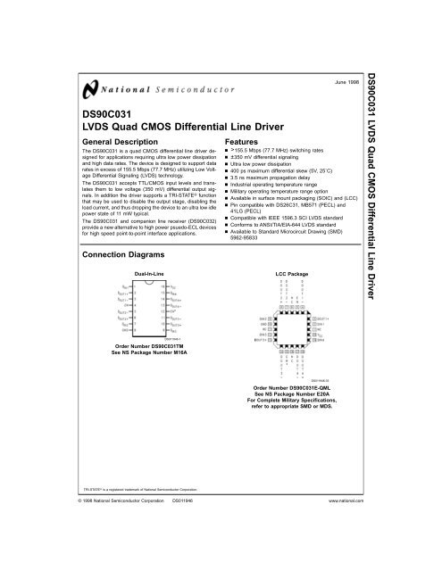
DS90C031 LVDS Quad CMOS Differential Line Driver
DS90C031 LVDS Quad CMOS Differential Line Driver
DS90C031 LVDS Quad CMOS Differential Line Driver

Create successful ePaper yourself
Turn your PDF publications into a flip-book with our unique Google optimized e-Paper software.
<strong>DS90C031</strong><br />
<strong>LVDS</strong> <strong>Quad</strong> <strong>CMOS</strong> <strong>Differential</strong> <strong>Line</strong> <strong>Driver</strong><br />
General Description<br />
The <strong>DS90C031</strong> is a quad <strong>CMOS</strong> differential line driver designed<br />
for applications requiring ultra low power dissipation<br />
and high data rates. The device is designed to support data<br />
rates in excess of 155.5 Mbps (77.7 MHz) utilizing Low Voltage<br />
<strong>Differential</strong> Signaling (<strong>LVDS</strong>) technology.<br />
The <strong>DS90C031</strong> accepts TTL/<strong>CMOS</strong> input levels and translates<br />
them to low voltage (350 mV) differential output signals.<br />
In addition the driver supports a TRI-STATE ® function<br />
that may be used to disable the output stage, disabling the<br />
load current, and thus dropping the device to an ultra low idle<br />
power state of 11 mW typical.<br />
The <strong>DS90C031</strong> and companion line receiver (DS90C032)<br />
provide a new alternative to high power psuedo-ECL devices<br />
for high speed point-to-point interface applications.<br />
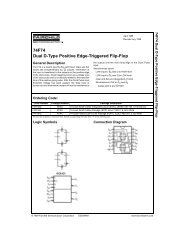
Connection Diagrams<br />
Dual-In-<strong>Line</strong><br />
Features<br />
n >155.5 Mbps (77.7 MHz) switching rates<br />
n ±350 mV differential signaling<br />
n Ultra low power dissipation<br />
n 400 ps maximum differential skew (5V, 25˚C)<br />
n 3.5 ns maximum propagation delay<br />
n Industrial operating temperature range<br />
n Military operating temperature range option<br />
n Available in surface mount packaging (SOIC) and (LCC)<br />
n Pin compatible with DS26C31, MB571 (PECL) and<br />
41LG (PECL)<br />
n Compatible with IEEE 1596.3 SCI <strong>LVDS</strong> standard<br />
n Conforms to ANSI/TIA/EIA-644 <strong>LVDS</strong> standard<br />
n Available to Standard Microcircuit Drawing (SMD)<br />
5962-95833<br />
LCC Package<br />
June 1998<br />
<strong>DS90C031</strong> <strong>LVDS</strong> <strong>Quad</strong> <strong>CMOS</strong> <strong>Differential</strong> <strong>Line</strong> <strong>Driver</strong><br />
DS011946-1<br />
Order Number <strong>DS90C031</strong>TM<br />
See NS Package Number M16A<br />
DS011946-33<br />
Order Number <strong>DS90C031</strong>E-QML<br />
See NS Package Number E20A<br />
For Complete Military Specifications,<br />
refer to appropriate SMD or MDS.<br />
TRI-STATE ® is a registered trademark of National Semiconductor Corporation.<br />
© 1998 National Semiconductor Corporation DS011946 www.national.com
Functional Diagram<br />
DS011946-2<br />
Truth Table<br />
DRIVER<br />
Enables Input Outputs<br />
EN EN* D IN D OUT+ D OUT−<br />
L H X Z Z<br />
All other combinations L L H<br />
of ENABLE inputs H H L<br />
www.national.com 2
Absolute Maximum Ratings (Note 1)<br />
If Military/Aerospace specified devices are required,<br />
please contact the National Semiconductor Sales Office/<br />
Distributors for availability and specifications.<br />
Supply Voltage (V CC ) −0.3V to +6V<br />
Input Voltage (D IN )<br />
−0.3V to (V CC + 0.3V)<br />
Enable Input Voltage (EN, EN*) −0.3V to (V CC + 0.3V)<br />
Output Voltage (D OUT+ ,D OUT− ) −0.3V to (V CC + 0.3V)<br />
Short Circuit Duration<br />
(D OUT+ ,D OUT− ) Continuous<br />
Maximum Package Power Dissipation @ +25˚C<br />
M Package<br />
1068 mW<br />
E Package<br />
1900 mW<br />
Derate M Package<br />
8.5 mW/˚C above +25˚C<br />
Derate E Package<br />
12.8 mW/˚C above +25˚C<br />
Storage Temperature Range<br />
−65˚C to +150˚C<br />
Lead Temperature Range<br />
Soldering (4 sec.)<br />
+260˚C<br />
Maximum Junction Temperature<br />
(<strong>DS90C031</strong>T)<br />
+150˚C<br />
Maximum Junction Temperature<br />
(<strong>DS90C031</strong>E)<br />
+175˚C<br />
ESD Rating (Note 7)<br />
(HBM, 1.5 kΩ, 100 pF) ≥ 3,500V<br />
(EIAJ, 0 Ω, 200 pF)<br />
≥ 250V<br />
Recommended Operating<br />
Conditions<br />
Min Typ Max Units<br />
Supply Voltage (V CC ) +4.5 +5.0 +5.5 V<br />
Operating Free Air Temperature (T A )<br />
<strong>DS90C031</strong>T −40 +25 +85 ˚C<br />
<strong>DS90C031</strong>E −55 +25 +125 ˚C<br />
Electrical Characteristics<br />
Over supply voltage and operating temperature ranges, unless otherwise specified. (Notes 2, 3)<br />
Symbol Parameter Conditions Pin Min Typ Max Units<br />
V OD1 <strong>Differential</strong> Output Voltage R L = 100Ω (Figure 1) D OUT− , 250 345 450 mV<br />
∆V OD1 Change in Magnitude of V OD1<br />
for Complementary Output<br />
States<br />
D OUT+ 4 35 |mV|<br />
V OS Offset Voltage 1.125 1.25 1.375 V<br />
∆V OS<br />
Change in Magnitude of V OS for<br />
5 25 |mV|<br />
Complementary Output States<br />
V OH Output Voltage High R L = 100Ω 1.41 1.60 V<br />
V OL Output Voltage Low 0.90 1.07 V<br />
V IH Input Voltage High D IN , 2.0 V CC V<br />
V IL Input Voltage Low EN, GND 0.8 V<br />
I I Input Current V IN =V CC , GND, 2.5V or 0.4V<br />
EN*<br />
−10 ±1 +10 µA<br />
V CL Input Clamp Voltage I CL = −18 mA −1.5 −0.8 V<br />
I OS Output Short Circuit Current V OUT = 0V (Note 8) D OUT− ,<br />
−3.5 −5.0 mA<br />
I OZ Output TRI-STATE Current EN = 0.8V and EN* = 2.0V,<br />
D OUT+ −10 ±1 +10 µA<br />
V OUT =0VorV CC<br />
I CC No Load Supply Current D IN =V CC or GND <strong>DS90C031</strong>T V CC 1.7 3.0 mA<br />
<strong>Driver</strong>s Enabled<br />
D IN = 2.5V or 0.4V 4.0 6.5 mA<br />
I CCL<br />
I CCZ<br />
Loaded Supply Current<br />
<strong>Driver</strong>s Enabled<br />
No Load Supply Current<br />
<strong>Driver</strong>s Disabled<br />
R L = 100Ω All Channels<br />
V IN =V CC or GND<br />
(all inputs)<br />
Switching Characteristics<br />
V CC = +5.0V, T A = +25˚C <strong>DS90C031</strong>T. (Notes 3, 4, 6, 9)<br />
<strong>DS90C031</strong>T 15.4 21.0 mA<br />
<strong>DS90C031</strong>E 15.4 25.0 mA<br />
D IN =V CC or GND<br />
<strong>DS90C031</strong>T 2.2 4.0 mA<br />
EN = GND, EN* = V CC <strong>DS90C031</strong>E 2.2 10.0 mA<br />
Symbol Parameter Conditions Min Typ Max Units<br />
t PHLD <strong>Differential</strong> Propagation Delay High to Low R L = 100Ω, C L =5pF 1.0 2.0 3.0 ns<br />
t PLHD <strong>Differential</strong> Propagation Delay Low to High (Figure 2 and Figure 3) 1.0 2.1 3.0 ns<br />
t SKD <strong>Differential</strong> Skew |t PHLD –t PLHD | 0 80 400 ps<br />
t SK1 Channel-to-Channel Skew (Note 4) 0 300 600 ps<br />
3<br />
www.national.com
Switching Characteristics (Continued)<br />
V CC = +5.0V, T A = +25˚C <strong>DS90C031</strong>T. (Notes 3, 4, 6, 9)<br />
Symbol Parameter Conditions Min Typ Max Units<br />
t TLH Rise Time 0.35 1.5 ns<br />
t THL Fall Time 0.35 1.5 ns<br />
t PHZ Disable Time High to Z R L = 100Ω,<br />
2.5 10 ns<br />
t PLZ Disable Time Low to Z C L =5pF<br />
2.5 10 ns<br />
t PZH Enable Time Z to High<br />
(Figure 4 and Figure 5)<br />
2.5 10 ns<br />
t PZL Enable Time Z to Low 2.5 10 ns<br />
Switching Characteristics<br />
V CC = +5.0V ± 10%, T A = −40˚C to +85˚C <strong>DS90C031</strong>T. (Notes 3, 4, 5, 6, 9)<br />
Symbol Parameter Conditions Min Typ Max Units<br />
t PHLD <strong>Differential</strong> Propagation Delay High to Low R L = 100Ω, C L =5pF 0.5 2.0 3.5 ns<br />
t PLHD <strong>Differential</strong> Propagation Delay Low to High (Figure 2 and Figure 3) 0.5 2.1 3.5 ns<br />
t SKD <strong>Differential</strong> Skew |t PHLD –t PLHD | 0 80 900 ps<br />
t SK1 Channel-to-Channel Skew (Note 4) 0 0.3 1.0 ns<br />
t SK2 Chip to Chip Skew (Note 5) 3.0 ns<br />
t TLH Rise Time 0.35 2.0 ns<br />
t THL Fall Time 0.35 2.0 ns<br />
t PHZ Disable Time High to Z R L = 100Ω,<br />
2.5 15 ns<br />
t PLZ Disable Time Low to Z C L =5pF<br />
2.5 15 ns<br />
t PZH Enable Time Z to High<br />
(Figure 4 and Figure 5)<br />
2.5 15 ns<br />
t PZL Enable Time Z to Low 2.5 15 ns<br />
Switching Characteristics<br />
V CC = +5.0V ± 10%, T A = −55˚C to +125˚C <strong>DS90C031</strong>E. (Notes 3, 4, 5, 6, 9, 10)<br />
Symbol Parameter Conditions Min Typ Max Units<br />
t PHLD <strong>Differential</strong> Propagation Delay High to Low R L = 100Ω, C L =20pF 0.5 2.0 5.0 ns<br />
t PLHD <strong>Differential</strong> Propagation Delay Low to High (Figure 3)<br />
0.5 2.1 5.0 ns<br />
t<br />
C L Connected between<br />
SKD <strong>Differential</strong> Skew |t PHLD –t PLHD | 0 0.08 3.0 ns<br />
each Output and GND<br />
t SK1 Channel-to-Channel Skew (Note 4) 0 0.3 3.0 ns<br />
t SK2 Chip to Chip Skew (Note 5) 4.5 ns<br />
t PHZ Disable Time High to Z R L = 100Ω,<br />
2.5 20 ns<br />
t PLZ Disable Time Low to Z C L =5pF<br />
2.5 20 ns<br />
t PZH Enable Time Z to High<br />
(Figure 4 and Figure 5)<br />
2.5 20 ns<br />
t PZL Enable Time Z to Low 2.5 20 ns<br />
Parameter Measurement Information<br />
FIGURE 1. <strong>Driver</strong> V OD and V OS Test Circuit<br />
DS011946-3<br />
www.national.com 4
Parameter Measurement Information (Continued)<br />
DS011946-4<br />
FIGURE 2. <strong>Driver</strong> Propagation Delay and Transition Time Test Circuit<br />
FIGURE 3. <strong>Driver</strong> Propagation Delay and Transition Time Waveforms<br />
DS011946-5<br />
FIGURE 4. <strong>Driver</strong> TRI-STATE Delay Test Circuit<br />
DS011946-6<br />
5<br />
www.national.com
Parameter Measurement Information (Continued)<br />
Typical Application<br />
FIGURE 5. <strong>Driver</strong> TRI-STATE Delay Waveform<br />
DS011946-7<br />
Applications Information<br />
FIGURE 6. Point-to-Point Application<br />
DS011946-8<br />
<strong>LVDS</strong> drivers and receivers are intended to be primarily used<br />
in an uncomplicated point-to-point configuration as is shown<br />
in Figure 6. This configuration provides a clean signaling environment<br />
for the quick edge rates of the drivers. The receiver<br />
is connected to the driver through a balanced media<br />
which may be a standard twisted pair cable, a parallel pair<br />
cable, or simply PCB traces. Typically, the characteristic impedance<br />
of the media is in the range of 100Ω. A termination<br />
resistor of 100Ω should be selected to match the media, and<br />
is located as close to the receiver input pins as possible. The<br />
termination resistor converts the current sourced by the<br />
driver into a voltage that is detected by the receiver. Other<br />
configurations are possible such as a multi-receiver configuration,<br />
but the effects of a mid-stream connector(s), cable<br />
stub(s), and other impedance discontinuities as well as<br />
ground shifting, noise margin limits, and total termination<br />
loading must be taken into account.<br />
The <strong>DS90C031</strong> differential line driver is a balanced current<br />
source design. A current mode driver, generally speaking<br />
has a high output impedance and supplies a constant current<br />
for a range of loads (a voltage mode driver on the other<br />
hand supplies a constant voltage for a range of loads). Current<br />
is switched through the load in one direction to produce<br />
a logic state and in the other direction to produce the other<br />
logic state. The typical output current is mere 3.4 mA, a minimum<br />
of 2.5 mA, and a maximum of 4.5 mA. The current<br />
mode requires (as discussed above) that a resistive termination<br />
be employed to terminate the signal and to complete<br />
the loop as shown in Figure 6. AC or unterminated configurations<br />
are not allowed. The 3.4 mA loop current will develop<br />
a differential voltage of 340 mV across the 100Ω termination<br />
resistor which the receiver detects with a 240 mV minimum<br />
differential noise margin neglecting resistive line losses<br />
(driven signal minus receiver threshold (340 mV – 100 mV =<br />
240 mV)). The signal is centered around +1.2V (<strong>Driver</strong> Offset,<br />
V OS ) with respect to ground as shown inFigure 7. Note<br />
that the steady-state voltage (V SS ) peak-to-peak swing is<br />
twice the differential voltage (V OD ) and is typically 680 mV.<br />
The current mode driver provides substantial benefits over<br />
voltage mode drivers, such as an RS-422 driver. Its quiescent<br />
current remains relatively flat versus switching frequency.<br />
Whereas the RS-422 voltage mode driver increases<br />
exponentially in most case between 20 MHz–50 MHz. This<br />
is due to the overlap current that flows between the rails of<br />
the device when the internal gates switch. Whereas the current<br />
mode driver switches a fixed current between its output<br />
without any substantial overlap current. This is similar to<br />
some ECL and PECL devices, but without the heavy static<br />
I CC requirements of the ECL/PECL designs. <strong>LVDS</strong> requires<br />
80% less current than similar PECL devices. AC specifications<br />
for the driver are a tenfold improvement over other existing<br />
RS-422 drivers.<br />
The TRI-STATE function allows the driver outputs to be disabled,<br />
thus obtaining an even lower power state when the<br />
transmission of data is not required.<br />
www.national.com 6
Applications Information (Continued)<br />
The footprint of the <strong>DS90C031</strong> is the same as the industry<br />
standard 26LS31 <strong>Quad</strong> <strong>Differential</strong> (RS-422) <strong>Driver</strong>.<br />
FIGURE 7. <strong>Driver</strong> Output Levels<br />
DS011946-9<br />
Pin Descriptions<br />
Pin No. Name Description<br />
(SOIC)<br />
1, 7,<br />
9, 15<br />
2, 6,<br />
10, 14<br />
3, 5,<br />
11, 13<br />
D IN<br />
D OUT+<br />
D OUT−<br />
<strong>Driver</strong> input pin, TTL/<strong>CMOS</strong><br />
compatible<br />
Non-inverting driver output pin,<br />
<strong>LVDS</strong> levels<br />
Inverting driver output pin,<br />
<strong>LVDS</strong> levels<br />
4 EN Active high enable pin, OR-ed<br />
with EN*<br />
12 EN* Active low enable pin, OR-ed<br />
with EN<br />
Pin No. Name Description<br />
(SOIC)<br />
16 V CC Power supply pin, +5V ± 10%<br />
8 GND Ground pin<br />
Ordering Information<br />
Operating Package Type/ Order Number<br />
Temperature Number<br />
−40˚C to +85˚C SOP/M16A <strong>DS90C031</strong>TM<br />
−55˚C to +125˚C LCC/E20A <strong>DS90C031</strong>E-QML<br />
<strong>DS90C031</strong>E-QML (NSID)<br />
5962-95833 (SMD)<br />
Note 1: “Absolute Maximum Ratings” are those values beyond which the safety of the device cannot be guaranteed. They are not meant to imply that the devices<br />
should be operated at these limits. The table of “Electrical Characteristics” specifies conditions of device operation.<br />
Note 2: Current into device pins is defined as positive. Current out of device pins is defined as negative. All voltages are referenced to ground except: V OD1 and<br />
∆V OD1 .<br />
Note 3: All typicals are given for: V CC = +5.0V, T A = +25˚C.<br />
Note 4: Channel-to-Channel Skew is defined as the difference between the propagation delay of the channel and the other channels in the same chip with an event<br />
on the inputs.<br />
Note 5: Chip to Chip Skew is defined as the difference between the minimum and maximum specified differential propagation delays.<br />
Note 6: Generator waveform for all tests unless otherwise specified: f=1MHz, Z O =50Ω,t r ≤6 ns, and t f ≤ 6 ns.<br />
Note 7: ESD Ratings:<br />
HBM (1.5 kΩ, 100 pF) ≥ 3,500V<br />
EIAJ (0Ω, 200 pF) ≥ 250V<br />
Note 8: Output short circuit current (I OS ) is specified as magnitude only, minus sign indicates direction only.<br />
Note 9: C L includes probe and jig capacitance.<br />
Note 10: Guaranteed by characterization data (<strong>DS90C031</strong>E).<br />
7<br />
www.national.com
Typical Performance Characteristics<br />
Power Supply Current<br />
vs Power Supply Voltage<br />
Power Supply Current<br />
vs Temperature<br />
DS011946-10<br />
DS011946-11<br />
Power Supply Current<br />
vs Power Supply Voltage<br />
Power Supply Current<br />
vs Temperature<br />
DS011946-12<br />
DS011946-13<br />
Output TRI-STATE Current<br />
vs Power Supply Voltage<br />
Output Short Circuit Current<br />
vs Power Supply Voltage<br />
DS011946-14<br />
DS011946-15<br />
www.national.com 8
Typical Performance Characteristics (Continued)<br />
<strong>Differential</strong> Output Voltage<br />
vs Power Supply Voltage<br />
<strong>Differential</strong> Output Voltage<br />
vs Ambient Temperature<br />
DS011946-16<br />
DS011946-17<br />
Output Voltage High vs<br />
Power Supply Voltage<br />
Output Voltage High vs<br />
Ambient Temperature<br />
DS011946-18<br />
DS011946-19<br />
Output Voltage Low vs<br />
Power Supply Voltage<br />
Output Voltage Low vs<br />
Ambient Temperature<br />
DS011946-20<br />
DS011946-21<br />
9<br />
www.national.com
Typical Performance Characteristics (Continued)<br />
Offset Voltage vs<br />
Power Supply Voltage<br />
Offset Voltage vs<br />
Ambient Temperature<br />
DS011946-22<br />
DS011946-23<br />
Power Supply Current<br />
vs Frequency<br />
Power Supply Current<br />
vs Frequency<br />
DS011946-24<br />
DS011946-25<br />
<strong>Differential</strong> Output Voltage<br />
vs Load Resistor<br />
<strong>Differential</strong> Propagation Delay<br />
vs Power Supply Voltage<br />
DS011946-26<br />
DS011946-27<br />
www.national.com 10
Typical Performance Characteristics (Continued)<br />
<strong>Differential</strong> Propagation Delay<br />
vs Ambient Temperature<br />
<strong>Differential</strong> Skew vs<br />
Power Supply Voltage<br />
DS011946-29<br />
DS011946-28<br />
<strong>Differential</strong> Skew vs<br />
Ambient Temperature<br />
<strong>Differential</strong> Transition Time<br />
vs Power Supply Voltage<br />
DS011946-30<br />
DS011946-31<br />
<strong>Differential</strong> Transition Time<br />
vs Ambient Temperature<br />
DS011946-32<br />
11<br />
www.national.com
Physical Dimensions inches (millimeters) unless otherwise noted<br />
20-Lead Ceramic Leadless Chip Carrier, Type C<br />
Order Number <strong>DS90C031</strong>E-QML<br />
NS Package Number E20A<br />
16-Lead (0.150" Wide) Molded Small Outline Package, JEDEC<br />
Order Number <strong>DS90C031</strong>TM<br />
NS Package Number M16A<br />
13<br />
www.national.com
<strong>DS90C031</strong> <strong>LVDS</strong> <strong>Quad</strong> <strong>CMOS</strong> <strong>Differential</strong> <strong>Line</strong> <strong>Driver</strong><br />
LIFE SUPPORT POLICY<br />
NATIONAL’S PRODUCTS ARE NOT AUTHORIZED FOR USE AS CRITICAL COMPONENTS IN LIFE SUPPORT DE-<br />
VICES OR SYSTEMS WITHOUT THE EXPRESS WRITTEN APPROVAL OF THE PRESIDENT OF NATIONAL SEMI-<br />
CONDUCTOR CORPORATION. As used herein:<br />
1. Life support devices or systems are devices or systems<br />
which, (a) are intended for surgical implant into<br />
the body, or (b) support or sustain life, and whose failure<br />
to perform when properly used in accordance<br />
with instructions for use provided in the labeling, can<br />
be reasonably expected to result in a significant injury<br />
to the user.<br />
2. A critical component in any component of a life support<br />
device or system whose failure to perform can be reasonably<br />
expected to cause the failure of the life support<br />
device or system, or to affect its safety or effectiveness.<br />
National Semiconductor<br />
Corporation<br />
Americas<br />
Tel: 1-800-272-9959<br />
Fax: 1-800-737-7018<br />
Email: support@nsc.com<br />
www.national.com<br />
National Semiconductor<br />
Europe<br />
Fax: +49 (0) 1 80-530 85 86<br />
Email: europe.support@nsc.com<br />
Deutsch Tel: +49 (0) 1 80-530 85 85<br />
English Tel: +49 (0) 1 80-532 78 32<br />
Français Tel: +49 (0) 1 80-532 93 58<br />
Italiano Tel: +49 (0) 1 80-534 16 80<br />
National Semiconductor<br />
Asia Pacific Customer<br />
Response Group<br />
Tel: 65-2544466<br />
Fax: 65-2504466<br />
Email: sea.support@nsc.com<br />
National Semiconductor<br />
Japan Ltd.<br />
Tel: 81-3-5620-6175<br />
Fax: 81-3-5620-6179<br />
National does not assume any responsibility for use of any circuitry described, no circuit patent licenses are implied and National reserves the right at any time without notice to change said circuitry and specifications.