Xilinx XC95108 In-System Programmable CPLD datasheet, v3.0 (12 ...
Xilinx XC95108 In-System Programmable CPLD datasheet, v3.0 (12 ...
Xilinx XC95108 In-System Programmable CPLD datasheet, v3.0 (12 ...
- No tags were found...

Create successful ePaper yourself
Turn your PDF publications into a flip-book with our unique Google optimized e-Paper software.
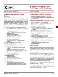
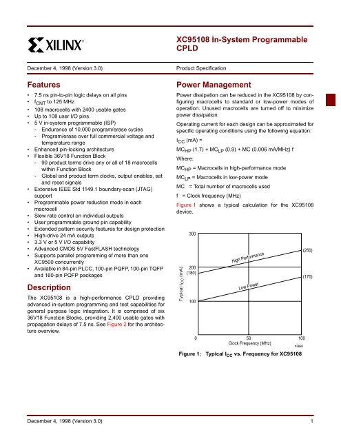
®1<strong>XC95108</strong> <strong>In</strong>-<strong>System</strong> <strong>Programmable</strong><strong>CPLD</strong>December 4, 1998 (Version 3.0) 1 1* Product SpecificationFeatures• 7.5 ns pin-to-pin logic delays on all pins• f CNT to <strong>12</strong>5 MHz• 108 macrocells with 2400 usable gates• Up to 108 user I/O pins• 5 V in-system programmable (ISP)- Endurance of 10,000 program/erase cycles- Program/erase over full commercial voltage andtemperature range• Enhanced pin-locking architecture• Flexible 36V18 Function Block- 90 product terms drive any or all of 18 macrocellswithin Function Block- Global and product term clocks, output enables, setand reset signals• Extensive IEEE Std 1149.1 boundary-scan (JTAG)support• <strong>Programmable</strong> power reduction mode in eachmacrocell• Slew rate control on individual outputs• User programmable ground pin capability• Extended pattern security features for design protection• High-drive 24 mA outputs• 3.3 V or 5 V I/O capability• Advanced CMOS 5V FastFLASH technology• Supports parallel programming of more than oneXC9500 concurrently• Available in 84-pin PLCC, 100-pin PQFP, 100-pin TQFPand 160-pin PQFP packagesDescriptionThe <strong>XC95108</strong> is a high-performance <strong>CPLD</strong> providingadvanced in-system programming and test capabilities forgeneral purpose logic integration. It is comprised of six36V18 Function Blocks, providing 2,400 usable gates withpropagation delays of 7.5 ns. See Figure 2 for the architectureoverview.Power ManagementPower dissipation can be reduced in the <strong>XC95108</strong> by configuringmacrocells to standard or low-power modes ofoperation. Unused macrocells are turned off to minimizepower dissipation.Operating current for each design can be approximated forspecific operating conditions using the following equation:I CC (mA) =MC HP (1.7) + MC LP (0.9) + MC (0.006 mA/MHz) fWhere:MC HP = Macrocells in high-performance modeMC LP = Macrocells in low-power modeMC = Total number of macrocells usedf = Clock frequency (MHz)Figure 1 shows a typical calculation for the <strong>XC95108</strong>device.Typical I CC (mA)300200(180)100High PerformanceLow Power0 50Clock Frequency (MHz)100X5898Figure 1: Typical I CC vs. Frequency for <strong>XC95108</strong>(250)(170)December 4, 1998 (Version 3.0) 1
<strong>XC95108</strong> <strong>In</strong>-<strong>System</strong> <strong>Programmable</strong> <strong>CPLD</strong>JTAG Port13JTAGController<strong>In</strong>-<strong>System</strong> Programming ControllerI/OI/O1836FunctionBlock 1Macrocells1 to 18I/OI/OI/OI/OI/OI/OI/O/GCKI/O/GSRI/O/GTS3<strong>12</strong>I/OBlocksFastCONNECT Switch Matrix181818363636FunctionBlock 2Macrocells1 to 18FunctionBlock 3Macrocells1 to 18FunctionBlock 4Macrocells1 to 181836FunctionBlock 5Macrocells1 to 181836FunctionBlock 6Macrocells1 to 18Figure 2: <strong>XC95108</strong> ArchitectureX5897Note: Function Block outputs (indicated by the bold line) drive the I/O Blocks directly2 December 4, 1998 (Version 3.0)
<strong>XC95108</strong> <strong>In</strong>-<strong>System</strong> <strong>Programmable</strong> <strong>CPLD</strong>DC Characteristics Over Recommended Operating ConditionsSymbol Parameter Test Conditions Min Max UnitsV OH Output high voltage for 5 V operation I OH = -4.0 mA2.4 VV CC = MinOutput high voltage for 3.3 V operationI OH = -3.2 mAVV CC = Min 2.4V OL Output low voltage for 5 V operation I OL = 24 mA0.5 VV CC = MinOutput low voltage for 3.3 V operationI OL = 10 mA0.4 VV CC = MinI IL <strong>In</strong>put leakage current V CC = Max±10.0 µAV IN = GND or V CCI IH I/O high-Z leakage current V CC = Max±10.0 µAV IN = GND or V CCC IN I/O capacitance V IN = GND10.0 pFf = 1.0 MHzI CC Operating Supply Current(low power mode, active)V I = GND, No loadf = 1.0 MHz100 (Typ) maAC CharacteristicsSymbolParameter<strong>XC95108</strong>-7 <strong>XC95108</strong>-10 <strong>XC95108</strong>-15 <strong>XC95108</strong>-20UnitsMin Max Min Max Min Max Min Maxt PD I/O to output valid 7.5 10.0 15.0 20.0 nst SU I/O setup time before GCK 4.5 6.0 8.0 10.0 nst H I/O hold time after GCK 0.0 0.0 0.0 0.0 nst CO GCK to output valid 4.5 6.0 8.0 10.0 ns1f CNT 16-bit counter frequency <strong>12</strong>5.0 111.1 95.2 83.3 MHz2f SYSTEM Multiple FB internal operating frequency 83.3 66.7 55.6 50.0 MHzt PSU I/O setup time before p-term clock input 0.5 2.0 4.0 4.0 nst PH I/O hold time after p-term clock input 4.0 4.0 4.0 6.0 nst PCO P-term clock to output valid 8.5 10.0 <strong>12</strong>.0 16.0 nst OE GTS to output valid 5.5 6.0 11.0 16.0 nst OD GTS to output disable 5.5 6.0 11.0 16.0 nst POE Product term OE to output enabled 9.5 10.0 14.0 18.0 nst POD Product term OE to output disabled 9.5 10.0 14.0 18.0 nst WLH GCK pulse width (High or Low) 4.0 4.5 5.5 5.5 nsNote: 1. f CNT is the fastest 16-bit counter frequency available, using the local feedback when applicable.f CNT is also the Export Control Maximum flip-flop toggle rate, f TOG .2. f SYSTEM is the internal operating frequency for general purpose system designs spanning multiple FBs.4 December 4, 1998 (Version 3.0)
<strong>XC95108</strong> <strong>In</strong>-<strong>System</strong> <strong>Programmable</strong> <strong>CPLD</strong>V TESTDevice OutputR 1Output TypeV CCIO5.0 V3.3 VV TEST5.0 V3.3 VR 1160 Ω260 ΩR 2<strong>12</strong>0 Ω360 ΩC L35 pF35 pFR 2C LX5906Figure 3: AC Load Circuit<strong>In</strong>ternal Timing ParametersSymbolParameterNote: 3. t PTA is multiplied by the span of the function as defined in the family data sheet.<strong>XC95108</strong>-7 <strong>XC95108</strong>-10 <strong>XC95108</strong>-15 <strong>XC95108</strong>-20UnitsMin Max Min Max Min Max Min MaxBuffer Delayst IN <strong>In</strong>put buffer delay 2.5 3.5 4.5 6.5 nst GCK GCK buffer delay 1.5 2.5 3.0 3.0 nst GSR GSR buffer delay 4.5 6.0 7.5 9.5 nst GTS GTS buffer delay 5.5 6.0 11.0 16.0 nst OUT Output buffer delay 2.5 3.0 4.5 6.5 nst EN Output buffer enable/disable delay 0.0 0.0 0.0 0.0 nsProduct Term Control Delayst PTCK Product term clock delay 3.0 3.0 2.5 2.5 nst PTSR Product term set/reset delay 2.0 2.5 3.0 3.0 nst PTTS Product term 3-state delay 4.5 3.5 5.0 5.0 ns<strong>In</strong>ternal Register and Combinatorial delayst PDI Combinatorial logic propagation delay 0.5 1.0 3.0 4.0 nst SUI Register setup time 1.5 2.5 3.5 3.5 nst HI Register hold time 3.0 3.5 4.5 6.5 nst COI Register clock to output valid time 0.5 0.5 0.5 0.5 nst AOI Register async. S/R to output delay 6.5 7.0 8.0 8.0 nst RAI Register async. S/R recovery before clock 7.5 10.0 10.0 10.0 nst LOGI <strong>In</strong>ternal logic delay 2.0 2.5 3.0 3.0 nst LOGILP <strong>In</strong>ternal low power logic delay 10.0 11.0 11.5 11.5 nsFeedback Delayst F FastCONNECT matrix feedback delay 8.0 9.5 11.0 13.0 nst LF Function Block local feeback delay 4.0 3.5 3.5 5.0 nsTime Adders3t PTA <strong>In</strong>cremental Product Term Allocator delay 1.0 1.0 1.0 1.5 nst SLEW Slew-rate limited delay 4.0 4.5 5.0 5.5 nsDecember 4, 1998 (Version 3.0) 5
<strong>XC95108</strong> <strong>In</strong>-<strong>System</strong> <strong>Programmable</strong> <strong>CPLD</strong><strong>XC95108</strong> I/O PinsFunctionBlockMacrocell PC84 PQ100 TQ100 PQ160 BScanOrderNotes: [1] Global control pinNotesFunctionBlockBScanMacrocell PC84 PQ100 TQ100 PQ160Order Notes1 1 – – – 25 321 3 1 – – – 45 2131 2 1 15 13 21 318 3 2 14 31 29 47 2101 3 2 16 14 22 315 3 3 15 32 30 49 2071 4 – 21 19 29 3<strong>12</strong> 3 4 – 36 34 57 2041 5 3 17 15 23 309 3 5 17 34 32 54 2011 6 4 18 16 24 306 3 6 18 35 33 56 1981 7 – – – 27 303 3 7 – – – 50 1951 8 5 19 17 26 300 3 8 19 37 35 58 1921 9 6 20 18 28 297 3 9 20 38 36 59 1891 10 – 26 24 36 294 3 10 – 45 43 69 1861 11 7 22 20 30 291 3 11 21 39 37 60 1831 <strong>12</strong> 9 24 22 33 288 [1] 3 <strong>12</strong> 23 41 39 62 1801 13 – – – 34 285 3 13 – – – 52 1771 14 10 25 23 35 282 [1] 3 14 24 42 40 63 1741 15 11 27 25 37 279 3 15 25 43 41 64 1711 16 <strong>12</strong> 29 27 42 276 [1] 3 16 26 44 42 68 1681 17 13 30 28 44 273 3 17 31 51 49 77 1651 18 – – – 43 270 3 18 – – – 74 1622 1 – – – 158 267 4 1 – – – <strong>12</strong>3 1592 2 71 98 96 154 264 4 2 57 83 81 134 1562 3 72 99 97 156 261 4 3 58 84 82 135 1532 4 – 4 2 4 258 4 4 – 82 80 133 1502 5 74 1 99 159 255 [1] 4 5 61 87 85 138 1472 6 75 3 1 2 252 4 6 62 88 86 139 1442 7 – – – 9 249 4 7 – – – <strong>12</strong>8 14<strong>12</strong> 8 76 5 3 6 246 [1] 4 8 63 89 87 140 1382 9 77 6 4 8 243 [1] 4 9 65 91 89 142 1352 10 – 9 7 <strong>12</strong> 240 4 10 – – – 147 1322 11 79 8 6 11 237 4 11 66 92 90 143 <strong>12</strong>92 <strong>12</strong> 80 10 8 13 234 4 <strong>12</strong> 67 93 91 144 <strong>12</strong>62 13 – – – 14 231 4 13 – – – 153 <strong>12</strong>32 14 81 11 9 15 228 4 14 68 95 93 146 <strong>12</strong>02 15 82 <strong>12</strong> 10 17 225 4 15 69 96 94 148 1172 16 83 13 11 18 222 4 16 – 94 92 145 1142 17 84 14 <strong>12</strong> 19 219 4 17 70 97 95 152 11<strong>12</strong> 18 – – – 16 216 4 18 – – – 155 1086 December 4, 1998 (Version 3.0)
<strong>XC95108</strong> <strong>In</strong>-<strong>System</strong> <strong>Programmable</strong> <strong>CPLD</strong><strong>XC95108</strong> I/O Pins (continued)FunctionBlockMacrocell PC84 PQ100 TQ100 PQ160 BScanOrder<strong>XC95108</strong> Global, JTAG and Power PinsNotesFunctionBlockBScanMacrocell PC84 PQ100 TQ100 PQ160Order Notes5 1 – – – 76 105 6 1 – – – 91 515 2 32 52 50 79 102 6 2 45 67 65 103 485 3 33 54 52 82 99 6 3 46 68 66 104 455 4 – 48 46 72 96 6 4 – 75 73 116 425 5 34 55 53 86 93 6 5 47 69 67 106 395 6 35 56 54 88 90 6 6 48 70 68 108 365 7 – – – 78 87 6 7 – – – 105 335 8 36 57 55 90 84 6 8 50 72 70 111 305 9 37 58 56 92 81 6 9 51 73 71 113 275 10 – – – 84 78 6 10 – – – 107 245 11 39 60 58 95 75 6 11 52 74 72 115 215 <strong>12</strong> 40 62 60 97 72 6 <strong>12</strong> 53 76 74 117 185 13 – – – 87 69 6 13 – – – 1<strong>12</strong> 155 14 41 63 61 98 66 6 14 54 78 76 <strong>12</strong>2 <strong>12</strong>5 15 43 65 63 101 63 6 15 55 79 77 <strong>12</strong>4 95 16 – 61 59 96 60 6 16 – 81 79 <strong>12</strong>9 65 17 44 66 64 102 57 6 17 56 80 78 <strong>12</strong>6 35 18 – – – 89 54 6 18 – – – 114 0Pin Type PC84 PQ100 TQ100 PQ160I/O/GCK1 9 24 22 33I/O/GCK2 10 25 23 35I/O/GCK3 <strong>12</strong> 29 27 42I/O/GTS1 76 5 3 6I/O/GTS2 77 6 4 8I/O/GSR 74 1 99 159TCK 30 50 48 75TDI 28 47 45 71TDO 59 85 83 136TMS 29 49 47 73V CCINT 5 V 38,73,78 7,59,100 5,57,98 10,46,94,157V CCIO 3.3 V/5 V 22,64 28,40,53,90 26,38,51,88 1,41,61,81,<strong>12</strong>1,141GND 8,16,27,42,49,60 2,23,33,46,64,71,77,86 100,21,31,44,62,69,75,84 20,31,40,51,70,80,99GND – – – 100,110,<strong>12</strong>0,<strong>12</strong>7,137GND – – – 160No connects – – – 3,5,7,32,38,39,48,53,55,65,66,67,83,85,93,109,118,119,<strong>12</strong>5,130,131,132,149,150,151December 4, 1998 (Version 3.0) 7
<strong>XC95108</strong> <strong>In</strong>-<strong>System</strong> <strong>Programmable</strong> <strong>CPLD</strong>Ordering <strong>In</strong>formation<strong>XC95108</strong> -7 PQ 160 CDevice TypeSpeedTemperature RangeNumber of PinsPackage TypeSpeed Options- 20 20 ns pin-to-pin delay-15 15 ns pin-to-pin delay-10 10 ns pin-to-pin delay-7 7 ns pin-to-pin delayPackaging OptionsPC84 84-Pin Plastic Leaded Chip Carrier (PLCC)PQ100 100-Pin Plastic Quad Flat Pack (PQFP)TQ100 100-Pin Very Thin Quad Flat Pack (TQFP)PQ160 160-Pin Plastic Quad Flat Pack (PQFP)Temperature OptionsC Commercial 0°C to +70°CI <strong>In</strong>dustrial –40°C to +85°CComponent AvailabilityPins 84 100 160TypeC = Commercial = 0° to +70°C I = <strong>In</strong>dustrial = –40° to +85°CRevision ControlPlasticPLCCPlasticPQFPPlasticTQFPPlasticPQFPCode PC84 PQ100 TQ100 PQ160–20 C(I) C(I) C(I) C(I)–15 C(I) C(I) C(I) C(I)<strong>XC95108</strong>–10 C(I) C(I) C(I) C(I)–7 C(I) C(I) C(I) C(I)DateRevision<strong>12</strong>/04/98 Update AC Characteristics and <strong>In</strong>ternal Parameters8 December 4, 1998 (Version 3.0)