DS90C031 LVDS Quad CMOS Differential Line Driver
DS90C031 LVDS Quad CMOS Differential Line Driver
DS90C031 LVDS Quad CMOS Differential Line Driver

You also want an ePaper? Increase the reach of your titles
YUMPU automatically turns print PDFs into web optimized ePapers that Google loves.
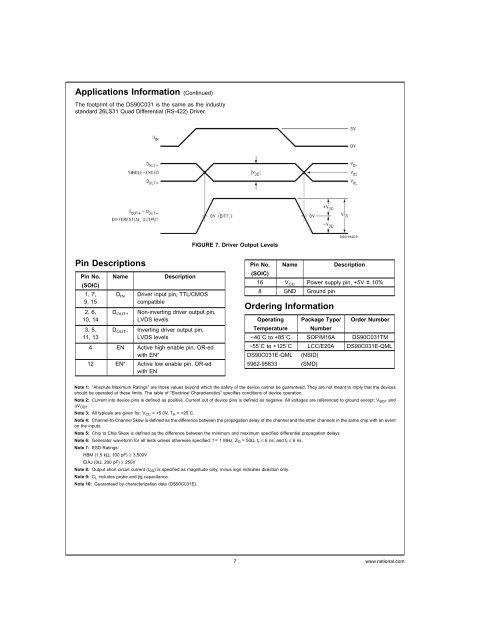
Applications Information (Continued)<br />
The footprint of the <strong>DS90C031</strong> is the same as the industry<br />
standard 26LS31 <strong>Quad</strong> <strong>Differential</strong> (RS-422) <strong>Driver</strong>.<br />
FIGURE 7. <strong>Driver</strong> Output Levels<br />
DS011946-9<br />
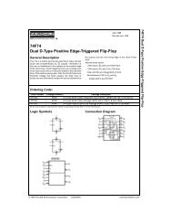
Pin Descriptions<br />
Pin No. Name Description<br />
(SOIC)<br />
1, 7,<br />
9, 15<br />
2, 6,<br />
10, 14<br />
3, 5,<br />
11, 13<br />
D IN<br />
D OUT+<br />
D OUT−<br />
<strong>Driver</strong> input pin, TTL/<strong>CMOS</strong><br />
compatible<br />
Non-inverting driver output pin,<br />
<strong>LVDS</strong> levels<br />
Inverting driver output pin,<br />
<strong>LVDS</strong> levels<br />
4 EN Active high enable pin, OR-ed<br />
with EN*<br />
12 EN* Active low enable pin, OR-ed<br />
with EN<br />
Pin No. Name Description<br />
(SOIC)<br />
16 V CC Power supply pin, +5V ± 10%<br />
8 GND Ground pin<br />
Ordering Information<br />
Operating Package Type/ Order Number<br />
Temperature Number<br />
−40˚C to +85˚C SOP/M16A <strong>DS90C031</strong>TM<br />
−55˚C to +125˚C LCC/E20A <strong>DS90C031</strong>E-QML<br />
<strong>DS90C031</strong>E-QML (NSID)<br />
5962-95833 (SMD)<br />
Note 1: “Absolute Maximum Ratings” are those values beyond which the safety of the device cannot be guaranteed. They are not meant to imply that the devices<br />
should be operated at these limits. The table of “Electrical Characteristics” specifies conditions of device operation.<br />
Note 2: Current into device pins is defined as positive. Current out of device pins is defined as negative. All voltages are referenced to ground except: V OD1 and<br />
∆V OD1 .<br />
Note 3: All typicals are given for: V CC = +5.0V, T A = +25˚C.<br />
Note 4: Channel-to-Channel Skew is defined as the difference between the propagation delay of the channel and the other channels in the same chip with an event<br />
on the inputs.<br />
Note 5: Chip to Chip Skew is defined as the difference between the minimum and maximum specified differential propagation delays.<br />
Note 6: Generator waveform for all tests unless otherwise specified: f=1MHz, Z O =50Ω,t r ≤6 ns, and t f ≤ 6 ns.<br />
Note 7: ESD Ratings:<br />
HBM (1.5 kΩ, 100 pF) ≥ 3,500V<br />
EIAJ (0Ω, 200 pF) ≥ 250V<br />
Note 8: Output short circuit current (I OS ) is specified as magnitude only, minus sign indicates direction only.<br />
Note 9: C L includes probe and jig capacitance.<br />
Note 10: Guaranteed by characterization data (<strong>DS90C031</strong>E).<br />
7<br />
www.national.com