Design of Low Cost Broadband Class-E Power Amplifier Using Low ...
Design of Low Cost Broadband Class-E Power Amplifier Using Low ...
Design of Low Cost Broadband Class-E Power Amplifier Using Low ...

Create successful ePaper yourself
Turn your PDF publications into a flip-book with our unique Google optimized e-Paper software.
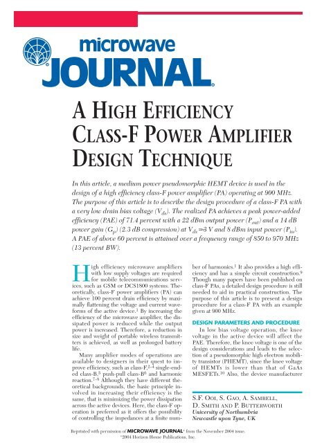
A HIGH EFFICIENCY<br />
CLASS-F POWER AMPLIFIER<br />
DESIGN TECHNIQUE<br />
In this article, a medium power pseudomorphic HEMT device is used in the<br />
design <strong>of</strong> a high efficiency class-F power amplifier (PA) operating at 900 MHz.<br />
The purpose <strong>of</strong> this article is to describe the design procedure <strong>of</strong> a class-F PA with<br />
a very low drain bias voltage (V ds ). The realized PA achieves a peak power-added<br />
efficiency (PAE) <strong>of</strong> 71.4 percent with a 22 dBm output power (P out ) and a 14 dB<br />
power gain (G p ) (2.3 dB compression) at V ds = 3 V and 8 dBm input power (P in ).<br />
A PAE <strong>of</strong> above 60 percent is attained over a frequency range <strong>of</strong> 850 to 970 MHz<br />
(13 percent BW).<br />
High efficiency microwave amplifiers<br />
with low supply voltages are required<br />
for mobile telecommunications services,<br />
such as GSM or DCS1800 systems. Theoretically,<br />
class-F power amplifiers (PA) can<br />
achieve 100 percent drain efficiency by maximally<br />
flattening the voltage and current waveforms<br />
<strong>of</strong> the active device. 1 By increasing the<br />
efficiency <strong>of</strong> the microwave amplifier, the dissipated<br />
power is reduced while the output<br />
power is increased. Therefore, a reduction in<br />
size and weight <strong>of</strong> portable wireless transmitters<br />
is achieved, as well as prolonged battery<br />
life.<br />
Many amplifier modes <strong>of</strong> operations are<br />
available to designers in their quest to improve<br />
efficiency, such as class-F, 2–4 single-ended<br />
class-B, 5 push-pull class-B 6 and harmonic<br />
reaction. 7–8 Although they have different theoretical<br />
backgrounds, the basic principle involved<br />
in increasing their efficiency is the<br />
same, that is minimizing the power dissipation<br />
across the active devices. Here, the class-F operation<br />
is preferred as it <strong>of</strong>fers the possibility<br />
<strong>of</strong> controlling the impedances at a finite num-<br />
ber <strong>of</strong> harmonics. 1 It also provides a high efficiency<br />
and has a simple circuit construction. 9<br />
Though many papers have been published on<br />
class-F PAs, a detailed design procedure is still<br />
needed to aid in practical construction. The<br />
purpose <strong>of</strong> this article is to present a design<br />
procedure for a class-F PA with an example<br />
given at 900 MHz.<br />
DESIGN PARAMETERS AND PROCEDURE<br />
In low bias voltage operation, the knee<br />
voltage in the active device will affect the<br />
PAE. Therefore, the knee voltage is one <strong>of</strong> the<br />
design considerations and leads to the selection<br />
<strong>of</strong> a pseudomorphic high electron mobility<br />
transistor (PHEMT), since the knee voltage<br />
<strong>of</strong> HEMTs is lower than that <strong>of</strong> GaAs<br />
MESFETs. 10 Also, the device manufacturer<br />
S.F. OOI, S. GAO, A. SAMBELL,<br />
D. SMITH AND P. BUTTERWORTH<br />
University <strong>of</strong> Northumbria<br />
Newcastle upon Tyne, UK<br />
Reprinted with permission <strong>of</strong> MICROWAVE JOURNAL ® from the November 2004 issue.<br />
©<br />
2004 Horizon House Publications, Inc.
TABLE I<br />
RF PARAMETERS OBTAINED<br />
FROM DC SIMULATION<br />
USING THE ADS SIMULATOR<br />
V dsmin (V) 0.7<br />
V dsmax (V) 5.5<br />
I dss @ V ds = 3V, V gs = 0V (A) 0.12<br />
I dmax @ V ds = 3V, V gs = 0.6V (A) 0.25<br />
V p @ V ds = 3V (V) –0.8<br />
Gm max @ V ds = 3V, V gs = 0V (S) 0.24<br />
supplies a large-signal device model<br />
for this active device, which allows<br />
better initial models to be built. The<br />
typically stated small-signal S-parameters<br />
and static IV curves are only<br />
applicable for small-signal levels and<br />
therefore do not provide accurate<br />
modeling <strong>of</strong> the device behavior as a<br />
PA. 11 A large-signal device model is<br />
necessary for the accurate simulation<br />
<strong>of</strong> PAs using the harmonic balance<br />
method.<br />
The important design parameters<br />
in PAs are power-added efficiency<br />
(PAE), drain efficiency (η d ) and power<br />
gain (G p ). PAE is defined as the<br />
ratio <strong>of</strong> the additional RF power provided<br />
by the amplifier to the DC<br />
power: 12<br />
PAE P out<br />
–<br />
=<br />
P<br />
P<br />
where P in is the RF input power.<br />
PAE can also be rewritten as<br />
⎛ 1 ⎞<br />
PAE = ηd<br />
1 – () 2<br />
⎝<br />
⎜ Gp<br />
⎠<br />
⎟<br />
where η d is the drain efficiency defined<br />
by<br />
Pout<br />
η d<br />
= () 3<br />
P<br />
V gs0 (t)<br />
V gs cos(ωt )<br />
dc<br />
dc<br />
V gs (t)<br />
in<br />
TECHNICAL FEATURE<br />
I d (t)<br />
I g (t)<br />
V ds (t)<br />
() 1<br />
V ds0 (t)<br />
▲ Fig. 1 The substitute generator technique.<br />
V ds1 cos(ωt + θ 1 )<br />
V ds2 cos(2ωt + θ 2 )<br />
V ds3 cos(3ωt + θ 3 )<br />
and G p is the power gain defined by<br />
The amplifier must also be evaluated<br />
for its stability condition using<br />
large signal S-parameters (LSSP)<br />
over a wide band <strong>of</strong> frequencies. This<br />
measurement gives the distance from<br />
the center <strong>of</strong> the Smith chart to the<br />
nearest output (load) stability circle.<br />
This stability factor is given by 13<br />
µ=<br />
G<br />
p<br />
Pout<br />
= () 4<br />
P<br />
1 – S<br />
2<br />
11<br />
S – S ∆ + S S<br />
22 11 12 21<br />
() 5<br />
where ∆ is the determinant <strong>of</strong> the<br />
scattering matrix.<br />
If µ > 1, the device is unconditionally<br />
stable. This single parameter can<br />
replace the dual Rollet (K > 1) and<br />
auxiliary conditions for determining<br />
unconditional stability. It is noticed<br />
that the active device alone is unstable<br />
over almost the entire frequency<br />
range (low frequency to f max ) due to<br />
its high transconductance. Therefore,<br />
a stabilizing circuit is required to<br />
make sure the circuit is unconditionally<br />
stable from low frequency to f max .<br />
The design starts with DC simulation,<br />
when some useful active device<br />
RF parameters are obtained, as<br />
shown in Table 1. The simulation has<br />
been carried out using the Advanced<br />
<strong>Design</strong> System (ADS) s<strong>of</strong>tware tool.<br />
An extensive large-signal harmonic<br />
balance analysis, based on the “Substitute<br />
Generator Technique,” 14 has<br />
been used to optimize the source and<br />
load impedance at the fundamental<br />
frequency, as well as the load impedances<br />
at the third harmonic, required<br />
for class-F operation. In this method,<br />
two independent generators are used<br />
to force the voltage waveforms (magnitude<br />
and phase)<br />
at the gate and<br />
drain ports <strong>of</strong> the<br />
active device, as<br />
shown in Figure 1.<br />
The phase angles <strong>of</strong><br />
the drain voltage at<br />
the fundamental<br />
frequency (θ 1 ) and<br />
the third harmonic<br />
(θ 3 ) are tuned to<br />
obtain the maximum<br />
PAE, while<br />
the magnitude and<br />
in<br />
phase angle <strong>of</strong> the drain voltage at<br />
the second harmonic are fixed at<br />
zero.<br />
The phase angles <strong>of</strong> the drain voltage<br />
at the fundamental frequency<br />
(θ 1 ) and the third harmonic (θ 3 ) are<br />
tuned to obtain the maximum PAE,<br />
while the magnitude and phase angle<br />
<strong>of</strong> the drain voltage at the second<br />
harmonic are fixed at zero. To obtain<br />
a near square drain voltage, the magnitude<br />
<strong>of</strong> the drain voltage at the<br />
third harmonic should be 1/6 <strong>of</strong> the<br />
magnitude <strong>of</strong> the drain voltage at the<br />
fundamental frequency 14<br />
1<br />
Vds3 = Vds<br />
1<br />
() 6<br />
6<br />
The choice <strong>of</strong> bias circuit is based<br />
on the desired class <strong>of</strong> operation and<br />
power supply requirements <strong>of</strong> the<br />
PA. To fulfill the requirement <strong>of</strong> a<br />
mobile handset, a low drain bias voltage,<br />
V ds = 3 V, is applied in this PA<br />
circuit. Meanwhile, in class-F operation,<br />
the active device is biased in<br />
deep class-AB for a quiescent drain<br />
current value <strong>of</strong> 0.15 I dss ; the gain<br />
problems associated with small signals,<br />
therefore, can be partially overcome.<br />
In addition, a low quiescent<br />
drain current causes a small mean<br />
value <strong>of</strong> I d0 to reduce the dissipation<br />
in the active device. 15 It is advisable<br />
not to bias at class-B because the<br />
small-signal and power gain performance<br />
<strong>of</strong> the amplifiers is drastically<br />
degraded at or very near pinch-<strong>of</strong>f. 5<br />
95 Ω quarter wavelength microstrip<br />
lines are used to isolate the DC voltage<br />
supplies from the RF signals at<br />
the gate and drain. Further RF shorts<br />
are achieved using bypass capacitors<br />
that can provide suitably low impedances<br />
over the desired frequency<br />
range. In this case three bypass capacitors<br />
have been selected, <strong>of</strong> value<br />
C1 = 27 nF, C2 = 100 pF and C3 =<br />
100 pF, as shown in Figure 2. To satisfy<br />
the bypass capacitor application<br />
requirements, the series resonant frequency<br />
(f SR ) and the magnitude <strong>of</strong><br />
the impedance should be evaluated<br />
throughout the desired frequency<br />
range. 16 Figure 3 shows impedance<br />
versus frequency for the three different<br />
values <strong>of</strong> the bypass capacitors<br />
(C1, C2, C3) used in this design.<br />
From this figure it is seen that the f SR<br />
occurs at or close to the desired “bypass<br />
frequency;” therefore, the low<br />
impedance at f SR makes these capaci-
TECHNICAL FEATURE<br />
INPUT<br />
V gs<br />
C3 C2 C1<br />
Lg = 51 mm<br />
C4<br />
≈λ/4<br />
R1<br />
R2<br />
C1<br />
≈λ/4<br />
PHEMT<br />
C5<br />
tors suitable for bypassing applications<br />
from a few megahertz up to approximately<br />
a gigahertz. The input<br />
and output ports are DC blocked by<br />
using C4 = 100 pF and C5 = 10 pF series<br />
capacitors, respectively.<br />
The matching networks are the<br />
crucial parts <strong>of</strong> PAs. An important<br />
consideration in designing PAs using<br />
packaged FET devices is to accurately<br />
determine the package parasitic elements,<br />
which affect the load and<br />
source impedances. The device’s C ds<br />
and all drain and source package parasitic<br />
elements must be included as a<br />
part <strong>of</strong> the total output matching circuit.<br />
11,17–18 Generally, the input<br />
matching circuit transforms the gate<br />
impedance <strong>of</strong> the active device to the<br />
50 Ω source for high power gain,<br />
while the output matching circuit<br />
transforms the drain impedance <strong>of</strong><br />
the active device to a 50 Ω load for<br />
maximum RF output power. For<br />
class-F operation, the output matching<br />
network also acts as a tuning circuit<br />
for the third harmonic. Therefore,<br />
the output matching network<br />
becomes an even more challenging<br />
task. The output matching circuit has<br />
a bandpass topology, which consists<br />
<strong>of</strong> three microstrip lines. The quarter<br />
wavelength short-circuited stub at the<br />
fundamental frequency, which is a<br />
part <strong>of</strong> the drain bias circuit, presents<br />
a low impedance to reflect the second<br />
harmonic back into the drain<br />
while it has no influence on the fundamental<br />
and third harmonic impedances.<br />
Due to the package reactance<br />
at the drain, the second harmonic<br />
load impedance (1.36-j18)Ω has been<br />
optimized to improve performance.<br />
This gives rise to a 2.5 percent improvement<br />
in PAE when compared<br />
with a shorted second harmonic load<br />
impedance (0.001 Ω). To produce a<br />
nearly square wave at the drain, an<br />
open-circuited stub and a series microstrip<br />
line are used to create the<br />
C2<br />
L d = 56 mm<br />
▲ Fig. 2 Circuit diagram <strong>of</strong> the power amplifier.<br />
C3<br />
V ds<br />
OUTPUT<br />
• 2*C1 = 27 pF<br />
• 2*C2 = 100 pF<br />
• 2*C3 = 100 nF<br />
• R1 = 33 Ω<br />
• R2 = 30 Ω<br />
• C4 = 100 pF<br />
• C5 = 10 pF<br />
ALL GRM21 (0805) EXCEPT C3<br />
desired high impedance at the third<br />
harmonic. The output matching network<br />
also includes a 10 pF DC block<br />
capacitor (C5). Table 2 shows the<br />
load impedances with different harmonic<br />
termination at the second and<br />
third harmonics. The simulation results<br />
show that there is an improvement<br />
in PAE <strong>of</strong> more than 5 percent<br />
with the optimum load impedances<br />
(This case) in comparison to the one<br />
with the short circuit at the second<br />
and third harmonics (Case 1), while a<br />
13 percent PAE improvement is obtained<br />
when compared with a 50 Ω<br />
load impedance at the second and<br />
third harmonics (Case 2).<br />
Figure 4 shows the simulated<br />
loadline and associated drain voltage/current<br />
waveforms. These are obtained<br />
using the optimum load impedance<br />
condition for the fundamental<br />
frequency coupled with output<br />
harmonic tuning at the second and<br />
third harmonics. Since the overlapping<br />
area between voltage and current<br />
waveforms is small, it can be deduced<br />
that the power dissipation in<br />
the active device will be small, while<br />
the PAE increases.<br />
The device input is matched to 50<br />
Ω via a classical approach, a three-element<br />
T-network, consisting <strong>of</strong> a<br />
short-circuited stub and two series<br />
microstrip lines. The stabilizing resistors<br />
R1 = 33 Ω and R2 = 30 Ω decrease<br />
the Q <strong>of</strong> the network and<br />
therefore provide a wider bandwidth<br />
<strong>of</strong> input matching. These matching<br />
networks are fabricated using distributed<br />
elements to reduce the insertion<br />
loss. In general, it is advisable to minimize<br />
the number <strong>of</strong> elements, to reduce<br />
power loss, circuit complexity<br />
and parts cost.<br />
It is also very important to include<br />
all component parasitic elements in<br />
the design. Not many component<br />
manufacturers provide the exact parasitic<br />
value <strong>of</strong> passive components<br />
IMPEDANCE (Ω)<br />
20<br />
10<br />
0<br />
0.1<br />
C1 C2 C3<br />
0.3 0.5 0.7 0.9 1.1<br />
FREQUENCY (GHz)<br />
1.3<br />
▲ Fig. 3 Impedance vs. frequency for three<br />
bypass capacitors.<br />
TABLE II<br />
OUTPUT IMPEDANCES WITH DIFFERENT<br />
HARMONIC TERMINATIONS<br />
Z@f o (Ω) Z@2f o (Ω) Z@3f o (Ω)<br />
Case 1 28–j1.5 0.001 0.001<br />
Case 2 28–j1.5 50 50<br />
This case 28–j1.5 1.36–j18 61.9+j158<br />
DRAIN CURRENT (A)<br />
(a)<br />
DRAIN CURRENT (A)<br />
(b)<br />
0.45<br />
0.40<br />
0.35<br />
0.30<br />
0.25<br />
0.20<br />
0.15<br />
0.10<br />
0.05<br />
0<br />
−0.05<br />
0<br />
0.25<br />
0.20<br />
0.15<br />
0.10<br />
0.05<br />
0<br />
LOADLINE<br />
1 2 3 4 5 6 7 8 9 10<br />
DRAIN-SOURCE VOLTAGE (V)<br />
0.2<br />
0.6 1.0 1.4<br />
TIME (ns)<br />
7<br />
6<br />
5<br />
4<br />
3<br />
3<br />
2<br />
1<br />
0<br />
1.8 2.2<br />
DRAIN VOLTAGE (V)<br />
▲ Fig. 4 Simulated loadline (a) and drain<br />
current and voltage waveforms (b) required<br />
for maximum PAE <strong>of</strong> a class-F power<br />
amplifier.<br />
such as vias, SMT capacitors and<br />
SMT resistors, so a fixture is designed<br />
to extract their S-parameters using a<br />
network analyzer.<br />
To add to the stability, a 33 Ω resistor<br />
(R1) is placed in series with a<br />
quarter wavelength shorted stub at<br />
the gate bias network, while another<br />
30 Ω resistor (R2) is placed near the<br />
gate port, as shown in the circuit diagram.<br />
This network greatly enhances
µ<br />
6<br />
5<br />
4<br />
3<br />
2<br />
1<br />
0 1 2 3 4 5 6 7 8 9 10<br />
FREQUENCY (GHz)<br />
▲ Fig. 5 Stability factor vs. frequency.<br />
▲ Fig. 6 The fabricated class-F power<br />
amplifier operating at 900 MHz.<br />
the PA’s stability, which means the PA<br />
circuit becomes stable over the whole<br />
frequency range (2 MHz to 10 GHz),<br />
as shown in Figure 5. The advantages<br />
<strong>of</strong> this network come at a price;<br />
the stabilizing resistors degrade the<br />
performance <strong>of</strong> the circuit at all frequencies,<br />
therefore an appropriate<br />
amount <strong>of</strong> minimum loss resistors<br />
that lead to a borderline stability<br />
where µ reaches 1 are recommended<br />
at the input to the active device. 19 It<br />
is good practice to avoid adding any<br />
stabilizing resistors in the output network<br />
because the amplifier efficiency<br />
will drop drastically with any loss in<br />
the output network.<br />
MEASUREMENT RESULTS<br />
The complete amplifier circuit is<br />
constructed on PCB, RT Duroid 5870<br />
with a dielectric constant <strong>of</strong> 2.33, a<br />
thickness = 1.575 mm and tanδ =<br />
0.0012. The bias networks, active device<br />
and matching networks are confined<br />
within the PCB board (dimension<br />
85 by 50 mm). A photograph <strong>of</strong><br />
the complete PA module is shown in<br />
Figure 6. Three via holes are added<br />
at the active device source to provide<br />
low inductance to ground. The zener<br />
diodes in the drain and gate bias networks<br />
are used to provide additional<br />
protection against transients, reverse<br />
biasing and overvoltage. 20<br />
A measured peak PAE <strong>of</strong> 71.4 percent<br />
with P out = 22 dBm and G p = 14<br />
dB (2.3 dB compression) is achieved<br />
TECHNICAL FEATURE<br />
Pout (dBm), Gp (dB)<br />
30<br />
25<br />
20<br />
15<br />
10<br />
5<br />
0<br />
−15<br />
−10<br />
−5 0<br />
P in (dBm)<br />
80<br />
70<br />
60<br />
50<br />
40<br />
30<br />
20<br />
10<br />
0<br />
10<br />
▲ Fig. 7 Measured PAE, G p and P out as a<br />
function <strong>of</strong> P in .<br />
Gp (dB), Pout (dBm)<br />
27.5<br />
25.0<br />
22.5<br />
20.0<br />
17.5<br />
15.0<br />
12.5<br />
10.0<br />
700<br />
750 800 850<br />
80<br />
70<br />
60<br />
50<br />
40<br />
30<br />
20<br />
10<br />
0<br />
900 950 1000<br />
FREQUENCY (MHz)<br />
▲ Fig. 8 Measured PAE, G p and P out as a<br />
function <strong>of</strong> frequency for P in = 7.5 dBm.<br />
at a low drain voltage V ds = 3 V and<br />
P in = 8 dBm. The measured PAE,<br />
P out and G p performances versus P in<br />
and frequency are shown in Figures<br />
7 and 8, respectively. A PAE above<br />
60 percent is achieved over a frequency<br />
range <strong>of</strong> 850 to 970 MHz (13<br />
percent BW).<br />
CONCLUSION<br />
The design methodology and selection<br />
criterion for a high efficiency<br />
PA operating in the GSM band is<br />
presented in this article. A PAE <strong>of</strong><br />
more than 71 percent with P out = 22<br />
dBm and G p = 14 dB has been obtained<br />
at a very low drain voltage <strong>of</strong> 3<br />
V. From the measurement results, it<br />
can be concluded that efficient PAs<br />
can be obtained through the appropriate<br />
choice <strong>of</strong> active device, operation<br />
mode and optimum load impedance<br />
terminations at the fundamental<br />
frequency, second and third harmonics.<br />
Practical design considerations<br />
such as device (active and passive)<br />
and package parasitic elements also<br />
must be taken into account. This PA<br />
module shows its potential for use in<br />
mobile communication devices since<br />
it is able to achieve a high efficiency<br />
at a very low drain voltage. ■<br />
ACKNOWLEDGMENT<br />
This project is funded by EPSRC,<br />
UK, under grant no. GR/S42538/01.<br />
5<br />
PAE (%)<br />
PAE (%)<br />
Donation <strong>of</strong> the Advanced <strong>Design</strong> Systems<br />
(ADS) s<strong>of</strong>tware tool from Agilent<br />
Technologies is also acknowledged.<br />
References<br />
1. F.H. Raab, “<strong>Class</strong>-F <strong>Power</strong> <strong>Amplifier</strong>s with<br />
Maximally Flat Waveforms,” IEEE Transactions<br />
on Microwave Theory and Techniques,<br />
Vol. 45, No. 11, November 1997,<br />
pp. 2007–2012.<br />
2. C. Duvanaud, S. Dietsche, G. Pataut and J.<br />
Obregon, “High Efficient <strong>Class</strong>-F GaAs<br />
FET <strong>Amplifier</strong>s Operating with Very <strong>Low</strong><br />
Bias Voltages for Use in Mobile Telephones<br />
at 1.75 GHz,” IEEE Microwave<br />
and Guided Wave Letters, Vol. 3, No. 8,<br />
August 1993, pp. 268–270.<br />
3. J.C. Pedro, L.R. Gomes and N.B. Carvalho,<br />
“<strong>Design</strong> Techniques for Highly Efficient<br />
<strong>Class</strong>-F <strong>Amplifier</strong>s Driven by <strong>Low</strong> Voltage<br />
Supplies,” IEEE International Conference<br />
on Electronics, Circuits and Systems, Vol. 3,<br />
September 1998, pp. 201–204.<br />
4. K. Chiba and N. Kanmuri, “GaAs FET<br />
<strong>Power</strong> <strong>Amplifier</strong> Module with High Efficiency,”<br />
Electronics Letters, Vol. 19, No.<br />
24, November 1983, pp. 1025–1026.<br />
5. J.R. Lane, R.G. Freitag, H.K. Hahn, J.E.<br />
Degenford and M. Cohn, “High Efficiency<br />
1-, 2- and 4-W <strong>Class</strong>-B FET <strong>Power</strong> <strong>Amplifier</strong>s,”<br />
IEEE Transactions on Microwave<br />
Theory and Techniques, Vol. 34, No. 12,<br />
December 1986, pp. 1318–1326.<br />
6. S. Toyoda, “High Efficiency Single and<br />
Push-pull <strong>Power</strong> <strong>Amplifier</strong>s,” IEEE MTT-S<br />
International Microwave Symposium Digest,<br />
Vol. 1, June 1993, pp. 277–280.<br />
7. T. Nojima, S. Nishiki and K. Chiba, “High<br />
Efficiency Quasimicrowave GaAs FET<br />
<strong>Power</strong> <strong>Amplifier</strong>,” Electronics Letters, Vol.<br />
23, No. 10, May 1987, pp. 512–513.<br />
8. S. Nishiki and T. Nojima, “Harmonic Reaction<br />
<strong>Amplifier</strong> – A Novel High Efficiency<br />
and High <strong>Power</strong> Microwave <strong>Amplifier</strong>,”<br />
IEEE MTT-S International Microwave<br />
Symposium Digest, Vol. 2, June 1987,<br />
pp. 963–966.<br />
9. T.L. Lin, T.H. Liu and Y.H. Kao, “Fabrication<br />
<strong>of</strong> High Efficiency <strong>Power</strong> <strong>Amplifier</strong><br />
Module for Cellular Mobile Phone,” Proceedings<br />
<strong>of</strong> National Science Council, ROC<br />
(A), Physical Science and Engineering, Vol.<br />
20, No. 6, November 1996, pp. 651–659.<br />
10. Y. Takayama, “Considerations for High Efficiency<br />
Operation <strong>of</strong> Microwave Transistor<br />
<strong>Power</strong> <strong>Amplifier</strong>s,” IEICE Transactions<br />
on Electronics, Vol. E80-C, No. 6, June<br />
1997, pp. 726–733.<br />
11. A. Sweet, “MESFET <strong>Power</strong> <strong>Amplifier</strong> <strong>Design</strong>:<br />
Small Signal Approach,” <strong>Design</strong> Seminar,<br />
Agilent Technologies, 2001.<br />
12. S.A. Maas, Nonlinear Microwave and RF<br />
Circuits, Artech House Inc., Norwood,<br />
MA, 2003.<br />
13. M.L. Edwards and J.H. Sinsky, “A New<br />
Criterion for Linear Two-port Stability<br />
<strong>Using</strong> a Single Geometrically Derived<br />
Parameter,” IEEE Transactions on<br />
Microwave Theory and Techniques, Vol.<br />
40, No. 12, December 1992, pp.<br />
2303–2311.<br />
14. A. Mallet, T. Peyretaillade, R. Sommet, D.<br />
Floriot, S. Delage, J.M. Nebus and J. Obregon,<br />
“A <strong>Design</strong> Method for High Efficiency
<strong>Class</strong>-F HBT <strong>Amplifier</strong>s,” IEEE MTT-S International<br />
Microwave Symposium Digest,<br />
Vol. 2, June 1996, pp. 855–858.<br />
15. J. Huang and D. Zhan, “High Efficiency<br />
FET <strong>Power</strong> <strong>Amplifier</strong> with Very <strong>Low</strong><br />
Drain Bias for Mobile Communication,”<br />
IEEE MTT International Topical Symposium<br />
on Technologies for Wireless Applications,<br />
1995, pp. 123–126.<br />
16. R. Fiore, Circuit <strong>Design</strong>er’s Notebook: Capacitors<br />
in Bypass Applications, American<br />
Technical Ceramics.<br />
17. J.L.B. Walker, High <strong>Power</strong> GaAs FET <strong>Amplifier</strong>s,<br />
Artech House Inc., Norwood, MA,<br />
1993.<br />
18. S.C. Cripps, RF <strong>Power</strong> <strong>Amplifier</strong>s for<br />
Wireless Communications, Artech House<br />
Inc., Norwood, MA, 1999.<br />
19. R. Gilmore and L. Besser, Practical RF<br />
Circuit <strong>Design</strong> for Modern Wireless Systems:<br />
Active Circuits and Systems (Volume<br />
2), Artech House Inc., Norwood, MA,<br />
2003.<br />
20. G. Gonzalez, Microwave Transistor <strong>Amplifier</strong>s:<br />
Analysis and <strong>Design</strong>, Second Edition,<br />
Prentice-Hall Inc., Upper Saddle River,<br />
NJ, 1996.<br />
TECHNICAL FEATURE<br />
Shirt Fun Ooi received her BEng (Hons)<br />
degree in communication and electronic<br />
engineering from the University <strong>of</strong><br />
Northumbria, UK, in 2003. She is currently<br />
pursuing her PhD degree in microwave<br />
engineering, focusing on RF power amplifiers,<br />
microstrip antennas and active integrated<br />
antennas.<br />
Steven (Shichang) Gao received his PhD<br />
degree in microwave engineering from<br />
Shanghai University, China, in 1999. In 1994,<br />
he joined the China Research Institute <strong>of</strong><br />
Radiowave Propagation, and then the<br />
microstrip antenna group at Shanghai<br />
University as a PhD research student. He was a<br />
post-doctoral research fellow at National<br />
University <strong>of</strong> Singapore (Singapore), a<br />
research fellow at University <strong>of</strong> Birmingham<br />
(UK) and a visiting scientist at Swiss Federal<br />
Institute <strong>of</strong> Technology at Zurich<br />
(Switzerland). He received the URSI Young<br />
Scientist Award from the International Union<br />
<strong>of</strong> Radio Science in 2002. He is currently a<br />
senior lecturer at the University <strong>of</strong><br />
Northumbria, UK. His current interests include<br />
broadband antennas, active integrated<br />
antennas, RF power amplifiers and numerical<br />
methods. He has published over 50 articles in<br />
referred journals and international<br />
conferences.<br />
Alistair Sambell received his BSc and DPhil<br />
degrees in electronics from York University,<br />
England, UK, in 1987 and 2001, respectively.<br />
His doctoral and subsequent post-doctoral<br />
research focused on novel III-V device<br />
structures and solar cells for space<br />
applications. Working at the University <strong>of</strong><br />
Northumbria since 2001, his current research<br />
interests include the design <strong>of</strong> microwave<br />
antennas for road-tolling and similar<br />
applications. He is currently pr<strong>of</strong>essor and<br />
dean at the university’s school <strong>of</strong> engineering<br />
and technology.<br />
David Smith received his BSc and PhD<br />
degrees in electronics from Newcastle<br />
University, England, UK, in 1974 and 1981,<br />
respectively. His doctoral work focused on the<br />
analysis <strong>of</strong> microwave gas discharges. His main<br />
research areas include microwave antenna<br />
design and measurements. He is currently<br />
reader at the university’s school <strong>of</strong> engineering<br />
and technology.<br />
Peter Butterworth received his MSc and<br />
PhD degrees in microwave engineering from<br />
the University <strong>of</strong> Limoges, France, in 2000 and<br />
2003, respectively. He is currently working as a<br />
research associate in the school <strong>of</strong> engineering,<br />
University <strong>of</strong> Northumbria, UK. His research<br />
interests include modeling, design and<br />
measurements <strong>of</strong> microwave nonlinear circuits.