Lab Manual Summer 2012 - Electrical and Computer Engineering
Lab Manual Summer 2012 - Electrical and Computer Engineering
Lab Manual Summer 2012 - Electrical and Computer Engineering

You also want an ePaper? Increase the reach of your titles
YUMPU automatically turns print PDFs into web optimized ePapers that Google loves.
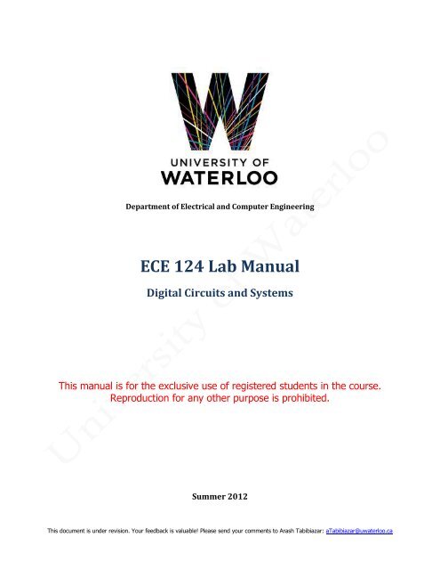
Department of <strong>Electrical</strong> <strong>and</strong> <strong>Computer</strong> <strong>Engineering</strong><br />
ECE 124 <strong>Lab</strong> <strong>Manual</strong><br />
Digital Circuits <strong>and</strong> Systems<br />
This manual is for the exclusive use of registered students in the course.<br />
Reproduction for any other purpose is prohibited.<br />
<strong>Summer</strong> <strong>2012</strong><br />
This document is under revision. Your feedback is valuable! Please send your comments to Arash Tabibiazar: aTabibiazar@uwaterloo.ca
ECE124 <strong>Lab</strong> <strong>Manual</strong> - Digital Circuits <strong>and</strong> Systems<br />
https://ece.uwaterloo.ca/~ece124/<br />
Table of Contents<br />
1 Introduction 3<br />
1.1 Field Programmable Gate Arrays (FPGAs) 4<br />
1.2 Altera Quartus-II FPGA design software 5<br />
1.3 DE2 FPGA board peripherals 5<br />
1.3.1 Light Emitting Diodes (LEDs) 6<br />
1.3.2 7-Segment display 6<br />
1.4 VHDL basics 6<br />
2 <strong>Lab</strong> 1 – Design entry using Altera Quartus-II 7<br />
2.1 Prelab 7<br />
2.2 VHDL design entry using Altera Quartus-II 7<br />
2.2.1 Pin assignment 7<br />
2.2.2 Adding VHDL codes 8<br />
2.2.2.1 Underst<strong>and</strong>ing VHDL structure 8<br />
2.2.2.2 Underst<strong>and</strong>ing the VHDL code 8<br />
2.2.3 Compiling the design for the FPGA 9<br />
2.2.4 Simulation 9<br />
2.2.5 Timing analysis 11<br />
2.2.6 Programming the FPGA 12<br />
2.2.7 Test the design on DE2 board 12<br />
2.3 Design your own circuit – Car-Controller 12<br />
2.4 Postlab 13<br />
3 <strong>Lab</strong> 2 – Combinational circuits; Arithmetic Logic Unit - VHDL Design 14<br />
3.1 Prelab 14<br />
3.2 <strong>Lab</strong> requirement – ALU VHDL design 14<br />
3.3 Postlab 16<br />
4 <strong>Lab</strong> 3 – Combinational circuits; Elevator Controller – Schematic design 17<br />
4.1 Prelab 17<br />
4.2 Schematic design entry using Altera Quartus-II 17<br />
4.3 <strong>Lab</strong> requirement – EC schematic design 18<br />
4.4 Postlab 19<br />
5 <strong>Lab</strong> 4 – Sequential circuits; Traffic Light Controller – VHDL design 20<br />
5.1 Prelab 21<br />
5.2 <strong>Lab</strong> requirement – Part A: A Simple Sequencer 21<br />
5.3 Postlab – Part A only 23<br />
5.4 <strong>Lab</strong> requirement – Part B: TLC VHDL design 23<br />
5.5 Postlab 25<br />
6 Appendix I – DE2 pin assignment file 26<br />
2
1 Introduction<br />
ECE124 <strong>Lab</strong> <strong>Manual</strong> - Digital Circuits <strong>and</strong> Systems<br />
https://ece.uwaterloo.ca/~ece124/<br />
The <strong>Lab</strong> Experiments are done in groups of two. Find a lab partner as soon as possible. Each laboratory<br />
experiment has several parts:<br />
1. A prelab that must be done before coming to the lab. This will include material to read, <strong>and</strong> a<br />
circuit to design.<br />
2. A three-hour laboratory session during which help is available, progress is demonstrated, <strong>and</strong><br />
debugging is done.<br />
3. A final report, due is 4:30pm, one day after your demo, regarding the guidelines in the lab manual.<br />
To minimize the VHDL <strong>and</strong> simulation print-outs use 2-up, double sided, <strong>and</strong> l<strong>and</strong>scape<br />
orientation. Late lab reports will lose mark 10 % per day.<br />
4. Absolutely no food or drink in the laboratories. Do not leave the doors or windows open. The<br />
room will be closed after hours if the rules cannot be followed.<br />
5. You must make a reasonable attempt at the labs in order to pass the course. Failure to do so will<br />
result in a grade of INComplete.<br />
Each workstation in the ECE 124 lab is equipped with:<br />
1. Altera DE2 Board housing a Cyclone II Field Programmable Gate Array (FPGA) chip <strong>and</strong> a<br />
multitude of peripheral components<br />
2. Altera Quartus-II FPGA Design Software<br />
In this section you are going to be briefly introduced the on-board components.<br />
Figure 1 The DE2 board<br />
3
ECE124 <strong>Lab</strong> <strong>Manual</strong> - Digital Circuits <strong>and</strong> Systems<br />
https://ece.uwaterloo.ca/~ece124/<br />
Figure 2 FPGA block diagram of DE2 board<br />
1.1 Field Programmable Gate Arrays (FPGAs)<br />
A FPGA is a Field Programmable Gate Array; basically an array of generic gates to perform any logic<br />
function. Many FPGAs simply use small blocks of memory, called CLBs (Combinational Logic Blocks), to<br />
look up the answer to equations of 4 or 5 variables. In the past, AND <strong>and</strong> OR gates would be<br />
interconnected to solve equations; but this has been replaced with CLB's as they are more flexible <strong>and</strong> can<br />
be used as memory blocks.<br />
As not all equations have as little as 4 variables; typical designs will be spread over several CLBs;<br />
requiring signals to be routed between the CLBs. Just how much circuitry there is, <strong>and</strong> how fast it will run,<br />
in a particular FPGA, depends upon the speed of CLBs, the amount of resources for routing signals<br />
between CLBs, <strong>and</strong> how well a design can be "laid out" or optimized.<br />
4
ECE124 <strong>Lab</strong> <strong>Manual</strong> - Digital Circuits <strong>and</strong> Systems<br />
https://ece.uwaterloo.ca/~ece124/<br />
Newer FPGAs are tailored for specific circuits. The Cyclone II FPGA, which is in our labs, has hardware<br />
multipliers <strong>and</strong> adders, which run at 250MHz, allowing ultra-fast digital signal processing circuits to be<br />
built.<br />
Configurable interconnects are provided between the chip resources (CLBs, hardware multipliers <strong>and</strong><br />
memory blocks for the Cyclone II FPGA). The logic, circuitry, <strong>and</strong> interconnects in the architecture are<br />
configured by uploading a programming file to the FPGA chip. This property makes the FPGA chip very<br />
flexible since it is able to realize different digital circuits by uploading a different programming file. FPGAs<br />
are different that microprocessors or microcontrollers because the designer is able to change the<br />
hardware realized by the chip by programming it. Since hardware is always faster than software FPGAs<br />
allow hardware to be built with nearly the speed of software development.<br />
1.2 Altera Quartus-II FPGA design software<br />
Quartus is a full FPGA design software suite. It aids the designer through the different stages of describing<br />
the hardware design <strong>and</strong> targeting it for a certain Altera FPGA chip. The design process proceeds through<br />
the following stages:<br />
� Design Entry: allows the designer to enter a hardware design specification using:<br />
o Hardware Description Language: such as VHDL or Verilog (we use VHDL)<br />
o Schematic Entry: by connecting blocks of ranging complexity. It can be used to<br />
interconnect simple components such as simple logic gates, or to interconnect previously<br />
created hardware modules<br />
� Design Compilation: Once the design has been specified <strong>and</strong> entered into the tool, the designer<br />
must perform compilation which will take the design through various steps:<br />
o Analysis <strong>and</strong> Synthesis: A HDL or schematic file is analyzed <strong>and</strong> the hardware is broken<br />
down <strong>and</strong> mapped to the device resources (CLBs, flip flops, memory elements, .. etc) so<br />
that design logic is implemented via the available resources on the target chip<br />
o Place <strong>and</strong> Route: actual placement of design on certain device resources <strong>and</strong> routing it<br />
through the programmable interconnection take place in this step<br />
o Assembly: a programming file is produced so that it can be uploaded to the FPGA chip<br />
� Circuit Simulation: In order for a designer to verify the functionality of their design simulation is<br />
required. The simulation step ensures that the circuit operates in the expected manner. A<br />
simulator is fed with the design description files <strong>and</strong> waveforms describing the input values<br />
against time to the circuit under test. The simulator then produces the logic values that will<br />
appear on the circuit outputs as waveforms also against time.<br />
� Timing Analysis: It gives an accurate indication of how fast the circuit runs, <strong>and</strong> if speed <strong>and</strong><br />
timing constraints can be met. Electronic circuits always have speed requirements to be met <strong>and</strong><br />
being able to ballpark how fast a design works without having to build <strong>and</strong> measure it greatly<br />
speeds up design time.<br />
� Programming the FPGA: In this step the programming file is uploaded to the FPGA chip to realize<br />
the design. The circuit can be physically tested afterwards by applying inputs <strong>and</strong> observing<br />
outputs<br />
1.3 DE2 FPGA board peripherals<br />
The DE2 board is equipped with peripherals that can be used to create various applications such as<br />
SDRAM, SRAM <strong>and</strong> flash memory chips, SD card socket, audio CODEC, VGA digital to output convertor <strong>and</strong><br />
5
ECE124 <strong>Lab</strong> <strong>Manual</strong> - Digital Circuits <strong>and</strong> Systems<br />
https://ece.uwaterloo.ca/~ece124/<br />
many others. For the purposes of the labs we are only using switches <strong>and</strong> push buttons for supplying<br />
inputs <strong>and</strong> the following peripherals for displaying outputs:<br />
1.3.1 Light Emitting Diodes (LEDs)<br />
LEDs are electronic components which can emit light with much greater efficiency than inc<strong>and</strong>escent<br />
lamps. The Altera DE2 board has many outputs but you will only use the LEDs.<br />
1.3.2 7-Segment display<br />
A 7-segment decoder takes an input, typically a 4 bit binary number, <strong>and</strong> correctly drives a 7-segment<br />
LED display so that a person can see a number or letter as opposed to trying to interpret the original 4 bit<br />
binary number.<br />
The 7-segment display is so called because it is 7 bar shaped LEDs arranged in such a way that the<br />
numbers 0 to 9, <strong>and</strong> letters A to F, can be displayed. Seven segments is the minimum number which can<br />
uniquely display numbers <strong>and</strong> that is why they are used for many calculator or electronic displays.<br />
1.4 VHDL basics<br />
VHDL is a language used by a hardware designer to describe the behavior of hardware. A synthesis tool<br />
then converts this into a circuit to be built. VHDL is helpful for the design of digital circuits, <strong>and</strong> is one of<br />
two main languages in use; the other being Verilog. An array of other languages is becoming popular such<br />
as SystemC <strong>and</strong> recently SystemVerilog. Basic circuit constructs such as AND, OR, NOT (gates) <strong>and</strong> lookup<br />
tables (SELECT statement), counters <strong>and</strong> flip-flops are straight forward. The VHDL language is very<br />
complex <strong>and</strong> was originally designed for the simulation of most anything. We encourage you to use the<br />
provided examples <strong>and</strong> stick with what you know will work. The most basic rule of VHDL is that if you<br />
can't underst<strong>and</strong> how the CAD tool will create the circuit within the FPGA; then it's unlikely that the<br />
design will do what you expect. Because of this, it is vital that you have an underst<strong>and</strong>ing of basic logic<br />
circuitry <strong>and</strong> design.<br />
6
ECE124 <strong>Lab</strong> <strong>Manual</strong> - Digital Circuits <strong>and</strong> Systems<br />
https://ece.uwaterloo.ca/~ece124/<br />
2 <strong>Lab</strong> 1 – Design entry using Altera Quartus-II<br />
The goal of this lab session is to gain experience with the Altera Quartus FPGA design software with both<br />
circuit entry <strong>and</strong> simulation <strong>and</strong> then modifying the provided circuits. The student will be programming<br />
the FPGA to verify that the circuit works in hardware. No prior experience with digital design, Altera<br />
Quartus or FPGAs is necessary; although experience with basic digital logic will enable one to underst<strong>and</strong><br />
the circuit.<br />
2.1 Prelab<br />
No prelab work is necessary for the first part, the introduction, of this lab experiment. A simple<br />
multiplexer circuit has been provided. After the self-guided introduction the student will modify this<br />
circuit to perform a different task. The lab starts with a brief introduction to the laboratory room, the<br />
equipment <strong>and</strong> the lab experiments. <strong>Lab</strong> 1 is composed of four parts in which you will:<br />
1. Design entry of a VHDL code for a small digital circuit<br />
2. Simulate the circuits to check that they operate correctly<br />
3. Program the FPGA <strong>and</strong> check that the hardware implementation functions correctly<br />
4. Modify the provided circuit to provide new functionality, simulate & test it <strong>and</strong> submit a report<br />
2.2 VHDL design entry using Altera Quartus-II<br />
To start the software click Start then select the program group Altera. Then click on the Altera Quartus II<br />
icon. To create a project select File -> New Project Wizard <strong>and</strong> then enter as much information as you<br />
wish. Create a new project called <strong>Lab</strong>1. In project wizard page 1 you must set a working directory for<br />
your project. You should use “N:\ECE124\<strong>Lab</strong>1" or something similar; creating a unique, logical,<br />
directory name which describes your project. Next you must select the name of your project that must be<br />
the same name as your top level design entity (<strong>Lab</strong>1). Then click on Next <strong>and</strong> say yes for the creation of<br />
the directory. Page 2 then allows you to add VHDL files to your project. Skip this now by clicking on Next.<br />
In page 3 you must select the Altera FPGA family Cyclone II, <strong>and</strong> EP2C35F672C6 from available devices.<br />
In particular the DE2 board uses a FBGA package with 672 pins, <strong>and</strong> speed grade 6. Once you've<br />
selected the correct part you should select Finish in order to skip the next page.<br />
2.2.1 Pin assignment<br />
Pin assignment is the process which maps the input <strong>and</strong> output signals of your design to physical pins of<br />
the FPGA chip available on the hardware board. As mentioned earlier the chip has a vast amount of<br />
resources <strong>and</strong> the design can be built anywhere on the chip in the place <strong>and</strong> route step. The inputs <strong>and</strong><br />
outputs can be exported to any pins on the chip. Pin assignments act as constraints to specify where<br />
exactly your pins are going to be exported <strong>and</strong> are necessary as the peripherals are already pre-wired. To<br />
use different DE2 board peripherals such as LEDs, buttons <strong>and</strong> switches we must go through pin<br />
assignment. Since each peripheral is connected physically to a certain pin in the FPGA on the board, we<br />
should make sure the tool exports our inputs <strong>and</strong> outputs to the peripherals we target for use. Pin names<br />
are complex to use so the pins assignment file gives a logical name to each pin to be used throughout the<br />
design <strong>and</strong> maps it to a certain physical pin name. You can open the supplied file to see how this mapping<br />
is done.<br />
7
ECE124 <strong>Lab</strong> <strong>Manual</strong> - Digital Circuits <strong>and</strong> Systems<br />
https://ece.uwaterloo.ca/~ece124/<br />
Download the supplied pin assignment file (DE2_pins.csv) from course web site <strong>and</strong> save it in your<br />
project directory. Click on Assignments->Import Assignments, then click on the [...] to select the saved<br />
pin assignment file (DE2_pins.csv), which you've saved to your working directory <strong>and</strong> click OK.<br />
For the Altera DE2 FPGA board, unused pins should all be left as inputs tri-stated. Unfortunately the<br />
default is to ground unused pins (this reduces noise <strong>and</strong> is what one should do for a product to be<br />
shipped). To change this setting click on Assignments->Settings then select the Device category <strong>and</strong><br />
click on Device & Pin Options then select the Unused Pins tab <strong>and</strong> change the value to Input tri-stated.<br />
Click OK twice to close the windows.<br />
2.2.2 Adding VHDL codes<br />
You may use a VHDL or Schematic (Block Diagram) design in your project. For this part of lab, download<br />
the “lab1.vhd” file from web site <strong>and</strong> add this file to your project directory. To add it to the project, click<br />
on Project->Add/Remove Files in Project, find <strong>and</strong> select the VHDL file on your local directory <strong>and</strong> click<br />
Add <strong>and</strong> the OK.<br />
2.2.2.1 Underst<strong>and</strong>ing VHDL structure<br />
VHDL is case insensitive. For this reason many coders use all lower case. VHDL language uses two main<br />
structures to describe a design unit (hardware block):<br />
1. Entity: it declares the design unit name <strong>and</strong> the ports (which are inputs <strong>and</strong> outputs of the entity<br />
or design unit) associated with it. Each port name, type (input or output) <strong>and</strong> width (number of<br />
bits) is declared in the entity.<br />
2. Architecture: the architecture specifies the actual functionality of the entity. Notice that the<br />
entity has no information about how the hardware block uses the inputs to produce the outputs -<br />
that is the role of the architecture associated with the entity.<br />
There are two ways to describe the functionality of a certain block:<br />
1. Behavioral: where the relation between input <strong>and</strong> output is declared using logical equations.<br />
2. Structural: where you can use previously created entities in your design unit as components. For<br />
example if you built an adder unit you can use it, as a component, in designing a microprocessor.<br />
2.2.2.2 Underst<strong>and</strong>ing the VHDL code<br />
Underst<strong>and</strong>ing the given VHDL code will help you in the upcoming labs. The given code consists of one<br />
design unit (single entity <strong>and</strong> architecture). “<strong>Lab</strong>1” is the top level entity for the design. It has 2 input<br />
ports (key <strong>and</strong> sw) <strong>and</strong> 2 output ports (ledr <strong>and</strong> ledg). Notice that the names of the ports are case<br />
insensitive <strong>and</strong> identical to those ones in the pins assignment files <strong>and</strong> are similar to the names on the<br />
DE2 board. We are using those logical names in order to map our inputs to the keys, switches, red <strong>and</strong><br />
green LEDs respectively. Analyze the code <strong>and</strong> try to familiarize yourself with VHDL, it is fully<br />
commented. If you still cannot figure out a certain line ask for help.<br />
8
2.2.3 Compiling the design for the FPGA<br />
ECE124 <strong>Lab</strong> <strong>Manual</strong> - Digital Circuits <strong>and</strong> Systems<br />
https://ece.uwaterloo.ca/~ece124/<br />
To compile the design <strong>and</strong> make a programming file for the FPGA click on Processing->Start<br />
Compilation or use “Ctrl+L” or the arrow button on the toolbar. You will see around 100 messages;<br />
mostly due to pins which have been defined but are not being used. Near the bottom of the Quartus II<br />
window you will see several tabs. You can click on Warning or Critical Warning or Error or Info<br />
messages to see the details. You should always check the Error <strong>and</strong> Critical Warning messages <strong>and</strong><br />
resolve them. Prudent users should also check the Warning messages if the design isn't working as<br />
expected. If there are any error(s), compilation will be stopped <strong>and</strong> one can read the error message(s),<br />
divine the problem <strong>and</strong> fix it. Expect to see many warnings because of the pin assignment file as it defines<br />
almost every pin on the FPGA <strong>and</strong> you will be warned, at least once, for each one that is not connected.<br />
The following steps are done by the software to convert the schematic circuit <strong>and</strong>/or HDL (e.g. VHDL,<br />
Verilog) circuit into a file which is used to program the FPGA:<br />
� Analysis & Synthesis: This stage converts the design into parts which are available within the<br />
selected FPGA. Parts which are available are typically flip flops, memory blocks, look-up tables<br />
<strong>and</strong> adders; <strong>and</strong> sometimes multipliers <strong>and</strong> other complex support parts.<br />
� Fitter: This places the parts within an FPGA, connects them together <strong>and</strong> to the input <strong>and</strong> output<br />
pins, <strong>and</strong> optimizes the layout for the user goals (typically speed). A design may require hundreds,<br />
or thous<strong>and</strong>s of CLBs (Combinational Logic Elements), LEs (Logic Elements) or LUTs (Look-Up<br />
Tables).<br />
� Assembler: Converts the fitted design into a file which can be used to program the FPGA.<br />
2.2.4 Simulation<br />
Altera Quartus-II comes with a simple simulator which is limited by its graphical nature. The input<br />
stimulus is applied as waveforms, <strong>and</strong> then the simulation is run <strong>and</strong> the output analyzed. The simulation<br />
is not interactive, <strong>and</strong> so can be quite slow for debugging. It also does not allow one to view anything but<br />
input <strong>and</strong> output pins <strong>and</strong> internal registers.<br />
To simulate your circuit, a vector waveform File must be created. This specifies the inputs to the circuit.<br />
To do this click on File->New then select the Verification/Debugging Files tab <strong>and</strong> select Vector<br />
Waveform File. That will open a file typically called Waveform1.wmf. In the left window of that file, right<br />
click <strong>and</strong> select Insert Node or Bus <strong>and</strong> then click on the Node Finder button. In the filter tab scroll up<br />
<strong>and</strong> select Pins: Input <strong>and</strong> then click the List button to show all input pins. Click on the ">" arrow to add<br />
these input pins sw(0), sw(1), sw(3), <strong>and</strong> key(0) to the Selected Nodes column. You could repeat this for<br />
Pins: Output (ledg[0], ledg[1], ledr[0]) but this is not necessary as the simulator adds all outputs by<br />
default, then click OK. For simulation you need to set a series of ‘0’s or ‘1’s to inputs (input test pattern).<br />
To assign periodic values, right click on a signal <strong>and</strong> select Value->Clock <strong>and</strong> then set the following<br />
period for each signal (Table 1). It will switch each signal between ‘0’ <strong>and</strong> ‘1’ at a certain interval. By<br />
choosing intervals that increase by a factor in power of two ( ), all possible combinations<br />
of inputs will be generated (Figure 3).<br />
Table 1 Input signals clock assignments<br />
Inputs sw[0] sw[1] sw[3] key[0]<br />
Period 50ns 100ns 200ns 400ns<br />
9
ECE124 <strong>Lab</strong> <strong>Manual</strong> - Digital Circuits <strong>and</strong> Systems<br />
https://ece.uwaterloo.ca/~ece124/<br />
Don’t forget to hit “Ctrl+W” or right click in the waveform window <strong>and</strong> select Zoom->Fit in Window. By<br />
these assignments, all possible combinations to the inputs will be generated (an exhaustive test), which is<br />
only suitable for automated testing or where there are a few combinations to visually check. The “OR” <strong>and</strong><br />
“AND” logic gates are easy to verify. One can force inputs to values other than a periodic wave. For<br />
instance, the Value->Count Value lets you go through all possible inputs - as does the r<strong>and</strong>om method -<br />
but for a more complex circuit one would test specific combinations of inputs, not all. When you are done<br />
creating your vector waveform inputs, you should save the resulting file into your project directory.<br />
Figure 3 Exhaustive test input generation for function F(X0,X1,X2,X3) = ~X0 & ~X1 & ~X2 & X3<br />
There are two types of simulation:<br />
� Functional: This is a verification of the basic functionality of the circuit with no timing<br />
information (i.e. gate delays) included.<br />
� Timing: Timing simulation uses information about the circuit design, <strong>and</strong> how the circuit is fit<br />
into an FPGA, to estimate accurate time delays for signals. This simulation is slower; but it is also<br />
necessary to determine if a design can meet the speed requirements.<br />
Now, you can run the simulator by clicking on Processing->Simulator Tool. Set the End simulation at<br />
value to 1us (default). Then Select Timing as Simulation mode. For the Simulation Input field select your<br />
simulation file just created. Then click on Start. Wait until it finishes <strong>and</strong> then click the Report button to<br />
see the simulator output. Hit “Ctrl-W”, or right click <strong>and</strong> choose Zoom->Fit in Window to view the entire<br />
simulation.<br />
Remember from “lab1.vhd” code (line 45) that for example: “ledg (0) = sw (0) | sw (1)”.<br />
10
ECE124 <strong>Lab</strong> <strong>Manual</strong> - Digital Circuits <strong>and</strong> Systems<br />
https://ece.uwaterloo.ca/~ece124/<br />
Figure 4 Timing-mode simulation report for <strong>Lab</strong>1.vhd design<br />
For timing simulation, you may notice that there are some very narrow spikes. These are glitches due to<br />
the circuit, or the way that simulation is done <strong>and</strong> can be generally ignored for this course. You'll also<br />
notice that there is an approximately 10ns delay between the inputs changing <strong>and</strong> the outputs changing.<br />
Under View, or via the magnifying glass icons, you will find zoom controls. Zoom out to show the full<br />
simulation.<br />
Sometimes, a functional simulation is also required in each lab. You must Select Functional as Simulation<br />
mode <strong>and</strong> then click on Generate Functional Simulation Netlist tab to generate the necessary files. For<br />
a functional simulation, you will not see any time delay. Here is a sample result of a timing simulation,<br />
verify its functionality matches with the VHDL code.<br />
2.2.5 Timing analysis<br />
Timing analysis can only be run after a design is successfully implemented <strong>and</strong> it gives an accurate<br />
indication of how fast the circuit runs, <strong>and</strong> if speed <strong>and</strong> timing constraints can be met. Electronic circuits<br />
always have speed requirements to be met <strong>and</strong> being able to ballpark how fast a design works without<br />
having to build <strong>and</strong> measure it greatly speeds up design time. To run the analyzer, click on Processing-<br />
>Classic Timing Analyzer Tool <strong>and</strong> click the Start button. Click on the tpd tab <strong>and</strong> note that the slowest<br />
signal is at the top of the list. This is the time delay from "P2P" (Pin to Pin). You likely have a value around<br />
11ns. Other tabs provide you time delays for more complex circuits with flip-flops.<br />
By default, all paths in the circuit get analyzed <strong>and</strong> listed. There are two categories to consider:<br />
� tpd: This is the time required for a signal to go from an input pin to an output pin through<br />
combinational logic<br />
11
ECE124 <strong>Lab</strong> <strong>Manual</strong> - Digital Circuits <strong>and</strong> Systems<br />
https://ece.uwaterloo.ca/~ece124/<br />
� tco: For registers <strong>and</strong> flip-flops, this is the time required for an output to become valid after the a<br />
clock signal transition. Also pay attention to the tSU table. That table lists the length of times for<br />
which each data must be present (setup) before the clock transition. So the worst case is the<br />
slowest sum for tCO plus any associate setup times. Note that we've neglected the hold time of the<br />
data for clocked data <strong>and</strong> this can be important in real-world designs.<br />
To quickly get timing information, click on the Report button <strong>and</strong> note the first row information ("Worstcase<br />
tpd"). From this analysis one can see that the circuit would work at a maximum speed of >90MHz;<br />
which isn't very fast compared to the 3+GHz speed of modern computers. However, much more complex<br />
circuits would also work at the same speed, <strong>and</strong> this FPGA has other resources such as adders <strong>and</strong><br />
multipliers which work at 250MHz allowing for real-time HDTV image manipulation.<br />
2.2.6 Programming the FPGA<br />
Make sure that the power to the FPGA board is on (the red button in the upper right corner). The<br />
programmer tool can be found under Tools->Programmer. You will need to make sure that the correct<br />
programmer is selected. Click on Hardware Setup <strong>and</strong> select USB-Blaster, if necessary. Ensure that the<br />
“Currently selected hardware” says USB-Blaster [USB-?]. Next, ensure that for your project the “<strong>Lab</strong>1.sof”<br />
file in the list has a check mark in the box under “Program/Configure”, <strong>and</strong> then just click on the Start<br />
button in order to program the FPGA.<br />
2.2.7 Test the design on DE2 board<br />
Now the design can be tested on FPGA board. Verify the functionality regarding to the “lab1.vhd” file:<br />
� Turn on/off SW0 <strong>and</strong> SW1 inputs, to verify the functions behind outputs LEDG0 <strong>and</strong> LEDG1<br />
(check with VHDL code in lab1.vhd)<br />
� Turn on/off SW1, SW3 <strong>and</strong> KEY0 inputs to verify the function behind output LEDR0 (check with<br />
VHDL code in lab1.vhd)<br />
2.3 Design your own circuit – Car-Controller<br />
For your demo, modify the “lab1.vhd” code to make its function as an automotive controller. The inputs<br />
<strong>and</strong> outputs are defined in below table.<br />
Table 2 Car-Control circuit IO definition<br />
Signal Type Signal Name Assigned Port Description<br />
Gas KEY[0]<br />
Inputs<br />
Clutch<br />
Brake<br />
KEY[1]<br />
KEY[2]<br />
Override SW[1] Master switch to shut down the car<br />
Outputs<br />
GasControl<br />
BrakeControl<br />
LEDG[0]<br />
LEDR[0]<br />
When ON (logic ‘1’), acceleration is given to the motor<br />
When ON (logic ‘1’), the brakes are engaged<br />
12
ECE124 <strong>Lab</strong> <strong>Manual</strong> - Digital Circuits <strong>and</strong> Systems<br />
https://ece.uwaterloo.ca/~ece124/<br />
Consider the following guidelines in your design. A typical block diagram for your design is also shown.<br />
� The pushbuttons (KEY[3:0]) on the DE2 board are inverted. They are ‘1’ when NOT pressed <strong>and</strong><br />
become ‘0’ when pressed.<br />
� Note that some keys (KEY[3:0]) or switches (SW[17:0]) do not work properly sometimes (have<br />
physical damage). Replace them with other ones.<br />
� Make sure that the inputs <strong>and</strong> outputs you need are in the VHDL code ENTITY declaration.<br />
Remove extra ports <strong>and</strong> signals from the design.<br />
� Add a brake safety so that the “Brake” being ON, turns off the “GasControl”.<br />
� Add a clutch safety so that the “Clutch” being ON, turns off the “GasControl”.<br />
� Add an engine safety so that the “Override” being ON, turns off the “GasControl” <strong>and</strong> turns on the<br />
“BrakeControl”.<br />
2.4 Postlab<br />
Figure 5 Car-Control circuit block diagram<br />
Download, print <strong>and</strong> fill out the “<strong>Lab</strong>1SubmissionForm.pdf” from <strong>and</strong> demonstrate your Car-Control<br />
design on scheduled date. Then h<strong>and</strong> in the report, one day after demo session. The submitted report for<br />
Car-Control design must include:<br />
1. Completed “<strong>Lab</strong>1SubmissionForm” as the report front page. Don’t forget to fill out the “total logic<br />
elements” in the form.<br />
2. Implementation procedure, design decisions, encountered problems or bugs with solution to<br />
them <strong>and</strong> debugging techniques (2 pages max). Don’t forget to include the RTL view of your circuit<br />
(Tools->Netlist Viewers->RTL Viewer).<br />
3. Fully commented VHDL code printout (2-up, l<strong>and</strong>scape <strong>and</strong> double sided). Use meaningful name<br />
for your signals.<br />
4. Timing simulation waveform for the circuit showing that the circuit works in all cases (exhaustive<br />
test).<br />
13
ECE124 <strong>Lab</strong> <strong>Manual</strong> - Digital Circuits <strong>and</strong> Systems<br />
https://ece.uwaterloo.ca/~ece124/<br />
3 <strong>Lab</strong> 2 – Combinational circuits; Arithmetic Logic Unit - VHDL Design<br />
The goal is to build a simple VHDL circuit to choose between various calculations <strong>and</strong> logical operations.<br />
This is basically a calculator which can perform multiple operations with no memory, i.e. the circuit is<br />
completely combinational.<br />
3.1 Prelab<br />
First download the “lab2.vhd” code from web site <strong>and</strong> open it a context sensitive editor or Quartus II. At<br />
the top of the file, a new entity for a seven-segment is defined. Try to underst<strong>and</strong> its IO mapping (ENTITY)<br />
<strong>and</strong> function (ARCHITECTURE). In this lab, we will instantiate this entity multiple times to display binary<br />
values in hexadecimal format.<br />
3.2 <strong>Lab</strong> requirement – ALU VHDL design<br />
Create a new project for <strong>Lab</strong>2 <strong>and</strong> add the “lab2.vhd” file to the project. After compiling, program your<br />
FPGA to watch its functionality. For every VHDL design entry, you need to follow all instructions in<br />
section 2.2. Test the circuit with different combinations of input signal values <strong>and</strong> check its output with<br />
the VHDL code.<br />
Now, for your demo, modify the code in “lab2.vhd” to make its function as an ALU. The inputs <strong>and</strong> outputs<br />
are defined in Table 3. You may use other meaningful signal names in your design. Again, you need to<br />
follow all instructions in section 2.2.<br />
Table 3 ALU design IO definition<br />
Signal Type Signal Name Assigned Port Comment<br />
Oper<strong>and</strong> 1 SW[7..0] 8-bit input to be displayed on HEX5 <strong>and</strong> HEX4<br />
Inputs Oper<strong>and</strong> 2 SW[15..8] 8-bit input to be displayed on HEX7 <strong>and</strong> HEX6<br />
Operator SW[17..16] 2-bit input to be displayed on LEDR[17..16]<br />
Outputs OperationResult HEX2,HEX1,HEX0 9-bit output result to be displayed on LEDR[8..0] too<br />
Your design is supposed to implement a simple calculator with four pre-defined operations.<br />
Table 4 ALU operations<br />
SW[17..16] Operator Description<br />
00 AND Logical AND of 8-bit inputs<br />
01 OR Logical OR of 8-bit inputs<br />
10 XOR Logical XOR of 8-bit inputs<br />
11 ADD Binary ADD of 8-bit inputs<br />
Consider the following guidelines in your design. A typical block diagram for your design is also shown.<br />
� SW[7..0] <strong>and</strong> SW[15..8] represent the inputs from most significant bit (MSB) down to least<br />
significant bits (LSB) for the first <strong>and</strong> second oper<strong>and</strong>s. Here, SW[7] <strong>and</strong> SW[15] are most<br />
significant bits.<br />
14
ECE124 <strong>Lab</strong> <strong>Manual</strong> - Digital Circuits <strong>and</strong> Systems<br />
https://ece.uwaterloo.ca/~ece124/<br />
� The result is displayed on HEX2, HEX1 <strong>and</strong> HEX0. HEX2 shows the most significant hex digit of the<br />
result, while HEX0 shows the least significant hex digit of the result. This makes your result<br />
readable on the board. Notice that we are using 3 hex digits to display the result, though we have<br />
8-input oper<strong>and</strong>s. That’s because addition of two 8-bit numbers can cause carry (9 th bit) to occur.<br />
This is the only case in which HEX2 will display 1 instead of being blank. To blank HEX2 use the<br />
blanking input to blank or turn it off.<br />
� Signals are intermediate values that must be declared using “signal” statement in the VHDL<br />
architecture before the “begin” statement.<br />
� Simulation for this lab has some extra complications. Do not add the vector for the inputs (e.g. KEY<br />
or SW) but add individual wires (e.g. KEY[0) <strong>and</strong> when they are added, in the Vector Waveform<br />
File one can group them together. One bundle of 8 wires can be labeled as "A". To group wire<br />
together, select them <strong>and</strong> then press right click <strong>and</strong> choose "Grouping->Group".<br />
� To assign values to input oper<strong>and</strong>s <strong>and</strong> operators, first group them with meaningful signal names<br />
<strong>and</strong> then use “Value->Arbitrary Value", “Value->R<strong>and</strong>om Values” or “Value->Count Value”.<br />
� Instead of looking at the raw 7-segment outputs in the simulator report (they are not meaningful),<br />
it makes more sense to look at the LEDR[8..0] value (group them together) to have faster <strong>and</strong><br />
more intuitive testing. Remember to display the operation result on LEDR[8..0].<br />
� A WHEN statement can be used instead of an IF statement to implement a multiplexer as we have<br />
in sample VHDL file “lab2.vhd”. This multiplexer should be taken into consideration. As mentioned<br />
earlier, HEX2 only displays the carry out value in ADD operation. This can be achieved by<br />
concatenation of A <strong>and</strong> B to a string of 4 zeros <strong>and</strong> then performing addition. This will preserve<br />
carry <strong>and</strong> should produce a 12 bit result. This result can be used to drive the 3 seven segment<br />
decoders. This is the heart of the project <strong>and</strong> will take 5 lines of VHDL code.<br />
� Note that if the result is declared as a 12-bit signal, all operations must produce 12 bit results. So<br />
concatenation is not only required only for addition but also for all other operations too.<br />
� The most difficult part will be the add operation while the result has 9 bits <strong>and</strong> for binary addition<br />
in VHDL signals must be declared in unsigned type. We need to recast the signals to unsigned<br />
type (which are originally in logical type std_logic_vector) <strong>and</strong> then recast again to<br />
std_logic_vector type. You may use statement like this to recast signals:<br />
R
3.3 Postlab<br />
ECE124 <strong>Lab</strong> <strong>Manual</strong> - Digital Circuits <strong>and</strong> Systems<br />
https://ece.uwaterloo.ca/~ece124/<br />
Download, print <strong>and</strong> fill out the “<strong>Lab</strong>2SubmissionForm.pdf” from <strong>and</strong> demonstrate your design on<br />
scheduled date. Then h<strong>and</strong> in the report, one day after demo session. The submitted report must include:<br />
1. Completed “<strong>Lab</strong>2 Submission Form” as the report front page. Don’t forget to fill out the “total logic<br />
elements” <strong>and</strong> the Worst Case Speed (ns) tpd in the form.<br />
2. Implementation procedure, design decisions, encountered problems or bugs with solution to<br />
them, debugging techniques <strong>and</strong> RTL view of your circuit (2 pages max).<br />
3. Fully commented VHDL code printout (2-up, l<strong>and</strong>scape <strong>and</strong> double sided).<br />
4. Functional simulation waveform with coverage for critical cases. Mark your simulation<br />
waveforms explaining several different scenarios for each operation. You must prove that what<br />
you have designed is working. For instance, testing with the inputs set to 0 does not allow one to<br />
distinguish one operation from another or if any operation in particular is fully working. Often one<br />
tests critical cases - the limits where things may break (i.e. overflow). Do not print waveforms of<br />
all possible cases - give samples for critical cases of each operation <strong>and</strong> explain how you checked<br />
for proper operation. The goal is to have a simulation to prove that the circuit works; without<br />
doing a full exhaustive test of all possible inputs. It should prove that all operations work correctly<br />
for enough numbers to give confidence that the circuit is fully functional.<br />
Figure 7 Sample functional simulation output<br />
16
ECE124 <strong>Lab</strong> <strong>Manual</strong> - Digital Circuits <strong>and</strong> Systems<br />
https://ece.uwaterloo.ca/~ece124/<br />
4 <strong>Lab</strong> 3 – Combinational circuits; Elevator Controller – Schematic design<br />
The goal of this lab session is to design two simple circuits using truth tables <strong>and</strong> K-Maps. Translating a<br />
written circuit description into a Truth Table is the basis of this circuit design. Optimizing the design with<br />
K-maps allows one to make the design smaller <strong>and</strong> faster. You are to design <strong>and</strong> implement a circuit to<br />
control an elevator. The circuit has four inputs to define current <strong>and</strong> requested floors <strong>and</strong> two outputs to<br />
enable the motor <strong>and</strong> show the up/down direction.<br />
4.1 Prelab<br />
To prepare for this lab the student should reduce the design descriptions to truth tables. The truth tables<br />
should be then used to build K-Maps. Extract logical expressions from the K-Maps <strong>and</strong> realize the two<br />
circuits required as gates.<br />
4.2 Schematic design entry using Altera Quartus-II<br />
In this lab, we first create a simple project using the schematic editor <strong>and</strong> then modify it to implement<br />
Elevator Controller. To start, create a project <strong>and</strong> name it <strong>Lab</strong>3, repeat the same steps to import the pins<br />
assignment file <strong>and</strong> to set unused pins to input tri-state in section 2.2.1. Proceed by adding the schematic<br />
using the schematic editor. Click on File->New <strong>and</strong> select Design Files->Block Diagram/Schematic<br />
File. Primitive parts (AND, OR, other gates) can be entered via the Symbol Tool which looks like an AND<br />
gate. Click on it <strong>and</strong> then exp<strong>and</strong> the Libraries item to reveal primitives. Exp<strong>and</strong> that to reveal logic<br />
primitives such as gates. You will also need to use the pin <strong>and</strong> other primitives such as input, output,<br />
gnd (ground or logic ‘0’) as well as vcc (high or logic ‘1’). The storage primitives include flip-flops. To<br />
draw wires you will need to use the Orthogonal Node Tool from the toolbox on the left. Drawing wires<br />
can be painful as you will discover. Draw wires in pieces to make the task easier. To connect nets or wires<br />
to the outside world you will also need to use the input <strong>and</strong> output pin primitives. To name your pins just<br />
double click on them <strong>and</strong> use the st<strong>and</strong>ard names (e.g. sw[0], ledg[0]) which is defined in your pin out file,<br />
on the schematic above (documented in Appendix A). Do NOT right click on a wire or node, <strong>and</strong> in the<br />
Properties tab assign a name. That sometimes results in a circuit which does nothing. Now, draw the<br />
schematic shown in Figure 8:<br />
Figure 8 <strong>Lab</strong>3.bdf - Schematic design file<br />
17
ECE124 <strong>Lab</strong> <strong>Manual</strong> - Digital Circuits <strong>and</strong> Systems<br />
https://ece.uwaterloo.ca/~ece124/<br />
Compile this design <strong>and</strong> download it to the FPGA for testing. If you have time, simulate it by setting the<br />
proper input values as clock periods for all possible scenarios (as done in previous labs). Remember to<br />
zoom <strong>and</strong> view the whole simulation with “Ctrl+W”.<br />
4.3 <strong>Lab</strong> requirement – EC schematic design<br />
For your demo, modify the “lab3.bdf” file to make it operate as an elevator controller. The inputs <strong>and</strong><br />
outputs are defined in the Table 5.<br />
Table 5 Car-Control circuit IO definition<br />
Signal Type Signal Name Assigned Port Description<br />
Inputs<br />
CurrentFloor<br />
NextFloor<br />
SW[1..0]<br />
SW[3..2]<br />
Outputs<br />
Enable<br />
Direction<br />
LEDG[0]<br />
LEDR[0]<br />
When ON (logic ‘1’), the motor is turned on<br />
Define moving direction (upwards: ‘1’, downwards:’0’)<br />
Design two versions of this circuit one using any types of 2-input logic gates <strong>and</strong> the other only 2-input<br />
NAND gates. Note that K-maps help you minimize a circuit with any type of gates, but it will not directly<br />
help you to minimize a design where you are restricted to use a specific gate type (e.g. NAND, NOR). There<br />
are two ways to design the circuit:<br />
1. Using only 2-input NAND gates exclusively for the first design <strong>and</strong> minimizing wires <strong>and</strong> gates<br />
using any gates available for the second design<br />
2. Starting with designing a circuit with 2-input logic gates of any types <strong>and</strong> then replacing the gates<br />
with 2-input NAND equivalents<br />
Considering one of above approaches, start the schematic editor to build your two designs using switches<br />
for the four inputs <strong>and</strong> LEDs for the outputs. Simulate your designs <strong>and</strong> upload it to the FPGA for physical<br />
testing.<br />
Consider the following guidelines in your design.<br />
Figure 9 3-floor elevator<br />
18
ECE124 <strong>Lab</strong> <strong>Manual</strong> - Digital Circuits <strong>and</strong> Systems<br />
https://ece.uwaterloo.ca/~ece124/<br />
� You can find a schematic inverter in the Quartus software called NOT under primitives -> logic<br />
� K-Maps should be used to minimize the elevator circuit size. Note that there is no easy way to do<br />
this, for the NAND only design, without lots of experience. Note that there are many things that<br />
can be optimized for. One may choose to design for the minimum number of wires OR gates - it's<br />
hard to minimize both at the same time. We suggest trying this several times <strong>and</strong> include all in<br />
your <strong>Lab</strong> Report.<br />
4.4 Postlab<br />
Download, print <strong>and</strong> fill out the “<strong>Lab</strong>3SubmissionForm.pdf” form <strong>and</strong> demonstrate your design on<br />
scheduled date. Then h<strong>and</strong> in the report, one day after demo session. The submitted report must include:<br />
The submitted report must include:<br />
1. Completed “<strong>Lab</strong>3 Submission Form” as the front page of your report. Don’t forget to fill out the<br />
“number of gates” <strong>and</strong> “number of wires” in the form for demonstrated circuit.<br />
2. Implementation procedure, design decisions, encountered problems or bugs with solution to<br />
them, debugging techniques <strong>and</strong> RTL view of your circuit (2 pages max).<br />
3. Discussion of exp<strong>and</strong>ability of the design if the 4 th floor is added <strong>and</strong> effect of that on reliability<br />
(you don't need to actually implement the 4 th floor extra logic). Consider the number of wires <strong>and</strong><br />
gates as being indicators of reliability.<br />
4. How does the all NAND design compare to the other design? How many gates <strong>and</strong> wires are<br />
required for each? Note: This lab used to be built <strong>and</strong> so you should count ALL gates - inverters<br />
too - as they all had to be wired up. Which would be more reliable?<br />
5. Include the truth table for the elevator controller, K-maps <strong>and</strong> how you deduced logical<br />
expressions for the two circuits.<br />
6. Schematic printout for the two circuits<br />
7. Simulation waveforms for the two circuits showing that they work in all cases (please circle 4<br />
points <strong>and</strong> identify what the inputs represent <strong>and</strong> why the outputs are correct according to the<br />
requirements). Demonstrate that you can interpret the simulation waveforms.<br />
19
ECE124 <strong>Lab</strong> <strong>Manual</strong> - Digital Circuits <strong>and</strong> Systems<br />
https://ece.uwaterloo.ca/~ece124/<br />
5 <strong>Lab</strong> 4 – Sequential circuits; Traffic Light Controller – VHDL design<br />
The goal of this lab is to design a traffic light control system as a sequential circuit with clock. The system<br />
controls two traffic lights on an intersection using a state machine. First you will learn to implement <strong>and</strong><br />
test, two clock dividers using modulus <strong>and</strong> binary counters.<br />
The st<strong>and</strong>ard way to implement a clock divider is to use a binary counter. Binary counters increment<br />
their value by one on every rising/falling edge of its input clock signal. If you consider an n-bit binary<br />
counter, you notice that the first bit of the counter (LSB) toggles in the period of half-speed of the original<br />
clock. If you look at the second bit you would find it toggling at half speed of the first bit which means 1/4<br />
the speed of the original clock. Thus N th bit in the counter output is a clock in frequency of input clock<br />
frequency divide by 2 N+1 where N is the bit position starting from bit 0. The binary counter is not very<br />
accurate if you need a clock signal with precise frequency because the divisor is always in power of two.<br />
So for accurate timing or clock division a modulus counter can be used. A modulus counter increments up<br />
to a certain number (terminal count value) <strong>and</strong> then resets to initial value. It toggles the clock signal at the<br />
terminal which is equal to half the period of your desired output clock. Thus you need to calculate the<br />
period of your clock to determine the terminal value. Figure 10 shows outputs of two 25-bit binary <strong>and</strong><br />
modulus counters generated from a 50MHz input clock.<br />
F0=50MHz<br />
T0=20ns<br />
25-bit Binary Counter<br />
÷33,554,432=2^25<br />
25-bit Modulus Counter<br />
÷25,000,000<br />
20<br />
F~1.49Hz<br />
T~0.67s<br />
F=1Hz<br />
T=1s<br />
Figure 10 Binary <strong>and</strong> Modulus clock dividers by 25-bit counters<br />
16,777,216 × T0<br />
25,000,000 × T0<br />
33,554,432 × T0<br />
50,000,000 × T0<br />
In this lab you need to implement sequential logic in VHDL. Sequential logic has "memory" <strong>and</strong> the output<br />
depends on the inputs <strong>and</strong> what the current state or "memory" is. This requires a PROCESS structure in<br />
your architecture to implement flip-flops <strong>and</strong> other memory elements. It starts with a tag (name)<br />
followed by a colon then the word PROCESS. Between brackets you mention all the signals that affect<br />
your logic (sensitivity list) separated by a comma. These are the signals that will trigger execution of the<br />
process inside the simulator. Thus, any signal utilized in the process logic should be in the sensitivity list.<br />
Missing signals from the sensitivity list cause simulation-synthesis mismatch. The key statement to<br />
implement flip flops or sequential logic, is the IF (rising_edge clock) THEN statement.<br />
In VHDL, state machines are built inside a process block. A case statement can be used to determine the<br />
next state depending on the current state <strong>and</strong> other signals (inputs or time events). On the edge of the<br />
clock the current state is assigned the value of the next state (determined by the case statement). It is<br />
worth mentioning that sometimes your decision can be staying in the same state. To name your states you<br />
may declare a new type in your architecture <strong>and</strong> then declare two signals of this type to keep your current<br />
state <strong>and</strong> next state.
5.1 Prelab<br />
ECE124 <strong>Lab</strong> <strong>Manual</strong> - Digital Circuits <strong>and</strong> Systems<br />
https://ece.uwaterloo.ca/~ece124/<br />
In this lab experiment, it is important to design <strong>and</strong> build your circuit incrementally. Don’t start designing<br />
the whole circuit at once. First download the “lab4.vhd” file from web site <strong>and</strong> open it a context sensitive<br />
editor or Quartus II. Browse the VHDL code carefully <strong>and</strong> try to underst<strong>and</strong> all statements in the file. Look<br />
at the clock divider circuits <strong>and</strong> study how they work, how to change the frequency of the system clock,<br />
<strong>and</strong> how it could be further divided by 10. Try to extract the embedded state machine in this code <strong>and</strong><br />
underst<strong>and</strong> sequential logic design statements in VHDL.<br />
5.2 <strong>Lab</strong> requirement – Part A: A Simple Sequencer<br />
Create a new project for <strong>Lab</strong>4 <strong>and</strong> add the “lab4.vhd” file to the project. For every VHDL design entry, you<br />
need to follow all instructions in section 2.2, i.e., import pin assignment file, set unused pins to tri-state,<br />
compile, program the device, etc. Test the circuit with different combinations of input signal values <strong>and</strong><br />
check its function with the VHDL code. Do not try to simulate the design at this moment.<br />
Now, for your demo, modify the “lab4.vhd” file to make a sequencer to generate the following pattern<br />
(Figure 11) repeatedly on green <strong>and</strong> red LEDs. The pattern starts with a flashing light on a green LED for<br />
two seconds followed by solid pattern for 5 seconds <strong>and</strong> then the same sequence with different durations<br />
on red LED. The inputs <strong>and</strong> outputs are defined in Table 6. You may use other meaningful signal names in<br />
your design. Again, you need to follow all the instructions provided in section 2.2.<br />
0 1 2 3 4 5 6 7 8 9 10 11 12 13 14 15<br />
GFLASH<br />
2s<br />
GSOLID<br />
5s<br />
RFLASH<br />
3s<br />
21<br />
RSOLID<br />
6s<br />
Green LED ON, Red LED OFF Red LED ON, Green LED OFF<br />
Figure 11 Sequencer timing diagram<br />
Table 6 Sequencer circuit IO definition<br />
Signal Type Signal Name Assigned Port Description<br />
Input Input Clock CLOCK_50 50MHz on-board clock<br />
Green LED LEDG[8] Green light pattern<br />
Red LED LEDR[11] Red light pattern<br />
Clock 1Hz Bin LEDG[2] 1Hz output from binary counter<br />
Outputs Clock 1Hz Mod LEDG[1] 1Hz output from modulus counter<br />
Clock 10Hz Mod LEDG[0] 10Hz output from modulus counter<br />
State Number HEX0 4-bit internal state number<br />
State Counter HEX2 4-bit internal state counter<br />
Start your design with modulus 10Hz <strong>and</strong> 1Hz clock dividers. Use this 1Hz clock to drive your state<br />
machine. Keep the binary 1Hz clock output for your demo. Figure 12 shows a typical block diagram for<br />
your design. You must be able to implement the sequencer FSM in four states. Display your internal<br />
signals (state number <strong>and</strong> counter) on Seven-Segment displays to debug your circuit.
User Red LEDs<br />
LEDR[17:0]<br />
User Green LEDs<br />
LEDG[8:0]<br />
ECE124 <strong>Lab</strong> <strong>Manual</strong> - Digital Circuits <strong>and</strong> Systems<br />
https://ece.uwaterloo.ca/~ece124/<br />
LEDR[11]<br />
LEDG[8], LEDG[2:0]<br />
Your<br />
TLC Design<br />
FPGA<br />
22<br />
CLOCK_50<br />
HEX4, HEX0<br />
PIN<br />
PORT<br />
Figure 12 A typical block diagram for a sequencer design<br />
50MHz<br />
7-Segment Display (x8)<br />
Try to build the required components one by one to generate the timing diagram in Figure 11:<br />
1. A modulus clock divider to create a 10Hz clock from the board's 50MHz clock input.<br />
2. A modulus clock divider to create a 1Hz clock from the 10Hz clock.<br />
3. The 1Hz clock will drive a counter to determine the time of transitions between states. The<br />
current state determines which LEDs are ON or OFF. Your states can be defined as:<br />
� GFLASH: the green LED is flashing at 10Hz, while red LED is OFF.<br />
� GSOLID: the green LED is ON, while red LED is OFF.<br />
� RFLASH: the red LED is flashing at 10Hz, while green LED is OFF.<br />
� RSOLID: the red LED is ON, while green LED is OFF.<br />
In order to simulate your design before programming the FPGA device, you should change the terminal<br />
count value for your first modulus counter in clock chain (10Hz) to skip from waiting for 5,000,000 clock<br />
cycles in your simulations to generate one cycle of 10Hz clock from 50MHz. You can set your terminal<br />
count to "0000000000000000000000001" <strong>and</strong> then find a proper clock period for CLOCK_50 to have<br />
exactly 10Hz <strong>and</strong> 1Hz clocks in simulation waveforms (Figure 13).<br />
Another way of simulating your design is completely bypassing the clock divider <strong>and</strong> providing the<br />
50MHz clock to the state machine. Please notice that this strategy is only to simulate your design.<br />
For your simulations<br />
bypass this divider or reduce its length<br />
10Hz Clock Divider<br />
1Hz Clock Divider<br />
F0=50MHz ÷5,000,000<br />
F1=10Hz<br />
÷10<br />
F2=1Hz<br />
Figure 13 Clock generation scheme<br />
DE2
5.3 Postlab – Part A only<br />
ECE124 <strong>Lab</strong> <strong>Manual</strong> - Digital Circuits <strong>and</strong> Systems<br />
https://ece.uwaterloo.ca/~ece124/<br />
Download, print <strong>and</strong> fill out the “<strong>Lab</strong>4SubmissionForm.pdf” form <strong>and</strong> demonstrate your design on<br />
scheduled date. Keep your submission form for the second demo (part B) <strong>and</strong> <strong>Lab</strong>4 report. There is no<br />
lab report required to submit separately for part A. Save your work in a separate project file before<br />
proceeding to TLC design in part B.<br />
5.4 <strong>Lab</strong> requirement – Part B: TLC VHDL design<br />
After building the simple state machine <strong>and</strong> testing that it is functioning according to the given timing<br />
diagram in part A, you are required to extend the designed sequencer in part A to implement a real traffic<br />
light controller in transportation system like Figure 14.<br />
00<br />
A<br />
EW Sensor<br />
NS Sensor<br />
Figure 14 Traffic Light System<br />
23<br />
NS Sensor<br />
The traffic light controller should have two modes of operation (SW[17]).<br />
1. Day Mode: in this mode the traffic light acts normally as a simple sequencer, design in part A to<br />
transit between green, amber <strong>and</strong> red lights in real traffic light systems. As we don’t have yellow<br />
or orange LEDs on our evaluation board, we replace them with a flashing red light in our design.<br />
You may design it in three states as:<br />
� Go: - the green LED is ON. First two seconds is flashing at 10Hz for turning left cars.<br />
� PrepareToStop: the red LED is flashing at 10Hz to warn drivers to be prepared to stop.<br />
� Stop: - the red LED is ON.<br />
As shown in Figure 15, in the day mode, the traffic light controller switches between above states<br />
with the predefined durations (i.e. 6 seconds, 2 seconds <strong>and</strong> 8 seconds respectively) continually.<br />
Note that in the first 2 seconds of “Go” state in this mode, the green LED is flashing.<br />
B<br />
EW Sensor<br />
07
ECE124 <strong>Lab</strong> <strong>Manual</strong> - Digital Circuits <strong>and</strong> Systems<br />
https://ece.uwaterloo.ca/~ece124/<br />
2. Night Mode: in the night mode the traffic light controller has a default side (SW[16]) that traffic<br />
light is always green for it. When the time to switch lights (amber to red) reaches (at the end of<br />
amber light period), if no car is detected on the non-default side, the system starts another greenamber<br />
(only solid green) period for the default side, otherwise it acts like day mode with greenamber-red<br />
periods for both sides. For this mode, we use car detection sensors output for nondefault<br />
side to decide for transition between states. These sensors can be implemented using<br />
ON/OFF switches (SW[15:14]) on the board. When the switch is ON, it indicates the presence of a<br />
car on that side.<br />
Figure 15 Traffic Light Controller Timing Diagram<br />
The inputs <strong>and</strong> outputs for the extended traffic light logic are shown below:<br />
Table 7 TLC circuit IO definition<br />
Signal Type Signal Name Assigned Port Description<br />
Input Clock CLOCK_50 50MHz on-board clock<br />
Operation Mode SW[17] ‘0’: day, ‘1’: night<br />
Inputs Default Side SW[16] ‘0’: NS, ‘1’: EW<br />
Car Sensor NS SW[15] Car detection sensor output for NS bound<br />
Car Sensor EW SW[14] Car detection sensor output for EW bound<br />
Green LED NS LEDG[8] Green light pattern for north/south bounds<br />
Red LED NS LEDR[11] Red light pattern for north/south bounds<br />
Green LED EW LEDG[7] Green light pattern for east/west bounds<br />
Red LED EW LEDR[0] Green light pattern for east/west bounds<br />
Outputs<br />
Clock 1Hz<br />
Clock 10Hz<br />
LEDG[1]<br />
LEDG[0]<br />
1Hz output from modulus counter<br />
10Hz output from modulus counter<br />
State Number HEX0 4-bit internal state number<br />
State Counter HEX2 4-bit internal state counter<br />
Wait Counter NS HEX4 4-bit internal wait counter for NS bounds<br />
Wait Counter EW HEX6 4-bit internal wait counter for EW bounds<br />
Consider the following guidelines in your design. A typical block diagram for your design is shown in<br />
Figure 12.<br />
24
ECE124 <strong>Lab</strong> <strong>Manual</strong> - Digital Circuits <strong>and</strong> Systems<br />
https://ece.uwaterloo.ca/~ece124/<br />
� If your PROCESS has nested IF statements then the resulting hardware will be a disaster <strong>and</strong> hard<br />
to debug! Each IF statement builds a 2x1 multiplexer <strong>and</strong> nesting IF statements builds a circuit<br />
that is deep <strong>and</strong> slow at the least. For this circuit you never need more than a single IF statement.<br />
� Flip-flops are logic elements which can store information. In the sample VHDL code you see a<br />
PROCESS statement. This is used to create flip flops so that information can be stored in memory<br />
or a counter. The D-type flip-flop is the one primarily used in FPGAs.<br />
� The PROCESS statement, as given in the sample VHDL code, must be used to build a counter or<br />
register. Anything within the clock edge detection statement IF (rising_edge clock) THEN is<br />
automatically latched. So A Netlist Viewers->State Machine Viewer. It<br />
reveals all registers <strong>and</strong> states within a circuit.<br />
3. Fully commented VHDL code printout (2-up, l<strong>and</strong>scape <strong>and</strong> double sided) for Part-A <strong>and</strong> Part-B.<br />
Do not include the SevenSegment design (ENTITY+ARCHITECTURE) in your printouts.<br />
4. Functional Simulation Waveforms: Simulation must be done to prove that the design works as<br />
desired. You need to show that both night mode <strong>and</strong> day mode work as desired. Also you need to<br />
show the different scenarios that can happen in night mode (different default sides <strong>and</strong> different<br />
car sensor values) using numerous waveforms. Finally the wait counters functionality should also<br />
be shown. Please try to cover <strong>and</strong> explain what happens in your waveforms at different time<br />
points <strong>and</strong> how this is related to the requirements.<br />
25
ECE124 <strong>Lab</strong> <strong>Manual</strong> - Digital Circuits <strong>and</strong> Systems<br />
https://ece.uwaterloo.ca/~ece124/<br />
6 Appendix I – DE2 pin assignment file<br />
Name Location Name Location Name Location<br />
SW[0] PIN_N25 HEX2[4] PIN_AB26 HEX7[5] PIN_P9<br />
SW[1] PIN_N26 HEX2[5] PIN_AB25 HEX7[6] PIN_N9<br />
SW[2] PIN_P25 HEX2[6] PIN_Y24 KEY[0] PIN_G26<br />
SW[3] PIN_AE14 HEX3[0] PIN_Y23 KEY[1] PIN_N23<br />
SW[4] PIN_AF14 HEX3[1] PIN_AA25 KEY[2] PIN_P23<br />
SW[5] PIN_AD13 HEX3[2] PIN_AA26 KEY[3] PIN_W26<br />
SW[6] PIN_AC13 HEX3[3] PIN_Y26 LEDR[0] PIN_AE23<br />
SW[7] PIN_C13 HEX3[4] PIN_Y25 LEDR[1] PIN_AF23<br />
SW[8] PIN_B13 HEX3[5] PIN_U22 LEDR[2] PIN_AB21<br />
SW[9] PIN_A13 HEX3[6] PIN_W24 LEDR[3] PIN_AC22<br />
SW[10] PIN_N1 HEX4[0] PIN_U9 LEDR[4] PIN_AD22<br />
SW[11] PIN_P1 HEX4[1] PIN_U1 LEDR[5] PIN_AD23<br />
SW[12] PIN_P2 HEX4[2] PIN_U2 LEDR[6] PIN_AD21<br />
SW[13] PIN_T7 HEX4[3] PIN_T4 LEDR[7] PIN_AC21<br />
SW[14] PIN_U3 HEX4[4] PIN_R7 LEDR[8] PIN_AA14<br />
SW[15] PIN_U4 HEX4[5] PIN_R6 LEDR[9] PIN_Y13<br />
SW[16] PIN_V1 HEX4[6] PIN_T3 LEDR[10] PIN_AA13<br />
SW[17] PIN_V2 HEX5[0] PIN_T2 LEDR[11] PIN_AC14<br />
HEX0[0] PIN_AF10 HEX5[1] PIN_P6 LEDR[12] PIN_AD15<br />
HEX0[1] PIN_AB12 HEX5[2] PIN_P7 LEDR[13] PIN_AE15<br />
HEX0[2] PIN_AC12 HEX5[3] PIN_T9 LEDR[14] PIN_AF13<br />
HEX0[3] PIN_AD11 HEX5[4] PIN_R5 LEDR[15] PIN_AE13<br />
HEX0[4] PIN_AE11 HEX5[5] PIN_R4 LEDR[16] PIN_AE12<br />
HEX0[5] PIN_V14 HEX5[6] PIN_R3 LEDR[17] PIN_AD12<br />
HEX0[6] PIN_V13 HEX6[0] PIN_R2 LEDG[0] PIN_AE22<br />
HEX1[0] PIN_V20 HEX6[1] PIN_P4 LEDG[1] PIN_AF22<br />
HEX1[1] PIN_V21 HEX6[2] PIN_P3 LEDG[2] PIN_W19<br />
HEX1[2] PIN_W21 HEX6[3] PIN_M2 LEDG[3] PIN_V18<br />
HEX1[3] PIN_Y22 HEX6[4] PIN_M3 LEDG[4] PIN_U18<br />
HEX1[4] PIN_AA24 HEX6[5] PIN_M5 LEDG[5] PIN_U17<br />
HEX1[5] PIN_AA23 HEX6[6] PIN_M4 LEDG[6] PIN_AA20<br />
HEX1[6] PIN_AB24 HEX7[0] PIN_L3 LEDG[7] PIN_Y18<br />
HEX2[0] PIN_AB23 HEX7[1] PIN_L2 LEDG[8] PIN_Y12<br />
HEX2[1] PIN_V22 HEX7[2] PIN_L9 CLOCK_27 PIN_D13<br />
HEX2[2] PIN_AC25 HEX7[3] PIN_L6 CLOCK_50 PIN_N2<br />
HEX2[3] PIN_AC26 HEX7[4] PIN_L7<br />
26