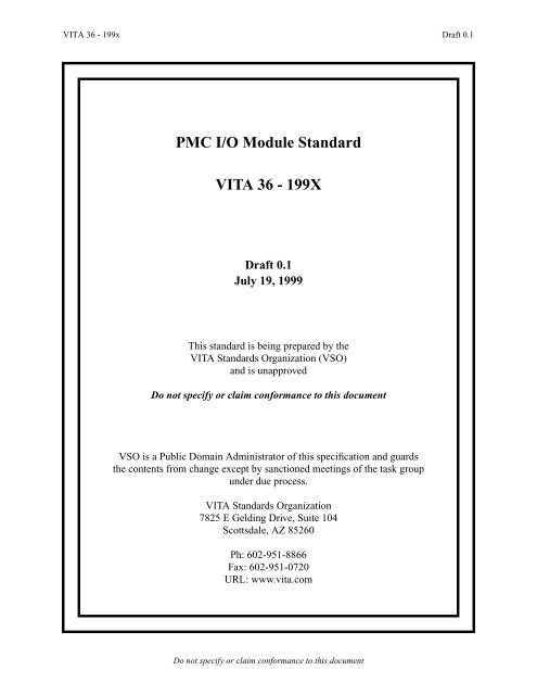
PMC I/O Module Standard VITA 36 - 199X
PMC I/O Module Standard VITA 36 - 199X
PMC I/O Module Standard VITA 36 - 199X

Create successful ePaper yourself
Turn your PDF publications into a flip-book with our unique Google optimized e-Paper software.
<strong>VITA</strong> <strong>36</strong> - 199x Draft 0.1<br />
<strong>PMC</strong> I/O <strong>Module</strong> <strong>Standard</strong><br />
<strong>VITA</strong> <strong>36</strong> - <strong>199X</strong><br />
Draft 0.1<br />
July 19, 1999<br />
This standard is being prepared by the<br />
<strong>VITA</strong> <strong>Standard</strong>s Organization (VSO)<br />
and is unapproved<br />
Do not specify or claim conformance to this document<br />
VSO is a Public Domain Administrator of this specification and guards<br />
the contents from change except by sanctioned meetings of the task group<br />
under due process.<br />
<strong>VITA</strong> <strong>Standard</strong>s Organization<br />
7825 E Gelding Drive, Suite 104<br />
Scottsdale, AZ 85260<br />
Ph: 602-951-8866<br />
Fax: 602-951-0720<br />
URL: www.vita.com<br />
Do not specify or claim conformance to this document
<strong>VITA</strong> <strong>36</strong> - 199x Draft 0.2<br />
1. Overview<br />
1.1 Scope<br />
This proposed standard defines a module intended to pair with a CMC compliant card via the 64<br />
I/O signals defined on the Pn4/Jn4 connectors. To the extent possible, the proposed module<br />
reuses mechanical dimensions, hardware and connector definitions set forth in the CMC specification.<br />
1.2 Purpose<br />
The CMC specification provides for user defined I/O to exit the CMC through one or more 64 pin<br />
connectors. This user I/O is commonly employed to bring I/O to the rear of the system in order to<br />
augment or replace the I/O available on the CMC’s bezel in the front of the system.<br />
One of the primary benefits of using a CMC is that functionality can be added at the system integration<br />
level as opposed to being designed in onto the host board. For applications in which CMC<br />
user I/O must be brought to connectors on the system panel, it is desirable to have a generic module<br />
to allow this aspect of the CMC’s functionality also to be integrated at the system level rather<br />
than the board level.<br />
1.3 General Arrangement<br />
The only current implementation of the CMC umbrella specification is the PCI Mezzanine Card<br />
(<strong>PMC</strong>). The definition of the <strong>PMC</strong> I/O <strong>Module</strong> (PIM) is based on their use on VME and CompactPCI<br />
transition boards. These transition boards hold similar form factors to their respective<br />
hosts with the exception of being shorter by 80mm. Consequently, the PIM is based on the standard<br />
length CMC but is 80mm shorter.<br />
There are two CMC style 64 pin connectors on the PIM. One connector is dedicated to the 64<br />
user I/O signals routed to it from the CMC. The second connector provides power and ground to<br />
the PIM. The second connector may also be used to bring host signals onto the PIM.<br />
1.4 Dimensions<br />
The intention is to reuse as much hardware and dimensional information as possible from the<br />
CMC specification. Stacking heights, connectors and bezel dimensions are unchanged from IEEE<br />
P1386. The CMC I/O envelope remains unchanged but the component envelope height limit is<br />
increased to better accommodate taller physical layer components (such as transformers, fuses,<br />
etc.).<br />
2. References<br />
The following publications are referenced within this document:<br />
[1] IEEE P1386 <strong>Standard</strong> Mechanics for a Common Mezzanine Card Family: CMC<br />
[2] IEEE P1386.1 <strong>Standard</strong> Physical and Environmental Layers for PCI Mezzanine Cards: <strong>PMC</strong><br />
Do not specify or claim conformance to this document 2 of 14
<strong>VITA</strong> <strong>36</strong> - 199x Draft 0.2<br />
3. Definitions, Abbreviations, and Terminology<br />
3.1 Special Word Usage<br />
Special word usage is unchanged from IEEE P1386.<br />
3.2 Definitions<br />
Host - refers to the board carrying the CMC.<br />
Carrier - refers to the board carrying the PIM. The host and the carrier may be the same board.<br />
Others definitions are unchanged from IEEE P1386.<br />
3.3 Abbreviations<br />
PIM - <strong>PMC</strong> I/O <strong>Module</strong><br />
Others abbreviations are unchanged from IEEE P1386.<br />
4. <strong>PMC</strong> I/O <strong>Module</strong> Mechanics<br />
4.1 PIM Size Designations and Sizes<br />
Two different PIM sizes are defined. These sizes are defined in Table 1.<br />
Table 1: PIM PCB Size Designations and Dimensions<br />
Designation Width Depth<br />
Single 74.0 69.0<br />
Double 149.0 69.0<br />
4.2 PIM Envelope<br />
One notable departure from the CMC specification is in the definition of the component envelope<br />
space on the PIM and the carrier. It is envisioned that PIMs will typically be located on transition<br />
or connector break-out boards. Such carriers do not typically have large numbers of electronic<br />
components. This is taken advantage of to provide more room on the PIM for tall components by<br />
reducing the space allotted to the carrier. Thus it may be possible to use physical interface components<br />
on the PIM which may not fit on the CMC itself.<br />
Note that the I/O envelope is identical to that on the CMC. This allows any connector arrangement<br />
on a CMC to be effortlessly replicated on the PIM.<br />
The envelopes for a PIM and its carrier are detailed in Figure 1.<br />
4.3 PIM Dimensions<br />
The mechanical dimensions of the single and double PIM sizes are given in Figure 2 and Figure 3<br />
respectively.<br />
Note that standoff hole size is not defined. The size of these holes depends on how the standoffs<br />
are permanently attached to the PIM during assembly.<br />
Do not specify or claim conformance to this document 3 of 14
<strong>VITA</strong> <strong>36</strong> - 199x Draft 0.2<br />
4.4 Connector Positioning, Orientation and Labeling<br />
The PIM has two EIA E700 AAAB connectors identical to those used on a CMC. Likewise, pad<br />
layout is the same as that specified for a CMC.<br />
It is expected that a PIM will normally have an orientation within a system opposite to that of its<br />
mating CMC. For instance, if a CMC is pointed bezel-wise towards the front of the system then<br />
the PIM will be pointing bezel-wise to the rear. To facilitate flow-through routing of the 64 user<br />
I/O signals, the Pn4 is moved to the opposite side of the PIM (to where Pn2 is located on a CMC)<br />
and is rotated by 180° from the orientation on the CMC. The label of Pn4 is kept to underscore<br />
the fact that it connected by the carrier and host to the Pn4 connector on the CMC.<br />
The other connector is labelled Pn0 to emphasize that its use has no corresponding function in the<br />
CMC Pn1 through Pn4 connectors.<br />
The relative positioning and orientation of the connectors on the PIM (and on the CMC for reference)<br />
are shown in Figure 4.<br />
4.5 Power Consumption and Dissipation<br />
Power drawn from the carrier shall not exceed the limits shown in Table 2. Under no circumstances<br />
should more than 0.5 amps be drawn through any single pin. The carrier should use<br />
bypass capacitors to ground on the PIM power pins.<br />
Table 2: PIM Allowable Power Dissipation (In Watts)<br />
Source Single Dual<br />
Total TBD TBD<br />
5V TBD TBD<br />
3.3V TBD TBD<br />
+12V TBD TBD<br />
-12V TBD TBD<br />
4.6 PIM Bezel and Stacking Heights<br />
PIM stacking heights and bezel are unchanged from the CMC definitions.<br />
Do not specify or claim conformance to this document 4 of 14
<strong>VITA</strong> <strong>36</strong> - 199x Draft 0.2<br />
Figure 1: Component Height Limits<br />
Do not specify or claim conformance to this document 5 of 14
<strong>VITA</strong> <strong>36</strong> - 199x Draft 0.2<br />
Figure 2: Single PIM<br />
Do not specify or claim conformance to this document 6 of 14
<strong>VITA</strong> <strong>36</strong> - 199x Draft 0.2<br />
Figure 3: Double PIM<br />
Do not specify or claim conformance to this document 7 of 14
<strong>VITA</strong> <strong>36</strong> - 199x Draft 0.2<br />
Figure 4: Positioning and Orientation of PIM Connectors<br />
1<br />
2<br />
Pn1<br />
Pn2<br />
<strong>PMC</strong><br />
Component Side<br />
1<br />
2<br />
Pn3<br />
Pn4<br />
63 1<br />
Pn0 Pn4<br />
64 2<br />
PIM<br />
Component Side<br />
Do not specify or claim conformance to this document 8 of 14<br />
63<br />
64<br />
63<br />
64
<strong>VITA</strong> <strong>36</strong> - 199x Draft 0.2<br />
5. Carrier PIM Slot Mechanics<br />
5.1 Carrier PCB Mechanics<br />
VME or CompactPCI carrier boards can supprt either one or two PIM slots. The mechanics of<br />
these PCBs are defined in Figure 5 and Figure 6 for one or two slots, respectively.<br />
5.2 Connectors<br />
All host PIM connectors shall use the EIA E700 AAAB connector as required in the CMC specification.<br />
These connectors shall be referred to as the receptacle, or “Jn” connector. For single slot<br />
carriers, the connectors are labeled J10 and J14. For two slot carriers, the connectors are labeled<br />
J10, J14, J20 and J24. The host is required to supply both connectors.<br />
Connector layout is the same as CMC, however position and orientation with regard to pin one<br />
location differs as shown in Figure 4.<br />
5.3 Carrier Front Panel Opening and Filler<br />
Size and placement of one or more PIM slot openings in the carrier front panel remain the same as<br />
the openings defined in the CMC specification. Consequently the PIM carrier may use filler panels<br />
used by CMC compliant hosts.<br />
Do not specify or claim conformance to this document 9 of 14
<strong>VITA</strong> <strong>36</strong> - 199x Draft 0.2<br />
Figure 5: VME or CompactPCI Carrier for Single PIM<br />
Do not specify or claim conformance to this document 10 of 14
<strong>VITA</strong> <strong>36</strong> - 199x Draft 0.2<br />
Figure 6: VME or CompactPCI Carrier for Double or Two Single PIMs<br />
Do not specify or claim conformance to this document 11 of 14
<strong>VITA</strong> <strong>36</strong> - 199x Draft 0.2<br />
6. Electrical and Logical Layers<br />
6.1 Connector Utilization<br />
There are two 64 pin connectors on the PIM. One connector (Pn4) is reserved for CMC I/O and is<br />
directly mapped to the Pn4 connector on the CMC with which the PIM is paired. The second connector<br />
(Pn0) supplies power and logic ground to the PIM, and may optionally be used to bring<br />
host I/O signals onto the PIM.<br />
The carrier is required to provide both connectors and to supply power and ground through the<br />
Jn0 connector as defined in Table 3. The carrier is not required to connect any of the signal pins<br />
on Jn0.<br />
6.1.1 CMC I/O Connector<br />
The Pn4/Jn4 connectors are referred to as CMC I/O connectors. The signals on the PIM Pn4 connector<br />
are directly mapped to the CMC Pn4 connector. This means Pn4-1 on the CMC is routed<br />
to Pn4-1 on the PIM, CMC Pn4-2 to PIM Pn4-2, and so forth up to Pn4-64. How these signals are<br />
used is determined entirely by the CMC and PIM design.<br />
Note the Pn4 connector is in a different position and orientation on the PIM than on the CMC.<br />
6.1.2 Host I/O Connector<br />
The presence of the PIM slot on the carrier may displace host I/O from the carrier front panel. If<br />
no CMC is installed on the host (or the CMC does not require the use of a PIM) then the PIM slot<br />
may be reclaimed for host I/O. To support this the carrier may connect I/O signals to the Jn0 connector.<br />
A PIM which supports special host I/O instead of CMC I/O may be referred to as a “host<br />
I/O module”. Whereas a PIM is expected to function in any PIM slot, a host I/O module will only<br />
function in a PIM slot with the special connections it requires.<br />
If the host I/O module includes the Pn4 connector, it must not make any connections to the pins to<br />
prevent contention with a CMC which may be installed on the host.<br />
6.2 PIM Connector Pinout<br />
The pin assignments and signal names required for the PIM are given in Table 3.<br />
Do not specify or claim conformance to this document 12 of 14
<strong>VITA</strong> <strong>36</strong> - 199x Draft 0.2<br />
Table 3: PIM Connector Pin Assignments<br />
Pn0/Jn0 Pn4/Jn4<br />
Pin Signal Name Signal Name Pin Pin Signal Name SignalName Pin<br />
1 Signal +12V 2 1 I/O I/O 2<br />
3 Signal Signal 4 3 I/O I/O 4<br />
5 +5V Signal 6 5 I/O I/O 6<br />
7 Signal Signal 8 7 I/O I/O 8<br />
9 Signal +3.3V 10 9 I/O I/O 10<br />
11 Signal Signal 12 11 I/O I/O 12<br />
13 GND Signal 14 13 I/O I/O 14<br />
15 Signal Signal 16 15 I/O I/O 16<br />
17 Signal GND 18 17 I/O I/O 18<br />
19 Signal Signal 20 19 I/O I/O 20<br />
21 +5V Signal 22 21 I/O I/O 22<br />
23 Signal Signal 24 23 I/O I/O 24<br />
25 Signal +3.3V 26 25 I/O I/O 26<br />
27 Signal Signal 28 27 I/O I/O 28<br />
29 GND Signal 30 29 I/O I/O 30<br />
31 Signal Signal 32 31 I/O I/O 32<br />
33 Signal GND 34 33 I/O I/O 34<br />
35 Signal Signal <strong>36</strong> 35 I/O I/O <strong>36</strong><br />
37 +5V Signal 38 37 I/O I/O 38<br />
39 Signal Signal 40 39 I/O I/O 40<br />
41 Signal +3.3V 42 41 I/O I/O 42<br />
43 Signal Signal 44 43 I/O I/O 44<br />
45 GND Signal 46 45 I/O I/O 46<br />
47 Signal Signal 48 47 I/O I/O 48<br />
49 Signal GND 50 49 I/O I/O 50<br />
51 Signal Signal 52 51 I/O I/O 52<br />
53 +5V Signal 54 53 I/O I/O 54<br />
55 Signal Signal 56 55 I/O I/O 56<br />
57 Signal +3.3V 58 57 I/O I/O 58<br />
59 Signal Signal 60 59 I/O I/O 60<br />
61 -12V Signal 62 61 I/O I/O 62<br />
63 Signal Signal 64 63 I/O I/O 64<br />
Do not specify or claim conformance to this document 13 of 14
<strong>VITA</strong> <strong>36</strong> - 199x Draft 0.2<br />
6.3 <strong>PMC</strong> I/O Signal Routing<br />
In general, the signals routed from the CMC Pn4 connector to the PIM Pn4 connector should be<br />
as short as possible, be approximately matched in length and have as few impedance mismatches<br />
as possible.<br />
For VME and CompactPCI systems, the carrier will map the PIM Jn4 connector onto the backplane<br />
connector(s) in the exact same manner as the host maps the CMC Jn4 connector onto the<br />
backplane connector(s).<br />
6.4 Host I/O Signal Routing<br />
Host I/O is specific to the host. It is expected that the manufacturer of the carrier will also manufacture<br />
any host I/O modules which may be accommodated by the carrier. Requirements for host<br />
I/O signal routing must be determined by that manufacturer.<br />
Higher speed signals should avoid using the +12V or -12V power pins as a signal return path.<br />
These power sources are generally not implemented with a plane and although it is recommended<br />
that the carrier bypass these voltages to ground near the connector, it is not required.<br />
Do not specify or claim conformance to this document 14 of 14