

LCD Module User Manual
LCD Module User Manual
LCD Module User Manual

Create successful ePaper yourself
Turn your PDF publications into a flip-book with our unique Google optimized e-Paper software.
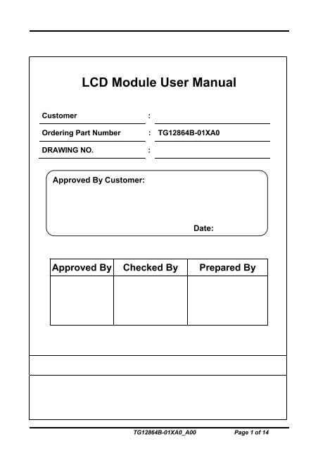
<strong>LCD</strong> <strong>Module</strong> <strong>User</strong> <strong>Manual</strong>Customer :Ordering Part Number: TG12864B-01XA0DRAWING NO. :Approved By Customer:Date:Approved By Checked By Prepared ByTG12864B-01XA0_A00 Page 1 of 14
Contents1. Precautions in Use of <strong>LCD</strong> <strong>Module</strong>-------------------------------------P32. General Specification-------------------------------------------------------P33. Absolute Maximum Ratings-----------------------------------------------P34. Electrical Characteristics--------------------------------------------------P45. Backlight Information------------------------------------------------------P46. Optical Characteristics-----------------------------------------------------P57. Interface Description--------------------------------------------------------P68. Contour Drawing & Block Diagram--------------------------------------P79. Application circuit----------------------------------------------------------P810. Timing Characteristics-------------------------------------------------P911. Display Control Instruction-------------------------------------------P1011.1 Instruction table----------------------------------------------------P1011.2 Instruction description --------------------------------------------P1012. Reset and Initializing flow chart --------------------------------------P1213. Display Data RAM map ------------------------------------------------P1314. Revision records------------------------------------------------------P14TG12864B-01XA0_A00 Page 2 of 14
1. Precautions in Use of <strong>LCD</strong> <strong>Module</strong>(1) Avoid applying excessive shocks to the module or making any alterations or modifications to it.(2) Don’t make extra holes on the printed circuit board, modify its shape or change the components of <strong>LCD</strong><strong>Module</strong>.(3) Don’t disassemble the LCM.(4) Don’t operate it above the absolute maximum rating.(5) Don’t drop, bend or twist LCM.(6) Soldering: only to the I/O terminals.(7) Storage: please storage in anti-static electricity container and clean environment.2. General SpecificationItem Standard Value UnitNumber of dots 128X64 Dots DotsOutline dimension 93.0(W)X70.0(H)X11.8MAX.(T) mmView area 71.8(W)X38.8(H) mmActive area 66.52(W)X33.24(H) mmDot size 0.48(W)X0.48(H) mmDot pitch 0.52(W)X0.52(H) mm<strong>LCD</strong> typeView directionBacklightSTN,Yellow-Green,Positive,Transflective6 o’clockSide LED, Yellow-Green3. Absolute Maximum RatingsITEM SYMBOL MIN. TYP. MAX. UNITOperating Temperature T OP -20 - +70 Storage Temperature T ST -30 - +80 Input Voltage V I 0 - V DD VSupply Voltage For Logic V DD 0 - 5.5 VSupply Voltage For <strong>LCD</strong> V DD -V EE 0 - 5 VTG12864B-01XA0_A00 Page 3 of 14
4. Electrical CharacteristicsITEM SYMBOL CONDITION MIN. TYP. MAX. UNITLogic Voltage V DD -V SS - 4.7 5.0 5.2 VSupply Voltage for <strong>LCD</strong> V DD -V O Ta=25 --- 9.0 --- VInput High Volt. V IH - 2.0 - V DD VInput Low Volt. V IL - -0.3 - 0.8 VOutput High Volt. V OH I oH =-0.2mA 2.4 - V DD VOutput Low Volt. V OL I oL =1.6mA 0 - 0.4 VSupply Current I DD(Include DC/DC) - --- 6.4 --- mA5. Backlight InformationAbsolute Maximum ratings (Ta=25)Item Symbol Conditions Rating UnitReverse voltage Vr - 5.0 VReverse Current Ir Vr=5.0V 80 uAAbsolute maximum forwardCurrentIfm 120mAPeak forward current Ifp I msec plus 10% Duty Cycle 240 mAPower dissipation Pd 340 mWOperating Temperature Range Toper -30~+70 Storage Temperature Range Tst -40~+80 Electrical/Optical Characteristics (Ta=25 0 C,If=80mA)ColorWavelengthp(nm)Spectral line halfwidth (nm)OperatingVoltage(v)(0.15V)ForwardCurrent (mA)Yellow-Green --- --- 3.1 80TG12864B-01XA0_A00 Page 4 of 14
6. Optical CharacteristicsITEM SYMBOL CONDITION MIN TYP MAX UNITView Angle(V) CR2 10 120 deg.(H) CR2 -45 45 deg.Contrast Ratio CR 5 Response TimeT rise 200 300 msT fall 150 200 msTG12864B-01XA0_A00 Page 5 of 14
7.Interface DescriptionPin No. Symbol Level Description1 V SS 0V Ground2 V DD 5.0V Power supply for Logic3 V O (Variable) Driving voltage for <strong>LCD</strong>4 RS H/L H:Data L :Instruction5 RW H/L H:Read L:Write6 E H/L Enable signal7~14 DB0~DB7 H/L Data bus. DB7 is used for Busy Flag .15 CS1 H Selection for IC1,active High16 CS2 H Selection for IC2,active High17 /RST L Reset signal, active low18 VEE -10V Negative voltage output19 A(LED+) +5.0V Anode of LED Backlight20 K(LED-) 0V Cathode of LED BacklightTG12864B-01XA0_A00 Page 6 of 14
8. Contour Drawing & Block DiagramTG12864B-01XA0_A00 Page 7 of 14
9. Application circuit8080-series MPU Circuit6800-series MPU CircuitTG12864B-01XA0_A00 Page 8 of 14
10. Timing CharacteristicsCharacteristic Symbol Min. Type Max. UnitE cycle t C 1000 nsE high level width t WH 450 nsE low level width t WL 450 nsE rise time t R 25 nsE fall time t F 25 nsAddress set -up time t ASU 140 nsAddress hold time t AH 10 nsData set -up time t DSU 200 nsData delay time t D 320 nsData hold time (write) t DHW 10 nsData hold time (read) t DHR 20 nsTG12864B-01XA0_A00 Page 9 of 14
11. Display Control InstructionThe display control instructions control the internal state of the TG12864B. Instruction isreceived from MPU to TG12864B for the display control. The following table shows variousinstructions.11.1 Instruction tableInstruction RS RW DB7 DB6 DB5 DB4 DB3 DB2 DB1 DB0 FunctionDisplayOn/offSet Address(Y address)Set Page(X address)DisplayStart LineStatusReadWriteDisplayDataReadDisplayData0 0 0 0 1 1 1 1 1 D0 0 0 1 Y address (0~63)0 0 1 0 1 1 1 Page (0~7)0 0 1 1 Display start line (0~63)0 1 Busy 0ON/OFFReset 0 0 0 01 0 Write data1 1 Read dataControls the display ON orOFF.The internal statusand the DDRAM data isnot affected.D=0: OFF; D=1: ONSets the Y address at thecolumn address counterSets the X address at theX address register.Indicates the Display DataRAM displayed at the topof the screen.Reads the internal statusBUSY0: Ready1: In operationON/OFF0: Display ON1: Display OFFRESET0: Normal1: ResetWrites data (DB[0:7]) intothe DDRAM. After writinginstruction, Y address isincriminated by 1automaticallyReads data (DB[0:7]) fromdisplay data RAM to thedata bus.11.2 Instruction Description1) Display On/OffThe display data appears when D is 1 and disappears when D is 0.Though the data is not on the screen with D=0, it remains in the display data RAM.Therefore,you can make it appear by changing D=0 into D=1.RS R/W DB7 DB6 DB5 DB4 DB3 DB2 DB1 DB00 0 0 0 1 1 1 1 1 DTG12864B-01XA0_A00 Page 10 of 14
2) Set Address (Y Address)Y address (AC0~AC5) of the display data RAM is set in the Y address counter.An address is set by instruction and increased by 1 automatically by read or writeoperations of display data.RS R/W DB7 DB6 DB5 DB4 DB3 DB2 DB1 DB00 0 0 1 AC5 AC4 AC3 AC2 AC1 AC03) Set Page (X Address)X address (AC0~AC2) of the display data RAM is set in the X address register.Writing or reading to or from MPU is executed in this specified page until the next page isset.RS R/W DB7 DB6 DB5 DB4 DB3 DB2 DB1 DB00 0 1 0 1 1 1 AC2 AC1 AC04) Display Start Line (Z Address)Z address (AC0~AC5) of the display data RAM is set in the display start line register anddisplayed at the top of the screen.When the display duty cycle is 1/64 or others (1/32~1/64), the data of total line number of<strong>LCD</strong> screen, from the line specified by display start line instruction, is displayed.RS R/W DB7 DB6 DB5 DB4 DB3 DB2 DB1 DB00 0 1 1 AC5 AC4 AC3 AC2 AC1 AC05) Status ReadRS R/W DB7 DB6 DB5 DB4 DB DB2 DB DB00 1 BUSY 0 ON/OFF RESET 0 0 0 0• BUSYWhen BUSY is 1, the Chip is executing internal operation and no instructions areaccepted.When BUSY is 0, the Chip is ready to accept any instructions.• ON/OFFWhen ON/OFF is 1, the display is off.When ON/OFF is 0, the display is on.• RESETWhen RESET is 1, the system is being initialized.In this condition,no instructionsexcept status read can be accepted.When RESET is 0, initializing has finished and the system is in the usual operationcondition.6) Write Display DataWrites data (D0~D7) into the display data RAM.After writing, Y address is increased by 1automatically.RS R/W DB7 DB6 DB5 DB4 DB3 DB2 DB1 DB01 0 D7 D6 D5 D4 D3 D2 D1 D07) Read Display DataReads data (D0~D7) from the display data RAM.After reading instruction, Y address is increased by 1 automatically.RS R/W DB7 DB6 DB5 DB4 DB3 DB2 DB1 DB01 1 D7 D6 D5 D4 D3 D2 D1 D0TG12864B-01XA0_A00 Page 11 of 14
12.Reset and Initializing flow chart12.1 ResetThe system can be initialized by setting RSTB terminal at low level when turning power on,receiving instruction from MPU.When RSTB becomes low, following procedure is occurred.Display offDisplay start line register become set by 0. (Z-address 0)While RSTB is low, No instruction except status read can be accepted. Therefore, executeother instructions after making sure that DB4 = 0 (clear RSTB) and DB7 = 0 (ready) bystatus read instruction. The Conditions of power supply at initial power up are shown asfollow.Item Symbol Min Typ Max UnitReset time t RS 1.0 - - uSRise time t R - - 200 nS12.2 Initializing flow chartPower onWait for more than 30mSSet Display Start Line to first lineRS RW D7 D6 D5 D4 D3 D2 D1 D00 0 1 1 0 0 0 0 0 0Set Display ONRS RW D7 D6 D5 D4 D3 D2 D1 D00 0 0 0 1 1 1 1 1 1Initialization EndTG12864B-01XA0_A00 Page 12 of 14
13. Display Data RAM mapTG12864B-01XA0_A00 Page 13 of 14
14. Revision recordsVersion Ref.pages Revision Items DateA00 All New release 2005.03.01TG12864B-01XA0_A00 Page 14 of 14