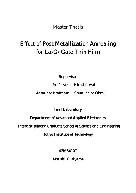
Effect of Post Metallization Annealing for La 2 O 3 Thin Film
Effect of Post Metallization Annealing for La 2 O 3 Thin Film
Effect of Post Metallization Annealing for La 2 O 3 Thin Film

You also want an ePaper? Increase the reach of your titles
YUMPU automatically turns print PDFs into web optimized ePapers that Google loves.
CONTENTSChapter 1 Introduction----------------------------------------------- 11.1 Background------------------------------------------------ --------------- 21.1.1 Background <strong>of</strong> This Study------------------------------------- 21.1.2 Limits <strong>of</strong> Silicon Dioxide (SiO2) as Gate Insulator ---- 41.1.3 Requirements <strong>for</strong> High-k Gate Dielectrics----------------61.2 Rare Earth Oxides as the Candidates <strong>of</strong> High-k Dielectricsand Their Properties-----------------------------------------------------81.3 Purpose <strong>of</strong> My Study---------------------------------------------------11Chapter 2Fabrication and Characterization Methods-----------132.1 Fabrication Methods--------------------------------------------------142.1.1 Wet Cleaning Method <strong>of</strong> Silicon Substrates----------152.1.2 Chemical Oxidation Treatment--------------------------162.1.3 Molecular Beam Deposition (MBD) Method----------172.1.4 Rapid Thermal <strong>Annealing</strong> (RTA) Method-------------192.1.5 Vacuum Evaporation Method-----------------------------212.2 Fabrication Methods <strong>of</strong> MIS Transistor-------------------------222.2.1 Capacitance-Voltage (C-V) Characteristics-----------222.2.2 Leakage Current Density-Voltage (J-V) Characteristics-------------272.2.3 Ellipsometry Method----------------------------------------29i
3.4.3 <strong>Effect</strong>s <strong>of</strong> PMA <strong>for</strong> Platinum Upper Electrodes------753.4.3.1 Dependence on the Temperature <strong>of</strong> PMA withPlatinum Upper Electrodes------------------------753.4.3.2 Dependence on the <strong>Annealing</strong> Time <strong>of</strong> PMAwith Platinum Upper Electrodes-----------------783.4.3.3 Dependence on the Ambience <strong>of</strong> PMA withPlatinum Upper Electrodes----------------------803.4.3.4 The Summary <strong>of</strong> This Section----------------------863.4.4 Examination <strong>of</strong> PMA <strong>for</strong> Another Rare Earth Oxide-----------88Chapter 4Conclusionsclusions-----------------------------------------------894.1 Summary <strong>of</strong> This Investigation--------------------------------------- 904.1.1 Summary <strong>of</strong> the investigation into the annealing withAluminum Upper Electrodes--------------------------------------- 904.1.2 Summary <strong>of</strong> the Investigation into the <strong>Annealing</strong> withGold Upper Electrodes---------------------------------------- 914.1.3 Summary <strong>of</strong> the Investigation into the <strong>Annealing</strong> withPlatinum Upper Electrodes----------------------------------914.1.4 Summary <strong>of</strong> the <strong>Effect</strong>s <strong>of</strong> PMA <strong>for</strong> Gd2O3 <strong>Thin</strong> <strong>Film</strong>swith Aluminum Upper Electrodes-------------------------924.2 Considerations about an Occurrence and a Recovery <strong>of</strong> VFBShift-------------------------------------------------------------------------944.3 Future Issues------------------------------------------------------------98Acknowledgements-------------------------------------------------------------99References-----------------------------------------------------------------------101iii
Chapter 1Introduction-1 -
1.1 BackgroundIn this section, the general perspective <strong>of</strong> the present semiconductortechnology and the background <strong>of</strong> this investigation will be described in thepages that follow.1.1.1 Background <strong>of</strong> This StudyIn recent years, a magnificent influence <strong>of</strong> silicon LSI technology hasappeared in a large number <strong>of</strong> scenes such as our social, business anddomestic lives, and that has supported essential part <strong>of</strong> them. The higherper<strong>for</strong>mance and the lower consumption power equipments using silicon LSItechnology like personal computers and cellular phones have been developedwith great <strong>for</strong>ce as shown in Figure 1-1. The principal element whichmakes it possible is the improvements <strong>of</strong> Metal-Oxide-Semiconductor Field<strong>Effect</strong> Transistor (MOS FET), especially by miniaturizing the physical size <strong>of</strong>the devices according to scaling method. Scaling method is the way <strong>of</strong>shrinking the devices with same factor S as shown in Figure 1-2 and Table1-1. To downsize the devices leads to high speed switching operation andlower power consumption owing to the shrink <strong>of</strong> the channel length, andwhole per<strong>for</strong>mance <strong>of</strong> LSI system also can becomes higher becauseminiaturizing the devices realizes to contain much higher number <strong>of</strong>transistor in the same area, which improve high-speed, high-frequencycharacteristics. Investigating the device <strong>for</strong> downsizing is hence farimportant and has continued throughout the world.Fig. 1-1: Trends <strong>of</strong> CPU Clock and RAM Size-2 -
Miniaturization with a scaling factor SX jWN DSourcet OXL gGateN DDrainGateSourceW’=W/SX j’=X /Sj L g’=LN /SgD’=N*S DDrain/S N D ’=NN At ox ’=t ox /SN A’=N*SA=N *SDFig. 1-2: Scaling Method on MOSFETTable 1-1: Scaling on MOSFET by a scaling factor SQuantityChannel lengthChannel WidthDevice AreaGate Oxide ThicknessGate CapacitancePer Unit AreaJunction DepthThreshold VoltageDoping Density(Acceptor)Doping Density(Donor)Be<strong>for</strong>eScalingL gWAt OXX jV thAfter ScalingL’ g = L/SW’ = W/SA’ = A/S 2t OX ’= t OX /SC OXC OX ’ = t OX *SX j ’= X j /SV th ’= V th /SN AN A ’ = N A *SN D N D ’ = N D *S-3 -
1.1.2 Limits <strong>of</strong> Silicon Dioxide (SiO2) ) as Gate InsulatorTo downsize the size <strong>of</strong> MOSFET, however, brings various difficultiesat the same time. One <strong>of</strong> them, considered as the decisive factor in future LSItechnology, is limits <strong>of</strong> SiO2 as gate insulator. As mentioned in <strong>for</strong>mersection, shrinking the devices has brought magnificent improvement in LSItechnology. At the mention <strong>of</strong> gate insulator, SiO2 had been used as gateinsulator since MOSFET was invented because SiO2 has good property suchas high stability with silicon substrate at high temperature process or lowdensity <strong>of</strong> fixed charge, defects in bulk and at the interface. Consequently,SiO2 had played a significant role <strong>of</strong> MOSFET and been downsized over along period <strong>of</strong> time.It is said recently, however, that <strong>Thin</strong>ning down SiO2 has beenreaching limits because <strong>of</strong> direct tunneling current. Table 1-2 shows theelectrical properties <strong>for</strong> 1 nm thickness SiO2 gate insulator. This table saysthat leakage current density reaches 100 A/cm 2 and, to make matters worse,when SiO2 thickness become below 0.8 nm, leakage current density willincrease over 1 kA/cm 2 caused by direct tunneling effect. Figure 1-3 showsthe schematic band diagram explaining direct tunneling mechanism. Incase <strong>of</strong> the thick insulator, that works as a barrier <strong>for</strong> carriers. There<strong>for</strong>e,leakage current remains low. In case <strong>of</strong> thin insulator, however, thequantum effect can not be negligible and carriers can get to pass through theinsulator directly. Consequently, leakage current becomes hugeexponentially. This undesirable effect will lead the increase <strong>of</strong> powerconsumption and degradation <strong>of</strong> LSI reliability and these unacceptablephenomena must be averted.Table 1-3 shows technology roadmap <strong>for</strong> various element <strong>of</strong> MOSFET.This roadmap indicates the value <strong>of</strong> EOT (Equivalent Oxide Thickness) willreach 0.9 nm in 2007 and 0.5 nm in 2016. However, it is said that practicalsolutions to realize EOT=0.9 nm are not known yet.From the <strong>for</strong>egoing, it is considered that revolutionary change to solvethese problems is strongly required and one <strong>of</strong> the answers is to replace SiO2to new material.-4 -
Table 1-2: Electrical Properties <strong>for</strong> 1nm thickness SiO2 Gate InsulatorEOT [nm] 1.0Leakage Current Density [A/cm2] 100Gate Length [0m( 0.1Gate Width [0m] 5Gate Area [cm2] 5 X 10 -9Functions per Chip (Transistors/Chip) 1 X 10 8Total Gate Area [cm 2 ] 5 X 10 -1Total Leakage Current per Chip [A/chip] 50V oxDirect TunnelingV gMetal SiO 2 n-SiFigure 1-3: The Schematic Band Diagram <strong>for</strong> <strong>Thin</strong> SiO2 MOS CapacitorTable 1-3: Projections <strong>of</strong> the sizes <strong>of</strong> MOSFETYear 2004 2007 2010 2013 2016Node [nm] 90 65 45 32 22Lg [nm] 37 25 18 13 9EOT [nm] 1.2 0.9 0.7 0.6 0.5Vdd [V] 1.2 1.1 1.0 0.9 0.8-5 -
1.1.3 Requirements <strong>for</strong> High-k Gate DielectricsThe reason to thin down SiO2 is to increase gate charges, whichincreases drain current. The capacitance Ci <strong>of</strong> gate dielectric at unit area isexpressed with the following equation,Cε kt0i= (1.1)where ε0and k are vacuum and relative dielectric constant, respectivelyand t is the thickness <strong>of</strong> gate dielectrics. The value <strong>of</strong> vacuum dielectricconstant is about 8.85× 10 −14 [F/cm] and relative dielectric constant <strong>of</strong> SiO2 is3.9. <strong>Thin</strong>ning down SiO2 used to be a simple and effective way to obtainhigh capacitance value as SiO2 is greatly stable with silicon substrates asmentioned in <strong>for</strong>mer section. Now that the limit <strong>of</strong> SiO2 is showing up,however, another way to increase the capacitance value is required. Theanswer <strong>for</strong> this requirement is to introduce new materials which have highdielectric constant. These materials are called high-k dielectrics. If onematerial which have a dielectric constant, k=7.8 (double compared to SiO2)can be replaced instead <strong>of</strong> SiO2, the capacitance value is maintained eventhough thickness <strong>of</strong> gate insulator become twice. If this replacement can bepossible, that will be the answer enough to prevent direct tunneling effecttaking place shown in Figure 1-4.It is, however, not simple to replace SiO2 to the high-k materials,because the high-k dielectrics must satisfy several conditions whichdetermine the electrical properties <strong>of</strong> MOSFET. The requirements <strong>for</strong>high-k dielectrics are described in the pages that follow.(1) High dielectric constantAs is already mentioned, the higher dielectric constant is, the thickerthe gate insulator can be <strong>for</strong> same capacitance value. At the same time,however, the band gap which determines the barrier height against electronsand holes is roughly inversely proportional to the dielectric constant.There<strong>for</strong>e, it is necessary <strong>for</strong> high-k dielectrics to be compatible with theband gap in order to suppress the leakage currents due to Schottky emission.Generally, it is considered that dielectric constant less than 50 is desirable.(2) Stability at high thermal condition in contact with Si surfaceThere are some processes with thermal condition around 1000K in-6 -
LSI fabrication, such as activation after impurity doping. During such athermal process, the <strong>for</strong>mation <strong>of</strong> SiO2 or MxSiyOz (silicate) may be grown atSi and high-k interface. These interfacial layers decrease the totaldielectric constant enormously. Recently, however, lots <strong>of</strong> investigatorshave reported that these Silicon-like material such as silicate or SiO2 layerproduce good properties in terms <strong>of</strong> mobility or leakage current density andthe attempt to use these layers positively is suggested.Furthermore, micro-crystal growth in the films may also occurduring the thermal process. That must be prevented because these conditionincrease leakage current tremendously.(3)Low densities <strong>of</strong> interface state, fixed charge and High mobilityMobility is one <strong>of</strong> the most important factors in properties <strong>of</strong>MOSFET because that directly affects the drain current. The key to obtainhigh mobility is the quality <strong>of</strong> the gate insulator. It is considered thatMobility is degraded by the carrier scattering effect caused by defects in thegate insulator such as fixed charges, which causes flat-band voltage shift,and higher density <strong>of</strong> interface states induce Coulomb scattering. Thesedefects in high-k films, hence, must be suppressed at a low level.From the mentioned above, the choice <strong>of</strong> high-k materials isexceedingly important and difficult as well. The representative materials <strong>of</strong>high-k dielectrics <strong>for</strong> gate insulator will be described in next section.V oxDirect TunnelingV ox High-kV gt SiO2Metal SiO 2 n-SiV gtMetalhigk − k =AtSiO 2n-Siε SiO 2 =3.9εSiO2CSiO=2tSiO2εSiO2EOT= =tCSiO2SiO2Chigh −kEOTεhigh − k =AεSiO 2high −k2= = =high −kFigure 1-4: Advantage <strong>of</strong> high-k materials to SiO2 as gate insulatorεtεSiOAεAtSiOSiOSiO22 2= = =Chigh −kεCSiO2CtSiOSiO22-7 -
1.2 Rare Earth Oxides as the Candidates <strong>of</strong> High-k Dielectricsand Their PropertiesIn order to overcome the limits <strong>of</strong> SiO2 explained in previous section,several promising materials have been investigated in recent years by alarge number <strong>of</strong> researchers. The elements which can be the candidates <strong>of</strong>the alternative insulator are quite limited because <strong>of</strong> the reaction failurewith Silicon or radioactivity as shown in Figure 1-5. Under these restrictedconditions, metal oxides (MOx) like Al2O3, ZrO , HfO2 and recently N, Si, orAl doped HfO2 gate dielectrics such as HfSiON, HfAlx, HfON and rare earthoxides have been studied eagerly <strong>for</strong> the next generation gate dielectricmaterials.Figure 1-5: Candidates <strong>of</strong> the elements which have possibility to be utilizedas high-k gate insulators-8 -
Table 1-4 shows the properties <strong>of</strong> the major candidate. SiO2 has thebiggest band gap and the highest barrier <strong>for</strong> electrons and holes, andremains amorphous in thermal condition through the LSI fabricationprocesses. Moreover, the contact stability with Silicon is completelyexcellent. Al2O3 has relatively higher band gap and remains amorphousagainst thermal processes. The dielectric constant, however, isconsiderably lower than other high-k candidates. ZrO2 and HfO2 used to beinvestigated much widely and zealously owing to their higher dielectricconstant. As the investigation steps ahead, however, several problems areshowing up. One <strong>of</strong> them is the <strong>for</strong>mation <strong>of</strong> interfacial layer, which makesEOT hugely increased, through the post deposition annealing processes.Another one is the crystallization at around 700 o C, which increases theleakage current tremendously. From these background, N, Si, or Al dopedHfO2 silicates have been reported frequently in very recent years.Rare earth oxides are considered as one <strong>of</strong> the most promising high-kmaterials because most <strong>of</strong> the rare earth oxides have the higher dielectricconstant on a level with ZrO2 or HfO2 and these metal oxides are relativelystable at the Silicon interface during the thermal process and it is reported toremain amorphous. Excellent results under EOT <strong>of</strong> 0.5 nm with lowerleakage current using rare earth oxides have also been reported.Table 1-4: Properties <strong>of</strong> major high-k materialsMaterials SiO 2 Al 2 O 3 <strong>La</strong> 2 O 3 Pr 2 O 3 Gd 2 O 3 HfO 2 ZrO 2EOT (nm) 0.8 1.5 0.48 1.4 1.5 0.8 0.8Contact stabilitywith Si (kJ/mol)Stable +63.4 +98.5 +105.8 +101.5 +47.6 +42.3Si+MO x →M+SiO 2<strong>La</strong>ttice energy(kJ/mol)13125 15916 12687 12938 13330 11188Bandgap (eV) 9 6 – 8 5.4 3.9 5.4 5.7 5.2 – 7.8Structure Amorphous Amorphous AmorphousCrystalCrystalCrystalCrystalT>400 -T>700ºCT>400ºCT>700ºC800ºCκ 3.9 8.5 – 10 27 13 17 24 11 – 18.5A. Chin et al., Symp. on VLSI Tech., pp. 16 - 17 (2000)-9 -
Figure 1-6 shows the candidates <strong>of</strong> rare earth materials <strong>for</strong> gateinsulators and their physical properties. Figure 1-6 (a) shows the value <strong>of</strong>band gap <strong>for</strong> rare earth oxides. This figure describes that each element hasutterly different value and <strong>La</strong>2O3, Gd2O3 and Lu2O3 has the highest band gap<strong>of</strong> 5.4 eV. And most <strong>of</strong> rare earth oxides have the enough value <strong>of</strong> band gaparound 5 eV. Figure 1-6 (b) shows the value lattice energy <strong>for</strong> rare earthoxides. <strong>La</strong>ttice energy means the energy which is required to separatesingle atom from the state <strong>of</strong> a crystal, namely the oxides having large latticeenergy tend to show easy crystallization. As shown in Figure 1-6 (b), thelattice energy <strong>of</strong> rare earth oxides become larger with an atomic number.Un<strong>for</strong>tunately, rare earth metal oxides also have several problems tobe a alternative replacement as the gate insulator. One <strong>of</strong> them is thepositive fixed charge in the rare earth oxides. This charge would make theflat band voltage (VFB) shift to negative side and degrade the mobility owingto Coulomb scattering as explained in <strong>for</strong>mer section. This unacceptableproblem must be solved in order to replace SiO2 <strong>for</strong> sub 100nm CMOStechnology.Candidates <strong>for</strong> gate insulator in Rare earth<strong>La</strong>CePrNdSmEuGdTbDyHoErTmYbLuBand Gap (eV)65432-14000Lu 2O Lu<strong>La</strong> 32O 2O3Gd 32 O 3 -13800Sm 2 O 3 Yb 2 O 3-13600Yb 2 O 3Dy 2O -13400 Gd 2 O Dy 2O 33 3Eu 2 O 3 Pr -132002O Sm 2O 33 Eu 2 O 3-13000Pr 2 O 3-12800<strong>La</strong> 2 O 3<strong>La</strong>ttice Energy (kJ/mol)-12600<strong>La</strong> 2 O 3 Pr 2 O 3 Sm 2 O 3 Gd 2 O 3 Dy 2 O 3 Er 2 O 3 Yb 2 O 3<strong>La</strong> 2 O 3 Pr 2 O 3 Sm 2 O 3 Gd 2 O 3 Dy 2 O 3 Er 2 O 3 Yb 2 O 3Ce 2 O 3 Nd 2 O 3 Eu 2 O 3 Tb 2 O 3 Ho 2 O 3 Tm 2 O 3 Lu 2 O 3 Ce 2 O 3 Nd 2 O 3 Eu 2 O 3 Tb 2 O 3 Ho 2 O 3 Tm 2 O 3 Lu 2 O 3Band Gap <strong>of</strong> Rare Earth Oxides<strong>La</strong>ttice Energy <strong>of</strong> Rare Earth OxidesFigure 1-6: Physical Properties <strong>of</strong> Rare Earth Oxides(a) Band Gap <strong>of</strong> Rare Earth Oxide (b) <strong>La</strong>ttice Energy <strong>of</strong> Rare Earth Oxides- 10 -
1.3 Purpose <strong>of</strong> My StudyIt is considered and concerned that one <strong>of</strong> the serious problems in all<strong>of</strong> high-k materials is the degradation <strong>of</strong> mobility. And one <strong>of</strong> the reasonswhy using high-k material degrades mobility is the fixed charges in high-kfilms as explained in <strong>for</strong>mer section. The fixed charges, moreover, wouldmake VFB shift and this effect would bring serious problems to electricalcharacteristics on MOSFET.Figure 1-7 shows that the C-V characteristics <strong>for</strong> MIS capacitor with<strong>La</strong>2O3 films fabricated by post deposition annealing (PDA) and as-deposition(no annealing), and ID-VD characteristics <strong>for</strong> MOSFET with <strong>La</strong>2O3 filmsfabricated by PDA process. From C-V characteristics shown in Figure 1-7(a), VFB shift toward negative side around -0.7V was observed despite <strong>of</strong>as-deposition. This result means that <strong>for</strong>med <strong>La</strong>2O3 thin films containpositive fixed charges in the state <strong>of</strong> as-deposition. Moreover, although theannealing process has a role as the improvement in electrical characteristics,a huge VFB shift more than 1V toward negative side was observed after PDAprocess. And it was also confirmed from ID-VD characteristics thatMOSFET with <strong>La</strong>2O3 thin films fabricated by PDA process has normally-oncharacteristics resulting from that enormous VFB shift. Normally-oncharacteristics on MOSFET would prevent from realizing the low powerconsumption.From the a<strong>for</strong>ementioned, this thesis focuses on the problem aboutVFB shift, and will report the results <strong>of</strong> another way <strong>of</strong> annealing, postmetallization annealing (PMA), and its optimization <strong>for</strong> rare earth oxides,mainly <strong>La</strong>2O3 thin films <strong>for</strong> the purpose <strong>of</strong> the suppression <strong>of</strong> VFB shift.-11 -
<strong>La</strong> 2 O 3PDA250 o C depo. HF-last(<strong>Post</strong> Deposition Anneal)235Al/<strong>La</strong> O / n-Si(100)/Al2 3 Lg/W = 2.5/27 µmPDA30250 o C depoas-depo.2520115Ideal V FB =-0.05V10V FB =-1.01V5Capacitance ( µF/cm 2 )0-1.5 -1 -0.5 0 0.5 1Voltage (V)Conventional anneal increases V FB shiftDrain Current I D (µA/µm)AlVg = 0.5 VVg = 0 V00 0.5 1 1.5 2 2.5 3Drain Voltage V (V)D Normally-ON characteristics on FETFigure 1-7: (a) C-V characteristics <strong>for</strong> Al/<strong>La</strong>2O3/n-Si(100)/Al MIS structuresfabricated by PDA process(b) ID-VD characteristics <strong>for</strong> MOSFET with <strong>La</strong>2O3 thin filmsfabricated by PDA process- 12 -
Chapter 2FabricationAndCharacterization Methods- 13 -
2.1 Fabrication MethodsThe electrical characteristics <strong>of</strong> rare earth oxide thin films were evaluated bymanufacturing Metal-Insulator-Semiconductor (MIS) capacitor. Thefabrication flow <strong>of</strong> MIS capacitors is shown in Figure 2-1. In thisinvestigation, two type <strong>of</strong> the annealing method were examined. One is<strong>Post</strong> Deposition <strong>Annealing</strong> (PDA) and another is <strong>Post</strong> <strong>Metallization</strong><strong>Annealing</strong> (PMA). In the pages that follow, each process will be described indetail.HF-last or Chemical Oxide (C.O.) treatment<strong>La</strong> 2 O 3 deposition (MBE) on n-Si(100)PDA[<strong>Post</strong> Deposition <strong>Annealing</strong>]upper electrode deposition (Al, Au or Pt)PMA[<strong>Post</strong> <strong>Metallization</strong> <strong>Annealing</strong>]back electrode deposition (Al)As-deposition PDA PDA+PMAPMAFigure 2-1: Fabrication Flow <strong>of</strong> MIS capacitors- 14 -
2.1.1 1 Wet Cleaning Method <strong>of</strong> Silicon SubstratesIt is well known that semiconductor science is highly sensitive tocontaminations or particles. These factors exert exceedingly on electricalcharacteristics. There<strong>for</strong>e, every process should be done with thorough care.On the basis <strong>of</strong> this fact, DI (de-ionized) water had been used through thecleaning <strong>of</strong> silicon substrates. DI water highly purified and filtered toremove all <strong>of</strong> ionic, particulate and bacterial contamination. Thetheoretical resistivity <strong>of</strong> pure water at 25 o C is 18.25 MΩcm. Ultra-purewater (UPW) systems used in this investigation provided UPW with morethan 18.2 MΩcm resistivity.The substrates were basically cleaned by RCA cleaning processproposed by W. kern et al in 1970. This is the wet cleaning method mainlyusing H2O2 and some chemical liquid. Figure 2-2 shows the steps used inmy investigations. Firstly, SPM cleaning was per<strong>for</strong>med in order to removeorganic materials and metal contaminations. SPM were made by mixing96% sulfuric acid (H2SO4) and 30% hydrogen peroxide (H2O2) and their ratiowas H2SO4:H2O2=4:1. And then, the native and/or chemical oxides wereremoved by 1% hydr<strong>of</strong>luoric acid (HF). Finally, the cleaned substrates weredipped in DI water <strong>for</strong> an instant. The surfaces <strong>of</strong> substrates result inhydrogen-terminated which are hydrophobic and tolerant <strong>of</strong> oxidationsbecause Si-H protect oxygen absorption. This cleaning is called HF-last.Dip in UPW <strong>for</strong> 10 minuteswith pouring continuouslyDip in SPM <strong>for</strong> 5 minutesDip in UPW <strong>for</strong> 10 minuteswith pouring continuouslyDip in 1% HF <strong>for</strong> 5 minutesDip in UPW <strong>for</strong> an instantFigure 2-2: Wet cleaning <strong>of</strong> silicon substrates- 15 -
2.1.2 Chemical Oxidation TreatmentChemical oxidation treatment on silicon surface is considered as thefine way to obtain the good surface condition and suppress the leakagecurrent. In order to compare with HF-last and investigate the effects <strong>of</strong>them, some <strong>of</strong> substrates were chemically oxidized by the following processas shown in Figure 2-3.After HF-last treatment, some <strong>of</strong> substrates were dipped in H2O2 anddipped in UPW <strong>for</strong> an instant.HF-last treatmentDip in H 2 O 2 <strong>for</strong> 30 minutesDip in UPW <strong>for</strong> an instantN 2 blowFigure 2-3: Chemical oxidation treatment- 16 -
2.1.3 Molecular Beam Deposition (MBD) MethodIn this investigation, MBD method using molecular beam epitaxy(MBE) equipment is introduced <strong>for</strong> rare earth oxides deposition.Depositions <strong>of</strong> rare earth oxides thin films were per<strong>for</strong>med on siliconsubstrates by using E-beam. The pressure in the MBE chamber duringdepositions was 10 -7 ~10 -5 Pa (10 -9 ~10 -7 Torr). Molecular beam is the onlymethod <strong>for</strong> the deposition in ultra high vacuum. MBD method has theadvantage <strong>of</strong> the lower contaminations and damage than other method suchas sputtering or Chemical Vapor Deposition (CVD). Accordingly, it can besaid that MBD method is suitable <strong>for</strong> research in basic characteristics <strong>of</strong> thinfilms.Figure 2-4 shows the schematic illustration <strong>of</strong> MBE equipment usedin this investigation. There are two vacuum chambers. One is loadingchamber where cleaned silicon substrates were loaded and growth chamber.There are four pumps, Turbo-Molecular Pump (TMP) and Rotary Pump (RP)in loading chamber, Titanium Sublimation Pump (TSP) and Ion Pump (IP) ingrowth chamber. There are also four E-guns and targets, and two powersupplies in order to be capable to evaporate two materials in the same time.E-gun acceleration <strong>of</strong> -5 kV were used in this investigation. The purity <strong>of</strong>99.999% <strong>La</strong>2O3 target was used in this investigation. The silicon substrateswere rotated during the deposition <strong>for</strong> the purpose <strong>of</strong> uni<strong>for</strong>mity <strong>of</strong> filmthickness. The film thickness during deposition was monitored with theInficon crystal oscillator sensor. In-situ RHEED system was equipped <strong>for</strong>crystallinity analysis at the silicon surface, and quadrupole gas analyzer wasalso equipped <strong>for</strong> the analysis <strong>of</strong> the gas in the growth chamber. Themeasurement <strong>of</strong> this gas detection is based on the mass spectrometry andsome peaks are usually observed at 2, 18, 28, 44 <strong>of</strong> molecule mass. Thesepeaks are considered to indicate H2, H2O, N2 and CO2. And the intensityratio was about 50:1:3:1. During the heating Silicon substrates, theintensity <strong>of</strong> H2O was slightly higher than that <strong>of</strong> CO2 and during deposition,this magnitude relation were reversed.- 17 -
Deposition Ch.Transfer rodTSPSubstratesOxidetargetLoadingCh.TMPBack pressure:~10 -10 TorrDuring deposition:~10 -9 ~10 -7 TorrIPE-gunRPDeposition rate:0.1~1 nm/minWafer size:3 inch availableFigure 2-4: The schematic illustration <strong>of</strong> MBE equipment- 18 -
2.1.4 Rapid Thermal <strong>Annealing</strong> (RTA) MethodIn order to obtain high quality films, annealing process afterdeposition is required. The annealing after deposition is considered to bringthe suppression <strong>of</strong> leakage current because <strong>of</strong> the defects in the films andsurface roughness. And this thermal process also exerts an influence onhysteresis and flat band voltage (VFB).The equipment <strong>for</strong> annealing used in this investigation wasMILA-3000 (ULVAC Co. Ltd). Figure 2-5 shows the schematic illustration<strong>of</strong> RTA equipment. The annealing was per<strong>for</strong>med by four infrared lampssurrounding the sample stage which were made <strong>of</strong> carbon and coated by SiC.The heating temperature was controlled by thermocouple feedback. Therate <strong>of</strong> raising temperature was per<strong>for</strong>med at 400 o C per a minute <strong>for</strong> allsamples in my investigation. As the ambience during the annealing,nitrogen, oxygen and <strong>for</strong>ming gas (F/G) in atmospheric pressure wereinvestigated respectively. And in order to remove the atmospheric impurityand improve the purity <strong>of</strong> the annealing ambience, the displacement <strong>of</strong> thegas ambience was per<strong>for</strong>med by rotations <strong>of</strong> two processes, filling up andexhausting mutually five times each annealing as shown in Figure 2-6.Exhausting process was per<strong>for</strong>med by rotary pump vacuuming <strong>for</strong> 30seconds at each time. The gas was flowing throughout the annealing withthe rate <strong>of</strong> 1.2 little per minute.Infrared <strong>La</strong>mpsRPExhaustSamplesSample StageN 2 O 2 F/GNeedle valveFlow MeterMain ValveInfrared <strong>La</strong>mpsThermocoupleFigure 2-5: RTA equipment- 19 -
An insertion <strong>of</strong> samplesEvacuation by RP <strong>for</strong> 1 minuteFilling up the gas up to atmospheric pressureEvacuation by RP <strong>for</strong> 30 seconds5 times rotationAfter 5 times rotation<strong>Annealing</strong> with flowing gas at the rate <strong>of</strong> 1.2 l/min.Figure 2-6: The procedure <strong>of</strong> RTA- 20 -
2.1.5 Vacuum Evaporation MethodAluminum, gold and platinum upper electrodes and backsidealuminum electrodes were deposited by vacuum evaporation equipment.The advantage <strong>of</strong> this method is the simplicity and the quickness <strong>of</strong>evaporation as compared with sputtering.Figure 2-7 shows the illustration <strong>of</strong> the vacuum evaporationequipment. In high vacuum chamber approximately 10 -5 Torr, metal sourcewas deposited on the samples through the metal shadow mask by thermalheating with high voltage regarding to aluminum and gold upper electrodes.In the case the deposition <strong>of</strong> platinum upper electrodes, E-gun beam wasused <strong>for</strong> evaporation because <strong>of</strong> its higher melting point. The meltingpoints <strong>of</strong> aluminum, gold and platinum melting are about 660 o C, 1063 o C,1776 o C respectively. The size <strong>of</strong> upper electrodes was about 110 µm indiameter. With regard to backside electrodes, aluminum was depositedwithout the mask after removing the native oxide on the silicon surface atbackside.Tungsten FilamentAlAuSampleMetal MaskSamplePtE-gunFigure 2-7: Vacuum evaporation method- 21 -
2.2 Characterization MethodsIn this section, the methods <strong>for</strong> characterization <strong>of</strong> MIS capacitors will bedescribed in pages that follow.2.2.1 Capacitance-Voltage (C-V) CharacteristicsC-V characteristics were obtained by using Precision LCR Meter (HP4284A, Agilent) to measure the MIS capacitor’s impedance as RC seriescircuit. The high-frequency from 10 kHz to 1MHz voltage, whose amplitudewas 20 mV, was applied on the d.c. voltage <strong>for</strong> bias.Figure 2-8 shows the ideal high-frequency C-V characteristics <strong>of</strong>n-type Si MIS capacitor. The ideal equivalent circuit is composed <strong>of</strong> a seriescapacitance <strong>of</strong> insulator component, Cinsulator and silicon surface component,Cs. When positive bias is applied to the metal side, it is called accumulationregion. There is no current flow in the structure in the case <strong>of</strong> an ideal MIScapacitor. There<strong>for</strong>e, voltage causes band bending at silicon surface andaccumulation <strong>of</strong> majority carriers (electrons). This is the reason that thiscase is called accumulation. Total capacitance in unit area <strong>of</strong> C isindependent on applied voltage and given byC C insulatorε εt0 r= = , (2.1)where ε0and ε rare vacuum and relative dielectric constant, respectivelyand t is the thickness <strong>of</strong> the insulator. The value <strong>of</strong> vacuum dielectricconstant is about 8.85× 10 −14 [F/cm]. C decreases near zero bias becausebroadening <strong>of</strong> accumulation charge causes series capacitance.When zero bias is applied and surface potential is zero, MIS capacitoris in flat band condition. Silicon surface capacitance <strong>of</strong> Cs is not zero andgiven byεε0 rNdCsfb= q , (2.2)kT−1923where q= 1.6× 10 C is the electronic charge, k = 1.38× 10 − J / K isBoltzmann’s constant, T is the absolute temperature and Nd is the density <strong>of</strong>ionized donors. From these equations, flat band capacitance <strong>of</strong> Cfb isobtained as following equation,- 22 -
1 1 1 t 1 kTC = C + C = εε+ q εεN. (2.3)fb insulator sfb 0 r 0 r dWhen a small negative voltage is applied, surface band bend upwardand apart from Felmi level. This is the state <strong>of</strong> depletion because majoritycarriers are depleted at the silicon surface. C keeps decreasing becausedepletion region act as a dielectric in series with the insulator.When a larger negative voltage is applied, the bands bend even moreupward such that the intrinsic level at the surface crosses over the Felmilevel. At this point, the number <strong>of</strong> holes (minority carriers) at surface islarger than that <strong>of</strong> holes, in other words, surface is inverted. Consequently,this state is called inversion. The total capacitance gets to a minimumbecause <strong>of</strong> following two reasons. Firstly, the recombination and generationrates <strong>of</strong> holes can not catch up with higher frequency signals. Fromempirical knowledge, it is possible <strong>for</strong> Metal-SiO2-Si MOS capacitor toincrease total capacitance up to the insulator capacitance again at the lowfrequency between 5 and 100 Hz. Secondly, once strong inversion occurs,the depletion layer width reaches a maximum because the semiconductor iseffectively shielded by further penetration <strong>of</strong> electric field by the inversionlayer. Accordingly, the maximum width, Wm, <strong>of</strong> the surface depletion regioncan be obtained as following equation,Wdm4εεkT ln( N / n )= , (2.4)o r a i2qNdwhere ni is intrinsic doping concentration. And the corresponding totalcapacitance is given byεoεr εoεrCmin= = . (2.5)t WmIn fact, flat band voltage, VFB, is not zero because there is the difference <strong>of</strong>work function between metal and semiconductor.In a practical MOS capacitor, interface traps and oxide charges exist andthese affect the ideal MOS characteristics. The influence <strong>of</strong> these chargesin the SiO2 and at SiO2/Si interface has been investigated extensively. Ithas not been understood at present if these theories can apply to high-k films.Here, only two type <strong>of</strong> factors, charges and traps is considered now.Charges in the dielectrics are called the fixed charge Qf, and it can not be- 23 -
charged or discharged over a wide variation <strong>of</strong> applied gate voltage. Thefixed charge density Qf is located near the high-k/Si interface and its origin isconsidered as excess silicon (trivalent silicon) or a loss <strong>of</strong> electrons fromexcess oxygen centers (non-bridging oxygen) near the high-k/Si interface.This positive Qf causes the C-V curve to shift toward negative side from theideal C-V curve <strong>for</strong> both n-type and p-type substrates. The magnitude <strong>of</strong>the shift is generally evaluated by the difference between experimental VFBand ideal VFB.CapacitanceC insulatorC FBInversionDepletionC minAccumulationVoltageFigure 2-8: The ideal high-frequency C-V curve <strong>of</strong> n-type Si MIS capacitor.- 24 -
In C-V curve, the two type <strong>of</strong> hysteresis exists in dependence on itsdirection. One is the charge injection type, and another is mobile ion typeas shown in Figure 2-9 and 2-10 respecticely. Verifying the type <strong>of</strong>hysteresis is greatly important to understand the conditions <strong>of</strong> films.At a Silicon surface, there are some located states <strong>of</strong> energy in the<strong>for</strong>bidden energy gap <strong>of</strong> silicon because the lattice <strong>of</strong> bulk silicon and all theproperties associated with its periodicity result in a termination. Theseinterface states capture some charges when the surface potential bendupward in the case <strong>of</strong> n-type silicon, and these interface states are locatedunder the Felmi level. The amount <strong>of</strong> trapped charges is consequentlyvaried by the applied voltage. The C-V curve, hence, does not shift toparallel direction compared to the ideal C-V curve. Trapped charges dependon the measured frequency because these trapping or releasing can notfollow the ac voltage swing. These trapped charges affect not only C-Vcharacteristics, but also MISFET characteristics. Surface states reduce theconduction current in MISFET. Furthermore, the trapped electrons andholes located at the interface can act as charged scattering centers <strong>for</strong> themobile carriers in a surface channel, and thus that could lead lower mobility.Interface states can also act as localized generation-recombination centers.These could lead to generation-recombination leakage currents and affectthe dielectric reliability.- 25 -
MetaltdSiV G+xxr:Charge DensityPotential by Mobile Ion :xρ( x)/εε0ρ( x)When this potential is canceled by gate voltage:∆ VG+ x=0,εε0where∆V GIs Gate Voltagetd ρ( x) 1 tdxWhen mobile ion is distributedV G=− xdx =−ρ( x)dx0 εε00C0tdthrough the films, total voltageεεwhich is required to cancel0whereC0=potential by mobile ion istdt Integral part result in charge anddxQIC= ρ( x ) dx,0which depend on xit is defined as Q ICt<strong>Effect</strong> <strong>of</strong> mobile ion charge maximumwhen mobile ion is on x=t d , andMinimum when mobile ion is on x=0Moreover, Coulomb interaction existBetween mobile charge and gate voltageV G 0(b)++++Metal+SiMetal+Si++No influence <strong>of</strong> mobile chargeFigure 2-9: The mechanism <strong>of</strong> mobile-ion-type hysteresisdCapacitance (µF/cm 2 )Maximum influence <strong>of</strong> mobile chargeVg0MetalMetal321(b)(a)0-2 -1 0 1 2Voltage (V)SiO 2Depletion <strong>La</strong>yerSiO 2e -n-Sie -When gate voltage is from negative side to 0Repulsion against an electronNo infection into oxide filmsn-SiWhen gate voltage is increased,An electron is drawn in oxide filmsIt Work as a negative charge in oxide filmsC-V curve remains normalCapacitance (µF/cm 2 )321C-V curve shifts to positive side0-2 -1 0 1 2Voltage (V)Figure 2-10: The mechanism <strong>of</strong> charge-injection-type hysteresis- 26 -
2.2.2 Leakage Current Density-Voltage (J-V) CharacteristicsJ-V characteristics <strong>for</strong> MIS capacitor were measured by PrecisionSemiconductor Parameter Analyzer (HP4156C, Agilent). In the case <strong>of</strong>ideal MIS capacitor, the conductance <strong>of</strong> the insulator is supposed to be zero.In fact, however, practical insulators show the carrier conduction byelectrons and holes when the electric field or temperature is sufficiently high.The two types <strong>of</strong> conduction models will be described here.Firstly, Poole-Frenkel model is due to field-enhanced thermalexcitation <strong>of</strong> trapped electrons into the conduction band as shown in Figure2-11. This is called trap-assist conduction. The expression <strong>of</strong>Poole-Frenkel emission is given by( βPFE −ΦPF)qJ = Joexp , (2.6) kTwhere J0( J0~ E ) is the low-field current density, ΦPFis the barrier height<strong>for</strong> Poole-Frenkel mechanism and βPFfield lowering coefficients are givenbyβPF3q= (2.7)πε ε0rA plot <strong>of</strong> ln(J/E) versus E 1/2 yields a straight line with a slope determined bydielectric constant <strong>of</strong> the insulator and the plot segment contains thein<strong>for</strong>mation <strong>of</strong> the barrier height as trapped charge in the insulator. Thisconduction process also has temperature dependence and J versus 1/T alsoyields a straight line.Secondly, Fowler-Nordheim model is one <strong>of</strong> the tunneling emissionscaused by the tunneling <strong>of</strong> trapped electrons into the insulator conductionband as shown in Figure 2-12. The expression is given byJFN3 23/2qE 4 2 m*Φ oxFN= exp2−, (2.8)16πΦ FN3 qE ox where Eoxis the electric field in the insulator and ΦFNis the barrier height<strong>for</strong> Fowler-Nordheim mechanism. Equation (2.8) shows thatFowler-Nordheim tunneling current is characterized by a straight line in a- 27 -
plot <strong>of</strong>2oxln( J / E ) versus 1/ Eox. The Fowler-Nordheim tunneling emissionhas the strongest dependence on the applied voltage but is essentiallyindependent on the temperature. These plots and/or temperaturedependence thus decide the carrier transport type.V oxΦ PFE cE vMetal Oxides p-SiliconE cE vFigure 2-11: Poole-Frenkel mechanismV oxΦFNE cE vMetal Oxides p-SiliconE cE vFigure 2-12: Fowler-Nordheim mechanism- 28 -
2.2.3 Ellipsometry MethodEllipsometry method was utilized <strong>for</strong> estimating the thickness <strong>of</strong> thedeposited rare earth film. The principle <strong>of</strong> ellipsometry method is to makeuse <strong>of</strong> the difference <strong>of</strong> polarization be<strong>for</strong>e and after reflection. Figure 2-13shows the plane-polarized light incident on a plane surface. The incidentpolarized light can be resolved into a component p, parallel to the plane <strong>of</strong>incidence and a component s, perpendicular to the plane <strong>of</strong> incidence. Thelight propagates as a fluctuation in electric and magnetic fields at rightangles to the direction <strong>of</strong> propagation. The reflection coefficientsEP( reflected)R = PE ( incident)(2.9)RSP= ES( reflected)E ( incident)(2.10)Sare not separately measurable. However, the complex reflection ratio ρdefined in terms <strong>of</strong> the reflection coefficients RP and RS or ellipsometricangles ψ and ∆,R P Sρ = = tan( ψ) ej∆(2.11)Ris measurable. Then, ψ and ∆ are called ellipso parameter.For the air (n0)-thin film (n1)-substrate (n2-jk2) system, where nx is the index<strong>of</strong> refraction and kx is the index <strong>of</strong> extinction coefficient. In the case <strong>of</strong>silicon substrate, n2 and k2 are known, then n1 and film thickness can becalculated from the result <strong>of</strong> ψ and ∆ measurement.Incident lightDeflectionE pE sψE pDetectorE sAmbience:n 0d 1<strong>Film</strong>:n 1Substrate:n 2Figure 2-13 Principle <strong>of</strong> ellipsometry method- 29 -
Chapter 3Experimental Results- 30 -
3.1 IntroductionIn this chapter, the results <strong>of</strong> post metallization annealing (PMA) <strong>for</strong>lanthanum oxides (<strong>La</strong>2O3) with several upper metal electrodes <strong>for</strong> thepurpose <strong>of</strong> the suppression <strong>of</strong> VFB shift will be reported. As upper metalelectrodes, aluminum, gold and platinum were investigated.3.2 Experimental ProcedureFigure 3-1 shows experimental procedure <strong>for</strong> MIS capacitors. Rareearth metal oxides were deposited on n-Si(100) substrates by ultra highvacuum e-beam deposition method. The pressure in the MBE chamberduring depositions was 10 -7 – 10 -5 Pa (10 -9 – 10 -7 Torr). E-beam depositionmethod has some advantages compared to conventional CVD or sputtering interms <strong>of</strong> purity and damage in the deposited films, respectively.Chemically cleaned N-type silicon (100) substrates were immediatelyloaded into the chamber. In this study, two surface pretreatments wereinvestigated. One is HF-last treatment and another is chemical oxidations,which are explained in chapter 2 respectively.Amorphous <strong>La</strong>2O3 thin films were deposited on silicon substrate byMBE system at 250 o C. The deposition rates <strong>of</strong> the films were 0.1-1.0nm/min.Some <strong>of</strong> the samples were annealed in N2, O2 or <strong>for</strong>ming gas ambiencefrom 0 second (spike) to 100 minutes by RTA (Rapid Thermal <strong>Annealing</strong>)system, be<strong>for</strong>e upper metal electrodes deposition. This annealing is namedas post deposition annealing (PDA).Upper electrodes were deposited through a metal hard mask. Some<strong>of</strong> the PDA samples and the other samples were annealed after the upperelectrodes deposition. This annealing is named as post metallizationannealing (PMA). In this study, aluminum, gold and platinum wereinvestigated as upper metal electrodes <strong>for</strong> PMA.Finally, back side Al electrodes were deposited <strong>for</strong> all the samples.The ratio <strong>of</strong> rising annealing temperature was investigated in the case<strong>of</strong> 75 o C/minute and 400 o C/minute about aluminum upper electrodes, andgold and platinum were investigated at annealing ratio <strong>of</strong> 400 o C/minute.- 31 -
<strong>Annealing</strong> temperature from 200 o C to 450 o C was investigated withregard to aluminum upper electrodes, from 300 o C to 450 o C was investigatedwith regard to gold upper electrodes and from 300 o C to 600 o C wasinvestigated in regard with platinum upper electrodes respectively.These fabricated MIS capacitors were characterized by C-V and J-V.MetalPDAPMAn-Si(100)Si Resistivity:0.02 - 0.8[Ω・m]Thickness:3~6 [nm]<strong>La</strong> 2 O 3 DepositionAt 250 o C<strong>La</strong> 2 O 3Temperature:200 o C~450 o CTime:Spike~100 minutes<strong>La</strong> 2 O 3Ambience:N 2 , O 2 or F/GMetal Material:•Aluminum•Gold•PlatinumTemperature:200 o C~600 o CTime:Spike~100 minutesAmbience:N 2 , O 2 or F/GMetalAlWet CleaningandSurface Treatment•HF-last•Chemical OxidationRare Earth Deposition(MBE)•PDA<strong>Annealing</strong> Process (RTA)•PMAUpper Metal Evaporation•PDAUpper Metal EvaporationPMA<strong>Annealing</strong> Process (RTA)Figure 3-1: The Fabrication Process <strong>for</strong> MIS Capacitors- 32 -
3.3 Electrical Characteristics in the case <strong>of</strong> PDABe<strong>for</strong>e the examinations <strong>of</strong> PMA, investigating the effects <strong>of</strong> PDAmust be done be<strong>for</strong>ehand. The following is the results <strong>of</strong> PDA.3.3.1 Dependence on the Temperature <strong>of</strong> PDAFigure 3-2 shows the C-V characteristics dependent on thetemperature <strong>of</strong> PDA <strong>for</strong> <strong>La</strong>2O3 thin films. The surface treatment wasHF-last and the annealing temperatures from 300 o C to 450 o C were examinedrespectively, and all <strong>of</strong> them were annealed <strong>for</strong> 10 minutes in nitrogenambience and measured at 1 MHz.The hysteresis was not observed both as-deposited samples and PDAsamples. That means <strong>La</strong>2O3 films have good properties without mobilecharges like K + or Na + ion and with few charge traps at the state <strong>of</strong>as-deposition. Moreover, it should be noted that the capacitance valueincreased with increase in the annealing temperature. This phenomenonsuggests two effects. One <strong>of</strong> them is that <strong>La</strong>2O3 films were densified by thehigher temperature annealing and their quality improved significantly.Another one is that high purity nitrogen ambient suppressed the growth <strong>of</strong>interfacial layer. On the other hand, however, it was found that the value <strong>of</strong>VFB shift increased with increase in the annealing temperature.Figure 3-3 shows the J-V characteristics dependence on thetemperature <strong>of</strong> PDA <strong>for</strong> <strong>La</strong>2O3 thin films. The annealing temperatures from300 o C to 450 o C were examined respectively. It was also found that leakagecurrent decreased with increase in the annealing temperature. This resultsuggests that the higher temperature post deposition annealing decreasedthe defects in <strong>La</strong>2O3 films.Figure 3-4 shows the frequency dependence on C-V characteristics <strong>of</strong>an as-deposited sample and PDA samples annealed at 300 o C, 400 o C and450 o C respectively. Ranges <strong>of</strong> frequency <strong>for</strong>m 10 kHz to 1 MHz weremeasured. It was observed that the fluctuations <strong>of</strong> measuring value werealmost completely suppressed by PDA at 450 o C.- 33 -
From the above mentioned, it can be concluded that post depositionannealing improved the electrical characteristics such as the capacitancevalue, leakage current, frequency dependence except <strong>for</strong> VFB shift towardnegative side.Al/<strong>La</strong> O / n-Si(100)/Al2 3Capacitance (µF/cm 2 )2250 o C depo. HF-lastAs-depo. & PDA300 o C to 450 o C10min.N ambient21450 o C400 o C300 o Cas-depo.Ideal V FB0-1.5 -1 -0.5 0 0.5Voltage (V)Figure 3-2: C-V characteristics dependent on temperature <strong>of</strong> PDA processCurrent Density (A/cm 2 )10 010 -210 -410 -610 2 -1 -0.5 0 0.5 1as-depo.300 o C400 o C450 o CAl/<strong>La</strong> O / n-Si(100)/Al2 3 250 o C depo. HF-last As-depo. & PDA300 o C to 450 o C 10min.N ambience210 -8Voltage (V)Figure 3-3: J-V characteristics dependent on temperature <strong>of</strong> PDA process- 34 -
Capacitance (µF/cm 2 )21Al/<strong>La</strong> O / n-Si(100)/Al2 3 250 o C depo. HF-lastAs-depo.10kHz to 1MHz10kHzCapacitance (µF/cm 2 )21Al/<strong>La</strong> O / n-Si(100)/Al2 3 250 o C depo. HF-lastPDA 300 o C 10min.N ambience2 10kHz to 1MHz10kHz0-1.5 -1 -0.5 0 0.5Voltage (V)0-1.5 -1 -0.5 0 0.5Voltage (V)(a) As-deposition(b) PDA 300 o CCapacitance (µF/cm 2 )2110kHzAl/<strong>La</strong> O / n-Si(100)/Al2 3250 o C depo. HF-lastPDA 400 o C 10min.N ambience210kHz to 1MHzCapacitance (µF/cm 2 )0-1.5 -1 -0.5 0 0.5Voltage (V)2110kHzAl/<strong>La</strong> O / n-Si(100)/Al2 3 250 o C depo. HF-lastPDA 450 o C 10min.N ambience210kHz to 1MHz0-1.5 -1 -0.5 0 0.5Voltage (V)(c) PDA 400 o C(d) PDA 450 o CFigure 3-4: C-V characteristics <strong>of</strong> PDA samples with frequency dependence(a) As-deposition(b) PDA 300 o C(c) PDA 400 o C(d) PDA 450 o C- 35 -
Figure 3-5 shows the plots <strong>of</strong> EOT dependent on annealingtemperature <strong>of</strong> PDA. It was observed that EOT decreased proportionally asthe increase <strong>of</strong> annealing temperature. Moreover, leakage current alsodecreased with decrease in EOT as shown in Figure 3-6. These magnificentresults demonstrate not only the improvement in quality <strong>of</strong> films by PDA,but also the latent faculties <strong>of</strong> <strong>La</strong>2O3 as high-k gate dielectrics.Figure 3-7 shows the plots <strong>of</strong> VFB shift dependent on the annealingtemperature <strong>of</strong> PDA. Un<strong>for</strong>tunately, the value <strong>of</strong> VFB shift increasedabruptly from 300 o C to 400 o C <strong>of</strong> PDA and it seems quite difficult to recoverthe flat band voltage shift toward negative side by PDA. Figure 3-8 showsEOT versus VFB shift plots. Although it is desirable to approach toward thelower right side in this graph, experimental plots were headed <strong>for</strong> the lowerleft side. This phenomenon indicates that there is trade-<strong>of</strong>f relationshipbetween EOT and VFB shift, and that also means that it is so difficult tocombine lower EOT and VFB shift by only PDA process.The dependence on the rising ratio, 75 o C/minute and 400 o C/minute,<strong>of</strong> PDA was examined. It was confirmed that in the case <strong>of</strong> PDA, there isalmost no dependence on rising ratio as shown in Figure 3-9EOT [nm]2.221.81.61.4As-depo.300 o CAl/<strong>La</strong> O / n-Si(100)/Al2 3HF-last 250 o C depo.400 o CAs-depo. & PDA450 o C0 100 200 300 400 500<strong>Annealing</strong> Temperature [ o C]Figure 3-5: EOT plots dependent on annealing temperature.- 36 -
Current Density [A/cm 2 ]10 2 10 1As-depo.10 0 300 o C400 o CAl/<strong>La</strong> O / n-Si(100)/Al2 3 HF-last 250 o C depo.As-depo. & PDA450 o C1.4 1.6 1.8 2 2.2EOT [nm]10 -110 -210 -310 -410 -5 GoodFigure 3-6: EOT – Leakage current density plotsV Shift [V]FB-0.6-0.8-1As-depo.300 o CAl/<strong>La</strong> O / n-Si(100)/Al2 3HF-last 250 o C depo.As-depo. & PDA400 o C 450 o C-1.20 100 200 300 400 500<strong>Annealing</strong> Temperature [ o C]Figure 3-7: The value <strong>of</strong> VFB shift dependent on annealing temperature.- 37 -
EOT [nm]2.221.81.6Al/<strong>La</strong> O / n-Si(100)/Al2 3HF-last 250 o C depo.As-depo. & PDA300 o C400 o CAs-depo.450 o C Good1.4-1.2 -1 -0.8 -0.6V Shift [V]FBFigure 3-8: VFB shift – EOT PlotsCapacitance (µF/cm 2 )21Al/<strong>La</strong> O / n-Si(100)/Al2 3 250 o C depo300 o C PDAAl/<strong>La</strong> O / n-Si(100)/Al2 3 Al/<strong>La</strong> O / n-Si(100)/Al2 3 250 o C depo250 o C depo400 o C PDA450 o C PDA0-1.5 -1 -0.5 0 0.5-1.5 -1 -0.5 0 0.5-1.5 -1 -0.5 0 0.5Voltage (V)Voltage (V)Voltage (V)(a) 300 o C (b) 400 o C (c) 450 o CFigure 3-9: The C-V characteristics Dependent on the rising ratio <strong>of</strong> PMA at(a) 300 o C (b) 400 o C (c) 450 o C- 38 -
3.3.2 <strong>Effect</strong>s <strong>of</strong> Chemical Oxidation Treatment <strong>for</strong> PDAIt is anticipated that Chemical oxidation treatment would bring thebetter characteristics in many ways because SiO2 is magnificently stable athigher temperature, and also have larger band gap and good matching withsilicon surface, which is the most important part in terms <strong>of</strong> electricalcharacteristics. Some excellent results have already been reported by usingchemical oxidation. On the basis <strong>of</strong> the facts, the effect <strong>of</strong> chemicaloxidation treatment <strong>for</strong> <strong>La</strong>2O3 thin film was examined.Figure 3-10 shows the comparison <strong>of</strong> C-V characteristics betweenHF-last treatment and chemical oxidation treatment. It is observed thatthe capacitance value <strong>of</strong> the samples treated by chemical oxidation wasmaintained on a level with the samples treated by HF-last although extralayer having lower dielectric constant was inserted. Two reasons can beassumed <strong>for</strong> this phenomenon. One is owing to a <strong>for</strong>mation <strong>of</strong> the goodsilicate layer. It is conceivable that <strong>La</strong>2O3 reacted with chemically <strong>for</strong>medSiO2 through thermal process and this reaction would create the goodsilicate layer. Another one is a <strong>for</strong>mation <strong>of</strong> thinner layer. Although thesesamples were fabricated by same deposition, there is a possibility that theyhave different thickness. The samples treated by HF-last were deposited onsilicon substrates. On the other hand, however, the samples treated bychemical oxidation were deposited on SiO2. The deposition rate mightchange on what <strong>La</strong>2O3 films were deposited.Figure 3-11 shows the comparison <strong>of</strong> J-V characteristics betweenHF-last treatment and chemical oxidation treatment. It is confirmed thatchemical oxidation treatment suppressed the leakage current about 2 orders<strong>of</strong> magnitude at +1 V as compared with HF-last treatment. There<strong>for</strong>e, itseems proper that chemical oxidation treatment brought a <strong>for</strong>mation <strong>of</strong> thegood silicate layer and that led to the suppression <strong>of</strong> the leakage current withmaintaining the capacitance value. From these results, It can be said thatchemical oxidation treatment was quite effective <strong>for</strong> <strong>La</strong>2O3 thin films.- 39 -
Capacitance (µF/cm 2 )21Al/<strong>La</strong> O / n-Si(100)/Al2 3 250 o C depo.HF-last & C.O.PDA 400 o C10min.N ambient2C.O.HF-last0-2 -1.5 -1 -0.5 0Voltage (V)Figure 3-10: The comparison <strong>of</strong> C-V characteristics betweenHF-last treatment and chemical oxidation treatment10 0 -1 -0.5 0 0.5 1Current Density (A/cm 2 )10 -110 -210 -310 -410 -510 -610 -7HF-lastC.O.HF-lastC.O.Al/<strong>La</strong> 2O 3/ n-Si(100)/Al250 o C depo.HF-last & C.O.PDA 400 o C 10min.N 2ambient10 -8Voltage (V)Figure 3-11: The comparison <strong>of</strong> J-V characteristics betweenHF-last treatment and chemical oxidation treatment- 40 -
3.3.3 Dependence on the <strong>Annealing</strong> Time <strong>of</strong> PDAThe C-V characteristics dependent on annealing time was examined.It was confirmed that the longer time PDA still made the VFB shifted tonegative side although the capacitance values almost did not change asshown in Figure 3-12 and Figure 3-13.Capacitance (µF/cm 2 )321Al/<strong>La</strong> O / n-Si(100)/Al2 3250 o C depo. HF-lastAs-depo. & PDA 300 o Cspike to 10min.N ambient210min.SpikeAs-depo.Al/<strong>La</strong> O / n-Si(100)/Al2 3 250 o C depo. HF-lastAs-depo. & PDA 350 o Cspike to 10min.N ambient2 10min.SpikeAs-depo.Al/<strong>La</strong> O / n-Si(100)/Al2 3 250 o C depo. HF-lastAs-depo. & PDA 400 o Cspike to 10min.N ambient2 10min.SpikeAs-depo.0-1.5 -1 -0.5 0 0.5-1.5 -1 -0.5 0 0.5-1.5 -1 -0.5 0 0.5Voltage (V)Voltage (V)Voltage (V)(a) PDA 300 o C (b) PDA 350 o C (c) PDA 400 o CFigure 3-12: The dependence <strong>of</strong> VFB shift on the annealing time <strong>of</strong>(a) PDA 300 o C (b) PDA 350 o C (c) PDA 400 o CV Shift [V]FB-0.4-0.6-0.8As-depo.Al/<strong>La</strong> O / n-Si(100)/Al2 3 HF-last 250 o C depo.As-depo. & PDA10min.spike-10 100 200 300 400 500<strong>Annealing</strong> Temperature [ o C]Figure 3-13: VFB shift plots dependent on the PDA time.- 41 -
3.3.4 Dependence on the Ambience <strong>of</strong> PDAFinally, the dependence on the ambience <strong>of</strong> PDA was examined.Since films are exposed in the atmosphere during annealing, the influence <strong>of</strong>the atmosphere <strong>for</strong> PDA should be higher than one <strong>for</strong> PMA if there is somereaction between the ambience and films.Figure 3-14 shows the comparison <strong>of</strong> PDA between annealing innitrogen and oxygen ambience. It was confirmed that there was not anydifference between nitrogen and oxygen ambience. However, it wasobserved that annealing in <strong>for</strong>ming gas ambience slightly suppressed VFBshift to negative side as compared with annealing in nitrogen ambience asshown in Figure 3-15. These results indicate that hydrogen might exertsome influence on the cause <strong>of</strong> fixed charge.Capacitance (µF/cm 2 )321Al_As-depo.Al_PDA_N2_10minAl_PDA_O2_10min.Ideal V FBAl/<strong>La</strong> O / n-Si(100)/Al2 3 250 o C depo HF-lastAs-depo.&PDA 300 o C 10min.N & O ambient2 2 .0-2 -1 0 1Voltage (V)Figure 3-14: The comparison <strong>of</strong> PDA between the annealing innitrogen and oxygen ambience- 42 -
Capacitance (µF/cm 2 )210Al_As-depo.Al_PDA_300C_10min._N2Al_PDA_300C_10min._F/GAl/<strong>La</strong> O / n-Si(100)/Al2 3 250 o C depo HF-lastAs-depo. &PDA 300 o C 10min.N & F/G2 Ideal V FB-2 -1.5 -1 -0.5 0 0.5Voltage (V)Figure: 3-15: The comparison <strong>of</strong> PDA between the annealing innitrogen and <strong>for</strong>ming gas ambience- 43 -
3.4 Electrical Characteristics in the case <strong>of</strong> PMAIn the pages that follow, the result <strong>of</strong> post metallization annealing(PMA) will be mainly described. Especially, VFB shift after annealing andcomparison with PDA were focused.3.4.1 <strong>Effect</strong>s <strong>of</strong> PMA <strong>for</strong> Aluminum Upper ElectrodesFor examination <strong>of</strong> PMA, a choice <strong>of</strong> upper electrodes material is quitesignificant because <strong>La</strong>2O3 films are supposed to be done staying contact withupper metal electrodes during thermal process and that might bring somereaction which affect electrical characteristics. In this sub-section, PMAwith Aluminum upper electrodes were investigated.3.4.1.1 Dependence on the Temperature <strong>of</strong> PMA with AluminumUpper ElectrodesFirst, dependence on the temperature <strong>of</strong> PMA was investigated.Figure 3-16 shows the C-V characteristics dependent on the temperature <strong>of</strong>PMA <strong>for</strong> <strong>La</strong>2O3 thin films with Al electrodes. All <strong>of</strong> PMA samples wereHF-last treatment and annealed in nitrogen ambience <strong>for</strong> 10 minutes.<strong>Annealing</strong> temperature from 200 o C to 450 o C was examined respectively. Itwas confirmed that PMA at 300 o C with aluminum upper electrodes made itpossible to recover the negative VFB shift. However, it was found that PMAwith Aluminum electrodes in the case <strong>of</strong> temperature higher than 300 o Cdegraded electrical characteristics, causing such as an increase <strong>of</strong> hysteresisor a decrease <strong>of</strong> capacitance value. On the other hand, it was also foundthat PMA with Aluminum electrodes in the case <strong>of</strong> temperature lower than300 o C did not make electrical characteristics improve sufficiently such asslight VFB shift toward negative side or a drop <strong>of</strong> capacitance value inaccumulation region.- 44 -
Capacitance (µF/cm 2 )210Al/<strong>La</strong> O / n-Si(100)/Al2 3 250 o C depo. HF-lastAs-depo. & PMA200 o C to 450 o C10min.N ambient2as-depo.450 o C400 o C300 o C200 o CIdeal V FB-1.5 -1 -0.5 0 0.5 1Voltage (V)Figure 3-16: C-V characteristics dependent on temperature <strong>of</strong> PMA processFigure 3-17 shows frequency dependence on C-V characteristics <strong>of</strong>PMA samples annealed from 200 o C to 450 o C respectively. It can beobserved that frequency dependence at weak inversion became largersuddenly from PMA at 400 o C. And, to make matters worse, C-Vcharacteristics could not maintain its figure in the case <strong>of</strong> PMA at 450 o C.This result indicates that PMA at higher temperature increased the interfacestate density. At the same time, it also indicates that some reactions tookplace by PMA with aluminum and that reactions seriously affected theelectrical characteristics. The consideration about this reaction will comeup later. Figure 3-18 shows the J-V characteristics dependent ontemperature <strong>of</strong> PMA. Temperature from 200 o C to 450 o C as-depositedsamples was examined. It was confirmed that leakage current increasedwith increase <strong>of</strong> annealing temperature as it were the substantiation <strong>of</strong> anincrease <strong>of</strong> the interface state density. However, low leakage current wasmaintained by PMA at 300 o C. And it was also confirmed PMA at 200 o C wasnot a sufficient temperature to suppress the leakage current.- 45 -
Capacitance (µF/cm 2 )21Al/<strong>La</strong> O / n-Si(100)/Al2 3 250 o C depo. HF-lastPMA 200 o C10min. N ambient2Capacitance (µF/cm 2 )10kHz100kHz10kHz100kHz1MHz1MHz00-1 -0.5 0 0.5 1-1 -0.5 0 0.5 1Voltage (V)Voltage (V)21Al/<strong>La</strong> O / n-Si(100)/Al2 3 250 o C depo. HF-lastPMA 300 o C10min. N ambient2Capacitance (µF/cm 2 )(a) PMA 200 o C210kHz11MHzAl/<strong>La</strong> O / n-Si(100)/Al2 3250 o C depo. HF-last100kHzPMA 400 o C10min. N ambient02 -1 -0.5 0 0.5 1Voltage (V)Capacitance (µF/cm 2 )21(b) PMA 300 o CAl/<strong>La</strong> O / n-Si(100)/Al2 3250 o C depo. HF-lastPMA 450 o C10min.N ambient20-1 -0.5 0 0.5 1Voltage (V)1MHz100kHz10kHz(c) PMA 400 o C(d) PMA 450 o CFigure 3-17 Frequency dependence on C-V characteristics <strong>of</strong> PMA at(a) 200 o C(b) 300 o C(c) 400 o C(d) 450 o C- 46 -
Al/<strong>La</strong> O / n-Si(100)/Al2 3 250 o C depo. HF-lastAs-depo. & PMA200 o C to 450 o C 10min. N ambient2Current Density (A/cm 2 )10 010 -210 -410 -610 2 -1 -0.5 0 0.5 1450 o C200 o C300 o C400 o Cas-depo450 o C200 o C400 o C300 o C10 -8Voltage (V)Figure 3-18: The J-V characteristics dependent on temperature <strong>of</strong> PMAFinally, the dependence on the rising ratio, 75 o C/minute and400 o C/minute, <strong>of</strong> the PMA temperature was examined same as PDA. Incontradistinction to the case <strong>of</strong> PDA, It was confirmed that the slow risingratio <strong>of</strong> the PMA temperature made the capacitance value decreased asshown in Figure 3-19. Moreover, it was also confirmed that the slow ratio <strong>of</strong>the PMA temperature made the leakage current increased as shown inFigure 3-20. These results indicate that PMA with aluminum electrodes isconsiderably sensitive to the annealing condition rather than PDA.- 47 -
2Al/<strong>La</strong> O / n-Si(100)/Al2 32Al/<strong>La</strong> O / n-Si(100)/Al2 3Capacitance (µF/cm 2 )1250 o C depo. HF-lastPMA 300 o C10min. N ambient2400 o C/min.75 o C/min.1250 o C depo. HF-lastPMA 400 o C10min. N ambient2400 o C/min.75 o C/min.0-1 -0.5 0 0.5 1Voltage (V)(a) PMA 300 o C0-1 -0.5 0 0.5 1Voltage (V)(b) PMA 400 o CFigure 3-19: The C-V characteristics Dependent on the rising ratio <strong>of</strong> PMA at(a) 300 o C(b) 400 o CAl/<strong>La</strong> O / n-Si(100)/Al2 3Current Density (A/cm 2 )10 010 -210 -410 -675 o C/min.400 o C/min.Al/<strong>La</strong> O / n-Si(100)/Al2 3250 o C depo. HF-lastPMA 300 o C 10min.N ambient2 75 o C/min.400 o C/min.Current Density (A/cm 2 )10 010 -210 -410 -6250 o C depo. HF-lastPMA 400 o C 10min.N ambient275 o C/min.400 o C/min.75 o C/min.400 o C/min.10 2 -1 -0.5 0 0.5 110 2 Voltage (V)10 -8Voltage (V)(a) PMA 300 o C10 -8-1 -0.5 0 0.5 1(b) PMA 400 o CFigure 3-20: The J-V characteristics Dependent on the rising ratio <strong>of</strong> PMA at(a) 300 o C(b) 400 o C- 48 -
As the summary <strong>of</strong> this sub-section, the dependence on thetemperature <strong>of</strong> PMA, the comparison between PDA and PMA at 300 o C wasshowed in the pages that follow. Figure 3-21 shows the comparison <strong>of</strong> C-Vcharacteristics between PDA and PMA at 300 o C. Each sample wasannealed in nitrogen ambience <strong>for</strong> 10minutes. It was observed that VFBshift was only -0.1 V from the theoretical VFB value without surface fixedcharge in the case <strong>of</strong> PMA, and increase <strong>of</strong> hysteresis was suppressed under0.03 V. On the other hand, the VFB shift was -0.80 V in the case <strong>of</strong> PDA.Furthermore, PMA suppressed the leakage current more than 3 orders <strong>of</strong>magnitude as compared with PDA as shown in Figure 3-22. From the above,it can be presumed that the fittest temperature <strong>of</strong> PMA is around 300 o Cunder the condition <strong>of</strong> nitrogen ambience and 10 minutes annealing.However, some faults <strong>of</strong> PMA were also confirmed from these results.One <strong>of</strong> them is the increase <strong>of</strong> EOT. Figure 3-23 shows leakage current as afunction <strong>of</strong> EOT. It was found that PMA had higher value <strong>of</strong> EOT ascompared with one <strong>of</strong> PDA. Moreover, PMA would increase the interfacestate density. Figure 3-24 shows the comparison <strong>of</strong> frequency dependenceon C-V characteristics between PDA and PMA. It was observed that therewas no frequency dependence in the case <strong>of</strong> PDA. On the other hand,however, it was observed that there was frequency dependence at weakinversion region in the case <strong>of</strong> PMA. Although the fixed charge densitydramatically decreased by the PMA at 300 o C, interface state density seemsto increase. Further study to reduce the interface state density will berequired.- 49 -
Capacitance (µF/cm 2 )21Al/<strong>La</strong> O / n-Si(100)/Al2 3 250 o C depo. HF-lastPDA & PMA300 o C 10min.N ambient2PDAPMA∆V=0.03 V0-1.5 -1 -0.5 0 0.5 1V FB =-0.80[V]V FB =-0.06[V]Ideal V FB =0.05[V]Voltage (V)Figure 3-21: The comparison <strong>of</strong> C-V characteristics between PDA and PMA.Al/<strong>La</strong> O / n-Si(100)/Al2 3250 o C depo. HF-last10 1 -1 -0.5 0 0.5 1Current Density (A/cm 2 )10 010 -110 -210 -310 -410 -510 -610 -7PDA & PMA 300 o C10min.N ambient2PDAPMAVoltage (V)PDAPMAFigure 3-22: The comparison <strong>of</strong> J-V characteristics between PDA and PMA- 50 -
Current Density[A/cm 10 2 PDAAs-depo.10 1300 o C200 o C10 0400 o C300 o CPMA450 o C1.5 2 2.5 310 -110 -210 -310 -410 -5Equivalent Oxide Thickness [nm]Figure 3-23: EOT-J plotsCapacitance (µF/cm 2 )21Al/<strong>La</strong> O / n-Si(100)/Al2 3250 o C depo. HF-lastPDA 300 o C 10min.N ambient2Capacitance (µF/cm 2 )21Al/<strong>La</strong> O / n-Si(100)/Al2 3 250 o C depo. HF-lastPMA 300 o C10min. N ambient2100kHz0-1.5 -1 -0.5 0 0.5Voltage (V)01MHz-1 -0.5 0 0.5 1Voltage (V)(a) PDA 300 o C(b) PMA 300 o CFigure 3-24: Comparison <strong>of</strong> Frequency dependence on C-V characteristics <strong>of</strong>(a) PDA 300 o C (b) PMA 300 o C- 51 -
3.4.1.2 <strong>Effect</strong>s <strong>of</strong> Chemical Oxidation Treatment <strong>for</strong> PMA withAluminum Upper ElectrodesChemical oxidation treatment was anticipated that electricalcharacteristics were improved same as the case <strong>of</strong> PDA. Figure 3-25 showsthe C-V characteristics <strong>of</strong> PMA dependent on the annealing temperature inthe case <strong>of</strong> HF-last treatment (Figure 3-25 (a)) and chemical oxidationtreatment (Figure 3-25 (b)) respectively. From rough view, the tendency <strong>for</strong>the effect <strong>of</strong> PMA appeared on chemical oxidation treatment. To be precise,chemical oxidation treatment decreased EOT and increased the width <strong>of</strong>hysteresis at 300 o C as compared with HF-last treatment as shown in Figure3-26. And in the case <strong>of</strong> HF-last, VFB was shifted abruptly with increase inthe temperature <strong>of</strong> PMA as compared with chemical oxidation treatment asshown in Figure3-27. However, almost the theoretical value <strong>of</strong> VFB wasobtained by PMA at 300 o C in both treatments as shown in same figure.Capacitance (µF/cm 2 )21Al/<strong>La</strong> O / n-Si(100)/Al2 3 250 o C 300 o C250 o C depo HF-lastPMA 250-400 o C10minN ambience2 400 o CCapacitance (µF/cm 2 )21Al/<strong>La</strong> O / n-Si(100)/Al2 3250 o C depo C.O.PMA 250~350 o C10minN ambience2250 o C300 o C350 o C0-2 -1 0 1 2Voltage (V)(a) HF-last0-1.5 -1 -0.5 0 0.5 1 1.5Voltage (V)(b) Chemical oxidationFigure 3-25: the C-V characteristics <strong>of</strong> PMAdependent on the annealing temperature in the case <strong>of</strong>(a) HF-last treatment (b) chemical oxidation treatment- 52 -
Equivalent Oxide thickness [nm]32.521.51EOT_HF-lastEOT_C.O.PMAAs-depo.PDAAs-depo.PMAPDA0 100 200 300 400 500<strong>Annealing</strong> temperature [ o C]Figure 3-26: Plots <strong>of</strong> EOT dependent on the temperature <strong>of</strong> PMAV Shift [V]FB0.60.30-0.3-0.6PMA(HF-last)As-depo.(C.O.)PMA(C.O.)As-depo.(HF-last)-0.9VFB Shift_HF-lastPDA(HF-last)VFB Shift_C.O.PDA(C.O.)-1.20 100 200 300 400 500<strong>Annealing</strong> temperature [ o C]Figure 3-27: Plots <strong>of</strong> VFB shift dependent on the temperature <strong>of</strong> PMA- 53 -
3.4.1.3 Dependence on the <strong>Annealing</strong> Time<strong>of</strong> PMA withAluminum Upper ElectrodesThus far, the time <strong>of</strong> PMA was fixed on 10 minutes. The time <strong>of</strong>annealing temperature should affect VFB same as the case <strong>of</strong> PDA asdescribed in section 3.3.3, and also should be optimized. The dependence <strong>of</strong>PMA on annealing time from 0 second (spike) to 100 minutes wasinvestigated. Here, the temperature <strong>of</strong> PMA was fixed on 300 o C andannealing ambience was fixed on nitrogen as well taking the results <strong>of</strong> thedependence on the temperature described in section 3.1.1.1 into account.Figure 3-28 shows the C-V characteristics dependent on the time <strong>of</strong> PMA.It was confirmed that VFB shift was recovered to positive side as theannealing time. However, hysteresis still remained slightly in each samples.This result indicates that PMA could not eliminate the defects in films andthat led to the type <strong>of</strong> charge injected hysteresis. Moreover, to makematters worse, the width <strong>of</strong> hysteresis was expanded widely in the case <strong>of</strong>PMA <strong>for</strong> 100 minutes.2Al/<strong>La</strong> O / n-Si(100)/Al2 3Capacitance (µF/cm 2 )1250 o C depo HF-lastPMA 300 o Cspike to 100min.N ambient2Al_PMA_N2_spikeAl_PMA_N2_1min.Al_PMA_N2_10min.Al_PMA_N2_100min.0-2 -1.5 -1 -0.5 0 0.5 1 1.5Voltage (V)Figure 3-28: The C-V characteristics dependent on the time <strong>of</strong> PMA- 54 -
Figure 3-29 shows the plots <strong>of</strong> VFB shift dependent on the time <strong>of</strong>PMA. This graph also contains the plots <strong>of</strong> As-deposited and PDA samplesdeposited simultaneously. It is confirmed that PMA <strong>for</strong> aluminum upperelectrodes made VFB exponentially shifted to positive side dependent on thetime <strong>of</strong> PMA. And it was also confirmed that the dependence <strong>of</strong> the time <strong>of</strong>PMA is much higher than one <strong>of</strong> PDA as shown in Figure 3-29. As asummary, it can be suggested that the appropriate time <strong>of</strong> PMA withaluminum upper electrodes <strong>for</strong> <strong>La</strong>2O3 thin films is around 10minutes and thevalue VFB shift could be controlled precisely by adjusting the time <strong>of</strong> PMA.V Shift [V]FB0.60.40.20-0.2-0.4-0.6As-depo.PDA_N2PMA_N2-0.8-110 -1 10 0 10 1 10 2 10 3 10 4<strong>Annealing</strong> Time [Sec.]Figure 3-29: The plots <strong>of</strong> VFB shift dependent on the time <strong>of</strong> PMA- 55 -
Figure 3-30 shows the plots <strong>of</strong> EOT dependent on the time <strong>of</strong> PMA.This graph also contains the plots <strong>of</strong> As-deposited and PDA sample depositedsimultaneously. It was found that the value <strong>of</strong> EOT almost did not changedependent on the time <strong>of</strong> PMA until 10minutes. When the annealing timereached 100 minutes, a slight increase <strong>of</strong> EOT was observed same as aincrease <strong>of</strong> hysteresis as already mentioned. However, it was also observedthat the value <strong>of</strong> EOT severely increased as compared with one <strong>of</strong> PDA.From a large number <strong>of</strong> experiments, it is found that the rate <strong>of</strong> the increase<strong>of</strong> EOT after PMA compared to PDA is not same <strong>for</strong> each deposition on ourexperiment. The rate <strong>of</strong> the increase <strong>of</strong> EOT were about 20 ~ 50 % fromEOT <strong>of</strong> PDA. From this fact, it is conceivable that the same quality <strong>of</strong><strong>La</strong>2O3 thin films could not have been deposited in our present experimentalsystem. From empirical knowledge, it is also found that the electricalcharacteristics practically tend to become better as the same <strong>La</strong>2O3 sourcewas used <strong>for</strong> long term. The considerations <strong>of</strong> the reason why PMA withaluminum increases EOT will be explained later.2.42.2EOT [nm]21.81.61.41.210 -1 10 0 10 1 10 2 10 3 10 4 As-depo.PDA_N2PMA_N2<strong>Annealing</strong> Time [Sec.]Figure 3-30: The plots <strong>of</strong> EOT dependent on the time <strong>of</strong> PMA- 56 -
3.4.1.4 Dependence on the Ambience <strong>of</strong> PMA with AluminumUpper ElectrodesThe influence <strong>of</strong> annealing ambience on the electrical characteristics<strong>of</strong> PDA was already described. And up to this point, all <strong>of</strong> experiments interms <strong>of</strong> PMA were done fixed to nitrogen ambience. Then, the influence <strong>of</strong>the annealing ambience through PMA was examined same as PDA. Figure3-31 shows the C-V characteristics annealed in nitrogen, oxygen and <strong>for</strong>minggas ambience respectively. The any difference from nitrogen ambience,however, was not observed in the case <strong>of</strong> PMA. Figure 3-32 shows thecomparison <strong>of</strong> the C-V characteristics <strong>of</strong> PMA between nitrogen and oxygenambience on each annealing time from 0 second (spike) to 100 minutes. It isconfirmed that there was, roughly speaking, nothing different betweennitrogen and oxygen ambience. It can be considered that it is difficult <strong>for</strong>PMA samples to affect the ambience during the annealing because <strong>La</strong>2O3thin films are always covered with upper electrodes in the case <strong>of</strong> PMA, inother words, <strong>La</strong>2O3 films are not supposed to expose the atmosphere directlyduring annealing. This fact would make it difficult to exert an influence onthe electrical characteristics. Finally, the plots <strong>of</strong> VFB shift and EOT wereshown, as the supplements to Figure 3-29 and 3-30, in Figure 3-33 andFigure 3-34 respectively. From these Figures, it was found that there wasno influence on VFB and EOT owing to the annealing ambience and bothambience showed similar tendency.Capacitance (µF/cm 2 )1Al/<strong>La</strong> O / n-Si(100)/Al2 3250 o C depo HF-lastPMA 300 o C 10min.N , O 2 2& F/G ambientIdeal V FBAl_PMA_300C_10min._F/GAl_PMA_300C_10min._N2Al_PMA_300C_10min._O20-1.5 -1 -0.5 0 0.5 1Voltage (V)Figure 3.31: The C-V characteristics annealed in N2, O2 and F/G ambience- 57 -
Capacitance (µF/cm 2 )21Al/<strong>La</strong> O / n-Si(100)/Al2 3 250 o C depo HF-lastPMA 300 o C 10min.N & O ambient2 2 Al_PMA_N2_10min.Al_PMA_O2_10min.Capacitance (µF/cm 2 )21Al/<strong>La</strong> O / n-Si(100)/Al2 3 250 o C depo HF-lastPMA 300 o C 100min.N & O ambient2 2Al_PMA_N2_100min.Al_PMA_O2_100min.0-2 -1 0 1Voltage (V)(a) spike0-2 -1 0 1 2Voltage (V)(b) 1 minuteCapacitance (µF/cm 2 )21Al_PMA_N2_10min.Al_PMA_O2_10min.Al/<strong>La</strong> O / n-Si(100)/Al2 3 250 o C depo HF-lastPMA 300 o C 10min.N & O ambient2 2Capacitance (µF/cm 2 )21Al_PMA_N2_100min.Al_PMA_O2_100min.Al/<strong>La</strong> O / n-Si(100)/Al2 3250 o C depo HF-lastPMA 300 o C100min.N & O ambient2 20-2 -1 0 1Voltage (V)(c) 10 minutes0-2 -1 0 1 2Voltage (V)(d) 100minutesFigure 3-32: The comparison <strong>of</strong> the C-V characteristics <strong>of</strong> PMAbetween nitrogen and oxygen ambienceon each annealing time from 0 second to 100 minutes(a) 0 second (spike) (b) 1minute(c) 10minutes(d) 100minutes- 58 -
V Shift [V]FB0.60.40.20-0.2-0.4-0.6-0.8As-depo.PDA_N2PDA_O2PMA_N2PMA_O210 -1 10 0 10 1 10 2 10 3 10 4-12.42.2<strong>Annealing</strong> Time [Sec.]Figure 3-33: The plots <strong>of</strong> VFB shift in the case <strong>of</strong>nitrogen and oxygen ambienceEOT [nm]21.81.61.41.2As-depo.PDA_N2PDA_O2PMA_N2PMA_O210 -1 10 0 10 1 10 2 10 3 10 4 <strong>Annealing</strong> Time [Sec.]Figure 3-34: The plots <strong>of</strong> EOT in the case <strong>of</strong> nitrogen and oxygen ambience- 59 -
3.4.1.5 The Combination C<strong>of</strong> PDA and PMAThus far, the electrical characteristics by various conditions <strong>of</strong> PDAand PMA with aluminum upper electrodes were examined <strong>for</strong> theiroptimization. As a result, it was found that in the case <strong>of</strong> aluminum upperelectrodes, negative VFB shift was enlarged by PDA, while all the othercharacteristics such as EOT, leakage current or interface state density wereimproved. On the other hand, it was found that the VFB shift was almostcompletely recovered by PMA at 300 o C. However, PMA with Al upperelectrodes decreased the capacitance value. Also PMA was not sufficient todecrease the leakage current, and even increased the interface state density.From these results, it is natural to consider that combining PDA and PMAcould bring good characteristics owing to the counterbalance by each merit.Figure 3-35 shows the C-V characteristics in the case <strong>of</strong> thecombination <strong>of</strong> PDA and PMA compared to only PDA or PMA treatment, andtheir dependence on the time <strong>of</strong> PMA from 0 sec (spike) to 10 minutes. Thetemperature <strong>of</strong> PDA was 300 o C and the temperatures <strong>of</strong> PMA were 250 o Cand 300 o C respectively. All <strong>of</strong> samples were annealed in nitrogen ambience.In the case <strong>of</strong> spiked PMA at 250 o C, any effects <strong>of</strong> the suppression <strong>of</strong> the VFBshift did not appear as shown in Figure 3-35 (a). However, when the time <strong>of</strong>PMA lengthened up to 10 minutes, the VFB shift was recovered on a levelwith PMA-only treatment without any degradation <strong>of</strong> electricalcharacteristics as shown in Figure 3-35 (c). On the other hand, in the case<strong>of</strong> spiked PMA at 300 o C, the VFB shift was recovered on a level with PMA at250 o C <strong>for</strong> 10 minutes despite <strong>of</strong> spiked PMA as shown in Figure 3-35 (d).However, when the time <strong>of</strong> PMA lengthened up to 10 minutes, somedegradation <strong>of</strong> electrical characteristics such as a decrease <strong>of</strong> capacitancevalue or an increase <strong>of</strong> hysteresis width appeared, although the VFB shift wasrecovered on a level with PMA-only treatment as shown in Figure 3-35 (f).From these results, it was found that the combination <strong>of</strong> PDA andPMA was considerably effective in the suppression <strong>of</strong> VFB shift withmaintaining the capacitance value. However, it was also found that PMA<strong>for</strong> aluminum upper electrodes were highly sensitive to the combination <strong>of</strong>the annealing temperature and time, there<strong>for</strong>e it is anticipated thatoptimizing the condition <strong>of</strong> the combination <strong>of</strong> PDA and PMA could make itpossible to suppress the VFB shift with remaining high capacitance value.- 60 -
Capacitance (µF/cm 2 )21PDA 300 o C 10minPMA 250 o C 0secPDAPDA+PMAPMACapacitance (µF/cm 2 )21PDA 300 o C 10minPMA 300 o C 0secPDAPDA+PMAPMACapacitance (µF/cm 2 )0-1.5 -1 -0.5 0 0.5Voltage (V)(a) 250 o C spike2PDA 300 o C 10minPDAPMA 250 o C 1minPDA+PMA1PMACapacitance (µF/cm 2 )0-1.5 -1 -0.5 0 0.5Voltage (V)(d) 300 o C spike2PDAPDA 300 o C 10minPMA 300 o C 1minPDA+PMA1PMACapacitance (µF/cm 2 )0-1.5 -1 -0.5 0 0.5Voltage (V)(b) 250 o C 1 minute2PDA 300 o C 10minPDAPMA 250 o C 10minPDA+PMA1PMACapacitance (µF/cm 2 )0-1.5 -1 -0.5 0 0.5Voltage (V)(e) 300 o C 1 minute2PDA 300 o C 10minPDAPMA 300 o C 10minPDA+PMA1PMA00-1.5 -1 -0.5 0 0.5-1.5 -1 -0.5 0 0.5Voltage (V)Voltage (V)(c) 250 o C 10 minute(f) 300 o C 10 minuteFigure 3-35: The C-V characteristics in the case <strong>of</strong> the combination <strong>of</strong>PDA and PMA compared to only PDA or PMA treatment, and theirdependence on the time <strong>of</strong> PMA from 0 sec (spike) to 10 minutes- 61 -
3.4.2 <strong>Effect</strong>s <strong>of</strong> PMA <strong>for</strong> Gold Upper ElectrodesFrom the investigation <strong>of</strong> PMA with aluminum upper electrodes <strong>for</strong><strong>La</strong>2O3 thin films, it was found that VFB was recovered to positive side by PMA.However, it was not clear that the reasons <strong>of</strong> that recovery <strong>of</strong> VFB wasowing to the PMA itself, covering <strong>La</strong>2O3 thin films with metal electrodesduring thermal process, or some reactions between <strong>La</strong>2O3 and aluminum as aresult <strong>of</strong> annealing with contact one another. Hence, PMA with anotherupper electrode should be investigated.In order to clarify the mechanism <strong>of</strong> the effect <strong>of</strong> PMA, PMA with goldupper electrodes was investigated.3.4.2.1 Dependence on the Temperature <strong>of</strong> PMA with Gold UpperElectrodesFirstly, dependence on the temperature <strong>of</strong> PMA with gold upperelectrodes <strong>for</strong> <strong>La</strong>2O3 thin films was investigated. Figure 3-36 shows the C-Vcharacteristics dependent on the temperature <strong>of</strong> PMA <strong>for</strong> <strong>La</strong>2O3 thin filmswith gold upper electrodes. Here, all <strong>of</strong> samples were HF-last treatmentand annealed in nitrogen ambience <strong>for</strong> 10 minutes. <strong>Annealing</strong> temperaturefrom 300 o C to 450 o C was examined respectively. It was observed that PMAwith gold upper electrodes increased the capacitance value with increase inthe annealing temperature, but also increased VFB shift to negative side withincrease in annealing temperature in contrast with the case <strong>of</strong> PMA withaluminum upper electrodes.Figure 3.37 shows the values <strong>of</strong> EOT versus annealing temperatureplot <strong>for</strong> <strong>La</strong>2O3 thin films with gold upper electrodes. Here, the results <strong>of</strong>As-deposition and PDA were shown in same graph. It was found that adecrease <strong>of</strong> EOT caused by PMA was proportional to the annealingtemperature in the case <strong>of</strong> gold upper electrodes.Figure 3.38 shows the values <strong>of</strong> the VFB shift versus annealingtemperature plot <strong>for</strong> <strong>La</strong>2O3 thin films with gold upper electrodes. It wasfound that variations <strong>of</strong> the VFB shift caused by PMA were proportional tothe annealing temperature to negative side in the case <strong>of</strong> gold upperelectrodes. And a range <strong>of</strong> the VFB shift cause by PMA was less than the- 62 -
case <strong>of</strong> aluminum electrodes as compared with Figure 3-27.Figure 3.39 shows EOT versus J (leakage current) plot <strong>for</strong> <strong>La</strong>2O3 MIScapacitor with gold upper electrodes fabricated by as-deposition, PDA andPMA. In this graph, the leakage currents <strong>for</strong> all samples were compared at+1V. From this graph, the universal tendency <strong>for</strong> leakage current to bedependent on EOT was confirmed in the case <strong>of</strong> gold upper electrodes.Capacitance (µF/cm 2 )Figure 3-36: The C-V characteristics dependent on the temperature <strong>of</strong> PMAtreated by HF-lastEquivalent Oxide thickness [nm]21450 o C400 o C350 o CIdeal V 300 o FBC0-1 -0.5 0 0.5 1 1.5Voltage (V)32.5Au/<strong>La</strong> O / n-Si(100)/Al2 3 250 o C depo HF-lastPMA 300-450 o C10minN ambience2PMA21.5As-depo.PDAEOT_HF-last10 100 200 300 400 500<strong>Annealing</strong> temperature [ o C]Figure 3-37: The values <strong>of</strong> the EOT shift versus annealing temperature plot- 63 -
V Shift [V]FB-0.4-0.5-0.6-0.7-0.8As-depo.PDAPMA-0.9-1VFB Shift_HF-last0 100 200 300 400 500<strong>Annealing</strong> temperature [ o C]Figure 3-38: The values <strong>of</strong> the VFB shift versus annealing temperature plotLeakage Current [J/cm 2 ]10 -1As-depo.10 -2Leak J_HF-lastPMA45010 -3PMA40010 -410 -510 -610 -7PMA350PMA300PDA4001.6 1.8 2 2.2 2.4 2.6Equivalent Oxide Thickness [nm]Figure 3-39: EOT versus leakage current plot- 64 -
3.4.2.2 <strong>Effect</strong>s <strong>of</strong> Chemical Oxidation Treatment <strong>for</strong> PMA withGold Upper ElectrodesThe effects <strong>of</strong> chemical oxidation treatment <strong>for</strong> PMA with gold upperelectrodes were investigated same as the case <strong>of</strong> PMA with aluminum upperelectrodes. Figure 3-40 shows the C-V characteristics <strong>of</strong> PMA dependent onthe annealing temperature in the case <strong>of</strong> chemical oxidation treatment.From rough view, the tendency <strong>for</strong> the effect <strong>of</strong> PMA appeared on chemicaloxidation treatment same as in the case <strong>of</strong> PMA with aluminum upperelectrodes, namely, an increase <strong>of</strong> the capacitance value with increase in theannealing temperature, and an increase <strong>of</strong> VFB shift to negative side withincrease in annealing temperature as well. To be precise, some effects <strong>of</strong>chemical oxidation treatment were found from the comparison with HF-lasttreatment. Figure 3-41 shows the values <strong>of</strong> the EOT versus annealingtemperature plot <strong>for</strong> <strong>La</strong>2O3 thin films with gold upper electrodes as thesupplement to Figure 3-37. It was found that chemical oxidation treatmentslightly decrease the value <strong>of</strong> EOT as compared to the ones <strong>of</strong> HF-lasttreatment, but also a decrease <strong>of</strong> EOT was almost proportional to annealingtemperature. Figure 3-42 shows the values <strong>of</strong> the VFB shift versusannealing temperature plot <strong>for</strong> <strong>La</strong>2O3 thin films with gold upper electrodesas the supplement to Figure 3-38. This graph indicates that chemicaloxidation treatment <strong>for</strong> PMA with gold upper electrodes slightly enlarged theVFB shift toward negative side <strong>for</strong> same annealing temperature, but also VFBwas almost proportional to the temperature <strong>of</strong> PMA. Figure 3-43 showsEOT versus J plot <strong>for</strong> <strong>La</strong>2O3 MIS capacitor with gold upper electrodesfabricated by as-deposition, PDA and PMA as the supplement to Figure 3-39.It was found that chemical oxidation treatment decreased leakage currentapproximately 1 to 2 orders <strong>of</strong> magnitude as compared to HF-last treatment,and universal relation between EOT and leakage current was also observedsame as the case <strong>of</strong> HF-last treatment.- 65 -
21Au/<strong>La</strong> O / n-Si(100)/Al2 3250 o C depo C.O.PMA 300~450 o C10minN ambience2450 o C400 o C350 o C Ideal V FB300 o C0-1 -0.5 0 0.5 1 1.5Voltage (V)Figure 3-40: The C-V characteristics dependent on the temperature <strong>of</strong> PMAtreated by chemical oxidationEquivalent Oxide thickness [nm]32.521.51PMAPDAAs-depo.PDAPMAAs-depo.EOT_HF-lastEOT_C.O.0 100 200 300 400 500<strong>Annealing</strong> temperature [ o C]Figure 3-41: The values <strong>of</strong> the VFB shift versus annealing temperature plot- 66 -
V Shift [V]FB-0.4-0.5-0.6-0.7-0.8-0.9-1-1.1PDA(HF-last)PMA(HF-last)PDA(C.O.)As-depo.(HF-last)As-depo.(C.O.)PMA(C.O.)VFB Shift_HF-lastVFB Shift_C.O.-1.20 100 200 300 400 500<strong>Annealing</strong> temperature [ o C]Figure 3-42: The values <strong>of</strong> the VFB shift versus annealing temperature plotLeakage Current [J/cm 2 ]10 010 -110 -2Leak J_HF-lastLeak J_C.O.As-depo.As-depo.10 -3PMA450PDA40010 -4PMA450PMA40010 -5PMA300PMA400PMA35010 -6PMA300PMA35010 -7 PDA4001.4 1.6 1.8 2 2.2 2.4 2.6Equivalent Oxide Thickness [nm]Figure 3-39: EOT versus leakage current plot- 67 -
3.4.2.3 Dependence on the <strong>Annealing</strong> Time<strong>of</strong> PMA with GoldUpper ElectrodesThe influence <strong>of</strong> the time <strong>of</strong> PMA with gold upper electrodes wasalready described in section 3.4.1.3. It is conceivable that annealing timewould exert any influence on any electrical characteristics in the case <strong>of</strong> PMAwith gold upper electrodes same as the case <strong>of</strong> aluminum upper electrodes.Accordingly, the dependence on the annealing time <strong>for</strong> PMA with gold upperelectrodes was investigated. Figure 3-44 shows the C-V characteristicsdependent the time <strong>of</strong> PMA with gold upper electrodes. <strong>Annealing</strong> time wasexamined from 0 sec to 100 minutes. The results <strong>of</strong> As-deposition and PDAsamples were shown in same graph as well. In contrast with the case <strong>of</strong>PMA with aluminum upper electrodes, it was found that there was almost nodifference in electrical characteristics by variety <strong>of</strong> annealing time in thecase <strong>of</strong> PMA with gold upper electrodes. To be precise, the value <strong>of</strong> EOTslightly decreased with decrease in annealing time as shown in Figure 3-45.And it was also found that the value <strong>of</strong> EOT considerably increased whenannealing time became longer from 0 second to 10 minutes. However, thedependence <strong>of</strong> VFB shift on annealing time was not confirmed in the case <strong>of</strong>PMA with gold upper electrodes as shown in Figure 3-46.Capacitance (µF/cm 2 )21Au/<strong>La</strong> O / n-Si(100)/Al2 3 250 o C depo HF-lastAs-depo.& PMA 300 o Cspike to 100min.N ambient2Ideal V FBAu_As-depo.Au_PMA_N2_spikeAu_PMA_N2_1min.Au_PMA_N2_10min.Au_PMA_N2_100min.0-1 0 1 2Voltage (V)Figure 3-44: The C-V characteristics dependent the time <strong>of</strong> PMAwith gold upper electrodes- 68 -
2.62.5EOT [nm]2.42.3As-depo.2.2PDA_N22.1PMA_N221.91.810 -1 10 0 10 1 10 2 10 3 10 4<strong>Annealing</strong> Time [Sec.]Figure 3-45: The value <strong>of</strong> EOT dependent on annealing time-0.4V Shift [V]FB-0.5-0.6-0.7-0.810 -1 10 0 10 1 10 2 10 3 10 4 As-depo.PDA_N2PMA_N2<strong>Annealing</strong> Time [Sec.]Figure 3-46: The value <strong>of</strong> VFB shift dependent on annealing time- 69 -
3.4.2.4 Dependence on the Ambience <strong>of</strong> PMA with Gold UpperElectrodesThe influence <strong>of</strong> annealing ambience on the electrical characteristicsafter PMA with aluminum upper electrodes, almost no dependence onannealing ambience, was already described in section 3.4.1.4. And up tothis point, all <strong>of</strong> experiments in terms <strong>of</strong> PMA with gold upper electrodeswere done fixed to nitrogen ambience. Then, the influence <strong>of</strong> the annealingambience through PMA was examined same as PMA with the case <strong>of</strong>aluminum upper electrodes.Figure 3-47 shows the comparison <strong>of</strong> the C-V characteristics <strong>of</strong> PMAbetween nitrogen and oxygen ambience on each annealing time from 0second (spike) to 100 minutes. It was confirmed that there was, roughlyspeaking, nothing different between nitrogen and oxygen ambience in terms<strong>of</strong> VFB shift. However, the higher capacitance value was observed in thecase <strong>of</strong> annealing in oxygen ambience. To be precise, the value <strong>of</strong> EOT inthe case <strong>of</strong> annealing in oxygen ambience was decreased about 0.2 ~ 0.3 nmcompared to the one in the case <strong>of</strong> annealing in nitrogen ambience althoughthe value <strong>of</strong> EOT was not almost changed dependent on annealing ambiencein the case <strong>of</strong> PDA as shown in Figure 3-48 in which plots <strong>of</strong> the result <strong>of</strong>annealing in oxygen ambience are added to Figure 3-45. And it was als<strong>of</strong>ound that variations <strong>of</strong> EOT were almost proportional to the time <strong>of</strong> PMAand a degree <strong>of</strong> variation slope was sharper than the one in the case <strong>of</strong>nitrogen ambience. However, the tendency dependent on annealing timewas not observed in terms <strong>of</strong> VFB same as in the case <strong>of</strong> nitrogen ambience asshown in Figure 3-49 in which plots <strong>of</strong> the result <strong>of</strong> annealing in oxygenambience are added to Figure 3-46.- 70 -
Capacitance (µF/cm 2 )21Au_PMA_N2_spikeAu_PMA_O2_spikeAu/<strong>La</strong> O / n-Si(100)/Al2 3 250 o C depo HF-lastPMA 300 o C spikeN & O ambient2 2Ideal V FBCapacitance (µF/cm 2 )21Au_PMA_N2_1min.Au_PMA_O2_1min.Au/<strong>La</strong> O / n-Si(100)/Al2 3 250 o C depo HF-lastPMA 300 o C 1min.N & O ambient2 2Ideal V FB0-1 0 1 2Voltage (V)(a) spiked0-1 0 1 2Voltage (V)(b) 1 minuteCapacitance (µF/cm 2 )21Au_PMA_N2_10min.Au_PMA_O2_10min.Au/<strong>La</strong> O / n-Si(100)/Al2 3 250 o C depo HF-lastPMA 300 o C 10min.N & O ambient2 2Ideal V FBCapacitance (µF/cm 2 )21Au_PMA_N2_100min.Au_PMA_O2_100min.Au/<strong>La</strong> O / n-Si(100)/Al2 3 250 o C depo HF-lastPMA 300 o C 100min.N & O ambient2 2Ideal V FB0-1 0 1 2Voltage (V)(c) 10 minutes0-1 0 1 2Voltage (V)(d) 100 minutesFigure 3-47: The comparison <strong>of</strong> the C-V characteristics <strong>of</strong> PMAbetween nitrogen and oxygen ambienceon each annealing time from 0 second to 100 minutes(a) 0 second (spike) (b) 1minute(c) 10minutes(d) 100minutes- 71 -
2.62.4EOT [nm]As-depo.2.2PDA_N2PDA_O2PMA_N22PMA_O21.81.610 -1 10 0 10 1 10 2 10 3 10 4<strong>Annealing</strong> Time [Sec.]Figure 3-48: The plots <strong>of</strong> EOT dependent on annealing temperaturein the case <strong>of</strong> nitrogen and oxygen ambienceV FBShift [V]-0.3-0.35-0.4-0.45-0.5-0.55-0.6-0.65As-depo.PDA_N2PDA_O2PMA_N2PMA_O2-0.710 -1 10 0 10 1 10 2 10 3 10 4<strong>Annealing</strong> Time [Sec.]Figure 3-49: The plots <strong>of</strong> VFB shift in the case <strong>of</strong>nitrogen and oxygen ambience- 72 -
3.4.2.5 The comparison with the case <strong>of</strong> Aluminum ElectrodesAs a summary <strong>of</strong> PMA with gold upper electrodes, the difference <strong>of</strong>behavior after thermal process was described. The C-V characteristics afterPDA/PMA compared to As-deposition are shown in Figure 3-50 and Figure3-51 respectively. It should be noted that although PDA with aluminumupper electrodes yielded a huge VFB shift toward negative side, PDA withgold upper electrodes almost did not yield any VFB shift. This resultindicates that <strong>La</strong>2O3 thin films might react with aluminum upper electrodesthe moment both came into contact. In the same way, although PMA withaluminum upper electrodes yielded a recovery <strong>of</strong> the VFB shift but also adecrease <strong>of</strong> the capacitance value, PMA with gold upper electrodes yieldedjust a little VFB shift and, on the contrary, an increase <strong>of</strong> the capacitancevalue. From these phenomena, it can be suggested that the choice <strong>of</strong> metalupper electrodes would exert an enormous influence on the electricalcharacteristics regardless <strong>of</strong> PDA or PMA, and the key <strong>of</strong> the solution <strong>of</strong> amatter <strong>of</strong> grave concern with the electrical characteristics <strong>of</strong> <strong>La</strong>2O3 would beincluded in this reaction which recovers VFB shift, but also decrease thecapacitance value.Capacitance (µF/cm 2 )2PDA400 o CAs-depo.Al1PDA400 o CAu0-2 -1 0 1 2Voltage (V)Figure 3-50: The comparison <strong>of</strong> electrical behavior after PDAbetween gold and aluminum upper electrodes.- 73 -
Capacitance (µF/cm 2 )21As-depo.AlAuPMA450 o CAs-depo.PMA300 o C0-2 -1 0 1 2Voltage (V)Figure 3-51: The comparison <strong>of</strong> electrical behavior after PMAbetween gold and aluminum upper electrodes.- 74 -
3.4.3 <strong>Effect</strong>s <strong>of</strong> PMA <strong>for</strong> Platinum Upper ElectrodesIn <strong>for</strong>mer section, PMA with gold upper electrodes were investigatedin order to be compared with PMA with aluminum upper electrodes.Consequently, PMA with these two metal electrodes showed quite differentbehavior after PMA, and also PDA. And although VFB was recovered almostcompletely by PMA at 300 o C <strong>for</strong> 10 minutes in nitrogen ambience in the case<strong>of</strong> aluminum upper electrodes, a recovery <strong>of</strong> VFB shift was not realized by anyannealing in the case <strong>of</strong> gold upper electrodes. From these results, it isconceivable that some reaction between aluminum and <strong>La</strong>2O3 would lead tothe recovery <strong>of</strong> VFB shift, and also a decrease <strong>of</strong> capacitance value. In orderto corroborate this supposition, another metal electrode except aluminumshould be examined. In my study, PMA with platinum upper electrodeswere investigated and these results will be described the following pages.3.4.3.1 Dependence on the Temperature <strong>of</strong> PMA with PlatinumUpper ElectrodesFirstly, dependence on the temperature <strong>of</strong> PMA with platinum upperelectrodes <strong>for</strong> <strong>La</strong>2O3 thin films was investigated same as other metalelectrodes. Figure 3-52 shows the C-V characteristics dependent on thetemperature <strong>of</strong> PMA <strong>for</strong> <strong>La</strong>2O3 thin films with platinum electrodes. Here,all <strong>of</strong> samples were HF-last treatment and annealed in nitrogen ambience <strong>for</strong>10 minutes. <strong>Annealing</strong> temperature from 300 o C to 600 o C was examinedrespectively. It was observed that the excellent C-V characteristic withoutany hysteresis and much VFB shift was observed by PMA at 300 o C. However,the degradation <strong>of</strong> the C-V characteristics such as an appearance <strong>of</strong>hysteresis classified into charge infection type or a decrease <strong>of</strong> capacitancevalue were also observed with increase in the temperature <strong>of</strong> PMA withplatinum upper electrodes.Figure 3.37 shows the values <strong>of</strong> EOT versus annealing temperatureplot <strong>for</strong> <strong>La</strong>2O3 thin films with platinum upper electrodes. Here, the results<strong>of</strong> as-deposition and PDA were shown in same graph. It was found thatPMA with platinum upper electrodes increased the value <strong>of</strong> EOT withincrease in annealing temperature even though the value <strong>of</strong> EOT in the case- 75 -
<strong>of</strong> PMA at 300 o C was maintained on a level with the one <strong>of</strong> as-deposition.And it was also found that the value <strong>of</strong> EOT in the case <strong>of</strong> PDA withplatinum upper electrodes became lower as compared with PMA at samecondition likewise <strong>for</strong> the results <strong>of</strong> aluminum upper electrodes.Figure 3.54 shows the values <strong>of</strong> the VFB shift versus annealingtemperature plot <strong>for</strong> <strong>La</strong>2O3 thin films with platinum upper electrodes. Itwas found that variations <strong>of</strong> VFB shift by PMA tended to recover up to 300 o C.However, it was observed that the VFB shifted toward negative side by PMAfrom 400 o C to 600 o C. And it was also observed that the VFB resulting fromPDA shifted toward negative side from the one <strong>of</strong> as-deposition likewise <strong>for</strong>the results <strong>of</strong> aluminum upper electrodes.2Pt_PMA_300C_10min._N2Pt_PMA_400C_10min._N2Pt_PMA_500C_10min._N2Pt_PMA_600C_10min._N2Pt/<strong>La</strong> O / n-Si(100)/Al2 3Capacitance (µF/cm 2 )1250 o C depo HF-lastAs-depo. & PMA300 o C to 600 o C10min.N ambient2600 o C500 o C300 o C400 o CIdeal V FB0-1 0 1 2Voltage (V)Figure 3-52: The C-V characteristics dependent on the temperature <strong>of</strong> PMA- 76 -
4Pt/<strong>La</strong> O / n-Si(100)/Al2 3EOT [nm]32HF-last 250 o C depoT = 5.6 nmphyPt_As-depo.Pt_PDA_300C_10min._N2Pt_PMA_300C_10min._N2Pt_PMA_400C_10min._N2Pt_PMA_500C_10min._N2Pt_PMA_600C_10min._N210 200 400 600<strong>Annealing</strong> Temperature [ o C]Figure 3-53: The values <strong>of</strong> the EOT shift versus annealing temperature plot0Pt/<strong>La</strong> O / n-Si(100)/Al2 3V Shift [V]FB-0.2-0.4-0.6-0.80 200 400 600<strong>Annealing</strong> Temperature [ o C]HF-last 250 o C depoN ambience2Pt_As-depo.Pt_PDA_300C_10min._N2Pt_PMA_300C_10min._N2Pt_PMA_400C_10min._N2Pt_PMA_500C_10min._N2Pt_PMA_600C_10min._N2Figure 3-54: The values <strong>of</strong> the VFB shift versus annealing temperature plot- 77 -
3.4.3.2 Dependence on the <strong>Annealing</strong> Time<strong>of</strong> PMA with PlatinumUpper ElectrodesThe dependence on the annealing time <strong>for</strong> PMA with platinum upperelectrodes was investigated same as aluminum and gold upper electrodes.Figure 3-55 shows the C-V characteristics dependent the time <strong>of</strong> PMA withplatinum upper electrodes. <strong>Annealing</strong> time was examined from 0 sec to 100minutes. The results <strong>of</strong> As-deposition and PDA samples were shown insame graph as well. Roughly speaking, there was almost no difference inC-V characteristics up to 10 minutes by a variation <strong>of</strong> the time <strong>of</strong> PMA.However, some changes <strong>of</strong> the characteristics such as slight VFB shift, adecrease <strong>of</strong> capacitance value or an appearance <strong>of</strong> hysteresis were observedin the case <strong>of</strong> PMA <strong>for</strong> 100 minutes. To be more precise, the values <strong>of</strong> EOT<strong>of</strong> PMA slightly decreased with an increase in annealing time up to 10minutes as shown in Figure 3-56. Moreover, the value <strong>of</strong> EOT <strong>of</strong> PDA waslower than the ones <strong>of</strong> PMA same as the case <strong>of</strong> aluminum upper electrodes.Figure 3-57 shows the plot <strong>of</strong> VFB shift dependent on annealing time. It wasfound that the VFB shift slightly recovered with increase in annealing time.And it was also found that PDA caused VFB to shift toward negative sidesame as the case <strong>of</strong> aluminum upper electrodes.2Pt/<strong>La</strong> O / n-Si(100)/Al2 3Capacitance (µF/cm 2 )1250 o C depo HF-lastAs-depo. & PMA 300 o Cspike to 100min.N ambient2Pt_PMA_300C_spike_N2Pt_PMA_300C_1min._N2Pt_PMA_300C_10min._N2Pt_PMA_300C_100min._N2Ideal V FB0-0.5 0 0.5 1 1.5 2 2.5Voltage (V)Figure 3-55: The C-V characteristics dependent the time <strong>of</strong> PMA- 78 -
EOT [nm]2.82.62.42.221.81.6Pt/<strong>La</strong> O / n-Si(100)/Al2 3 HF-last 250 o C depoN anneal2T = 5.6 nmphy1.410 -1 10 0 10 1 10 2 10 3 10 4<strong>Annealing</strong> Time [sec.]Pt_As-depo.Pt_PDA_300C_10min._N2Pt_PMA_300C_spike_N2Pt_PMA_300C_1min._N2Pt_PMA_300C_10min._N2Pt_PMA_300C_100min._N2Figure 3-56: The values <strong>of</strong> EOT dependent on annealing timeV Shift [V]FB0.2Pt/<strong>La</strong> O / n-Si(100)/Al2 30.1HF-last 250 o C depo0N ambient2 Pt_As-depo.-0.1T = 5.6 nmphy -0.2-0.3-0.4-0.5-0.610 -1 10 0 10 1 10 2 10 3 10 4 <strong>Annealing</strong> Time [sec.]Pt_PDA_300C_10min._N2Pt_PMA_300C_spike_N2Pt_PMA_300C_1min._N2Pt_PMA_300C_10min._N2Pt_PMA_300C_100min._N2Figure 3-57: The values <strong>of</strong> VFB shift dependent on annealing time- 79 -
3.4.3.3 Dependence on the Ambience <strong>of</strong> PMA with PlatinumUpper ElectrodesUp to this point, all <strong>of</strong> experiments in terms <strong>of</strong> PMA with platinumupper electrodes were done fixed to nitrogen ambience. Then, the influence<strong>of</strong> the annealing ambience through PMA was examined same as PMA withthe case <strong>of</strong> aluminum and gold upper electrodes.Figure 3-58 shows the comparison <strong>of</strong> the C-V characteristics <strong>of</strong> PDAbetween nitrogen and <strong>for</strong>ming gas ambience and PMA between nitrogen,oxygen and <strong>for</strong>ming gas ambience. All <strong>of</strong> samples were annealed <strong>for</strong> 10minutes. It should be noted that the values <strong>of</strong> VFB shift were quitedependent on annealing ambience in the case <strong>of</strong> not only PDA but PMAalthough there were almost no dependence on annealing ambience in terms<strong>of</strong> VFB shift in the case <strong>of</strong> aluminum and gold upper electrodes. Moreover, itwas also found that the annealing in <strong>for</strong>ming gas ambience shifted VFB tonegative side less than the ones in nitrogen ambience in the case <strong>of</strong> PDA.On the other hand, a recovery <strong>of</strong> VFB shift by PMA in <strong>for</strong>ming gas ambiencewas less than the ones by PMA in nitrogen ambience. And the annealing inoxygen ambience brought the best recovery <strong>of</strong> VFB shift but also a decrease <strong>of</strong>capacitance value.Figure 3-59 shows the comparison <strong>of</strong> the C-V characteristics betweennitrogen and <strong>for</strong>ming gas ambience on each time <strong>of</strong> PMA from 0 second to100minutes. On each annealing time, it was confirmed that the annealingin nitrogen ambience made the VFB shift recover more than the ones in<strong>for</strong>ming gas ambience. And the appearance <strong>of</strong> hysteresis classified intomobile charge type in the case <strong>of</strong> spike annealing in <strong>for</strong>ming gas ambience,and charge injection type in the case <strong>of</strong> 100 minutes annealing in nitrogenambience were observed respectively.In order to verify from numerical view, the plots <strong>of</strong> the VFB shiftdependent on annealing time was shown in Figure 3-60. It can beconfirmed that the difference <strong>of</strong> VFB shift between the case <strong>of</strong> nitrogen and<strong>for</strong>ming gas ambience was maintained on almost same level up to theannealing <strong>for</strong> 10 minutes. However, it was also found that variations <strong>of</strong> VFBshift behaved quite different way, toward more positive side in the case <strong>of</strong>nitrogen ambience, and toward negative side in the case <strong>of</strong> <strong>for</strong>ming gasambience, on the annealing <strong>for</strong> 100minutes.- 80 -
On the other hand, there was almost no dependence on annealingambience in terms <strong>of</strong> EOT as shown in Figure 3-61.The frequency dependence <strong>of</strong> C-V characteristics by variousannealing time and ambience were compared to investigate the effect <strong>of</strong>annealing ambience. The result <strong>of</strong> nitrogen and <strong>for</strong>ming gas ambience wereshown in Figure 3-62 and 3-63 respectively. It was observed that in the case<strong>of</strong> the annealing in nitrogen, frequency dependence remained at weakinversion region on the all results <strong>of</strong> annealing time. On the other hand, inthe case <strong>of</strong> the annealing in <strong>for</strong>ming gas ambience, the frequency dependencegradually decrease with increase in annealing time, and it was completelyeliminated at last by the annealing <strong>for</strong> 100minutes.Capacitance (µF/cm 2 )21Pt_As-depo.Pt_PDA_300C_10min._F/GPt_PDA_300C_10min._N2Pt/<strong>La</strong> O / n-Si(100)/Al2 3 250 o C depo HF-lastAs-depo. &PDA 300 o C 10min.N & F/G2 Ideal V FBCapacitance (µF/cm 2 )21Pt_As-depo.Pt_PMA_300C_10min._F/GPt_PMA_300C_10min._N2Pt_PMA_300C_10min._O2Pt/<strong>La</strong> O / n-Si(100)/Al2 3 250 o C depo HF-lastAs-depo. & PMA300 o C 10min.N , O 2 2& F/G ambientIdeal V FB0-0.5 0 0.5 1 1.5 2Voltage (V)(a) PDA0-0.5 0 0.5 1 1.5 2 2.5Voltage (V)(b) PMAFigure 3-58: The comparison <strong>of</strong> C-V characteristics(a) PDA in nitrogen and oxygen ambience(b) PMA in nitrogen, oxygen and <strong>for</strong>ming gas ambience- 81 -
Pt_PMA_300C_spike_N2Pt_PMA_300C_1min._N2Capacitance (µF/cm 2 )21Pt_PMA_300C_spike_F/GPt/<strong>La</strong> O / n-Si(100)/Al2 3250 o C depo HF-lastAs-depo. & PMA 300 o CspikeN & F/G ambient2Capacitance (µF/cm 2 )21Pt_PMA_300C_1min._F/GPt/<strong>La</strong> O / n-Si(100)/Al2 3250 o C depo HF-lastAs-depo. & PMA 300 o C1min.N & F/G ambient20-0.5 0 0.5 1 1.5 2 2.5Voltage (V)(a) spike0-0.5 0 0.5 1 1.5 2 2.5Voltage (V)(b) 1 minutePt_PMA_300C_10min._N2Pt_PMA_300C_100min._N2Capacitance (µF/cm 2 )21Pt_PMA_300C_10min._F/GPt/<strong>La</strong> O / n-Si(100)/Al2 3250 o C depo HF-lastAs-depo. & PMA 300 o C10min.N & F/G ambient2Capacitance (µF/cm 2 )21Pt_PMA_300C_100min._F/GPt/<strong>La</strong> O / n-Si(100)/Al2 3 250 o C depo HF-lastAs-depo. & PMA 300 o C100min.N & F/G ambient20-0.5 0 0.5 1 1.5 2 2.5Voltage (V)(c) 10 minutes0-0.5 0 0.5 1 1.5 2 2.5Voltage (V)(d) 100 minutesFigure 3-59: The comparison <strong>of</strong> the C-V characteristics betweenthe case <strong>of</strong> nitrogen and <strong>for</strong>ming gas ambienceon each annealing time(a) spiked (b) 1 minute(c) 10minutes (d) 100minutes- 82 -
V Shift [V]FB0.2Pt/<strong>La</strong> O / n-Si(100)/Al2 30.1Pt_As-depo.HF-last 250 o C depo0T = 5.6 nmphy -0.1-0.2-0.3-0.4PDA-0.5-0.610 -1 10 0 10 1 10 2 10 3 10 4 <strong>Annealing</strong> Time [sec.]Pt_PDA_300C_10min._N2Pt_PMA_300C_spike_N2Pt_PMA_300C_1min._N2Pt_PMA_300C_10min._N2Pt_PMA_300C_100min._N2Pt_PDA_300C_10min._F/GPt_PMA_300C_spike_F/GPt_PMA_300C_1min._F/GPt_PMA_300C_10min._F/GPt_PMA_300C_100min._F/GFigure 3-60: The plots <strong>of</strong> VFB shift dependent on annealing timeEOT [nm]2.8Pt_As-depo.2.6PMA1.410 -1 10 0 10 1 10 2 10 3 10 4 2.42.22Pt/<strong>La</strong> O / n-Si(100)/Al2 3 1.8HF-last 250 o C depo1.6T = 5.6 nmphy PDA<strong>Annealing</strong> Time [sec.]Pt_PDA_300C_10min._N2Pt_PMA_300C_spike_N2Pt_PMA_300C_1min._N2Pt_PMA_300C_10min._N2Pt_PMA_300C_100min._N2Pt_PDA_300C_10min._F/GPt_PMA_300C_spike_F/GPt_PMA_300C_1min._F/GPt_PMA_300C_10min._F/GPt_PMA_300C_100min._F/GFigure 3-61: The plots <strong>of</strong> EOT dependent on annealing time- 83 -
Capacitance (µF/cm 2 )2Pt/<strong>La</strong> O / n-Si(100)/Al2 3 250 o C depo HF-lastPMA 300 o C spikeN ambient211MHz100kHz10kHz0-0.5 0 0.5 1 1.5 2Voltage (V)(a) spikeCapacitance (µF/cm 2 )21Pt/<strong>La</strong> O / n-Si(100)/Al2 3 250 o C depo HF-lastPMA 300 o C 1min.N ambient200 0.5 1 1.5 2 2.5Voltage (V)(b) 1 minute1MHz100kHz10kHzCapacitance (µF/cm 2 )21Pt/<strong>La</strong> O / n-Si(100)/Al2 3 250 o C depo HF-lastPMA 300 o C 10min.N ambient2 1MHz100kHz10kHzCapacitance (µF/cm 2 )21Pt/<strong>La</strong> O / n-Si(100)/Al2 3 250 o C depo HF-lastPMA 300 o C 100min.N ambient2 1MHz100kHz10kHz0-0.5 0 0.5 1 1.5 2Voltage (V)(c) 10minutes00 0.5 1 1.5 2 2.5Voltage (V)(d) 100 minutesFigure 3-62: Frequency dependence <strong>of</strong> C-V characteristicsfabricated by nitrogen annealing <strong>for</strong>(a) spike (b) 1 minutes(c) 10 minutes (d) 100minutes- 84 -
Capacitance (µF/cm 2 )21Pt/<strong>La</strong> O / n-Si(100)/Al2 3 250 o C depo HF-lastPMA 300 o C spikeF/G ambient1MHz100kHz10kHzCapacitance (µF/cm 2 )21Pt/<strong>La</strong> O / n-Si(100)/Al2 3 250 o C depo HF-lastPMA 300 o C 1min.F/G ambient1MHz100kHz10kHz0-0.5 0 0.5 1 1.5 2Voltage (V)0-0.5 0 0.5 1 1.5 2Voltage (V)(a) spike(b) 1 minutesCapacitance (µF/cm 2 )21Pt/<strong>La</strong> O / n-Si(100)/Al2 3 250 o C depo HF-lastPMA 300 o C 10min.F/G ambient1MHz100kHz10kHzCapacitance (µF/cm 2 )21Pt/<strong>La</strong> O / n-Si(100)/Al2 3 250 o C depo HF-lastPMA 300 o C 100min.F/G ambient1MHz100kHz10kHz0-0.5 0 0.5 1 1.5 2Voltage (V)0-0.5 0 0.5 1 1.5 2Voltage (V)(c) 10 minutes(d) 100 minutesFigure 3-63: Frequency dependence <strong>of</strong> C-V characteristicsfabricated by <strong>for</strong>ming gas annealing <strong>for</strong>(a) spike (b) 1 minutes(c) 10 minutes (d) 100 minutes- 85 -
3.4.3.4 The Summary <strong>of</strong> This SectionUp to this point, various annealing conditions <strong>for</strong> <strong>La</strong>2O3 thin filmswith platinum upper electrodes were investigated. As the summary <strong>of</strong>these investigations, the comparison <strong>of</strong> C-V characteristics between PDA andPMA are shown in Figure 3-64. The tendency that PDA increased thecapacitance value but also shifted VFB toward negative side is quite similarto the case <strong>of</strong> aluminum upper electrodes. However, there were severaldifferences between both behaviors such as a way <strong>of</strong> recovering the VFB,variation <strong>of</strong> EOT dependent on the condition <strong>of</strong> PMA, the range <strong>of</strong> variations<strong>of</strong> EOT and VFB or influence <strong>of</strong> annealing ambience and so on. There<strong>for</strong>ethe reason why PMA with platinum could recover the VFB shift might bedifferent from the ones <strong>of</strong> aluminum. In order to explain these phenomena,more investigation must be done by adopting other metal material as upperelectrodes.Finally, plots <strong>of</strong> EOT versus VFB shift is shown in Figure 3-65. Itshould be noted that major plots <strong>of</strong> VFB shift stayed within -0.4 V. Theseresults could be the evidence that the mechanism <strong>of</strong> variations <strong>of</strong> VFB shift inthe case <strong>of</strong> platinum upper electrodes is different from ones <strong>of</strong> aluminumupper electrodes because VFB shift varied drastically owing to the annealingconditions in the case <strong>of</strong> aluminum upper electrodes. And same as the case<strong>of</strong> aluminum, trade-<strong>of</strong>f relationship between EOT and VFB shift exists andthere are 3 plots on the line which means the best result, PMA <strong>for</strong>100minutes in nitrogen ambience, PMA <strong>for</strong> 10minutes in nitrogen ambienceand PDA <strong>for</strong> 10 minutes in <strong>for</strong>ming gas ambience. Hence, combining theseannealing conditions could bring much better results such as recovering VFBshift without an increase <strong>of</strong> EOT.- 86 -
Capacitance (µF/cm 2 )21Pt_As-depo.Pt_PDA_300C_10min._N2Pt_PMA_300C_10min._N2Pt/<strong>La</strong> O / n-Si(100)/Al2 3 250 o C depo HF-lastAs-depo.,PDA & PMA300 o C 10min.N ambient2 Ideal V FBCapacitance (µF/cm 2 )21Pt_As-depo.Pt_PDA_300C_10min._F/GPt_PMA_300C_10min._F/GPt/<strong>La</strong> O / n-Si(100)/Al2 3 250 o C depo HF-lastAs-depo.,PDA & PMA300 o C 10min.F/G ambientIdeal V FB0-0.5 0 0.5 1 1.5 2Voltage (V)0-0.5 0 0.5 1 1.5 2Voltage (V)(a) Nitrogen ambience(b) Forming gas ambienceFigure 3-64: The comparisons <strong>of</strong> C-V characteristicsbetween PDA and PMA in(a) nitrogen ambience(b) <strong>for</strong>ming gas ambienceEOT [nm]432PDAPt/<strong>La</strong> O / n-Si(100)/Al2 3 HF-last 250 o C depoT = 5.6 nmphyGood1-0.8 -0.6 -0.4 -0.2 0 0.2V Shift [V]FBPt_As-depo.Pt_PDA_300C_10min._N2Pt_PDA_300C_10min._F/GPt_PMA_400C_10min._N2Pt_PMA_500C_10min._N2Pt_PMA_600C_10min._N2Pt_PMA_300C_10min._O2Pt_PMA_300C_spike_N2Pt_PMA_300C_1min._N2Pt_PMA_300C_10min._N2Pt_PMA_300C_100min._N2Pt_PMA_300C_spike_F/GPt_PMA_300C_1min._F/GPt_PMA_300C_10min._F/GPt_PMA_300C_100min._F/GFigure 3-65: EOT versus VFB shift plots- 87 -
3.4.4 Examination <strong>of</strong> PMA <strong>for</strong> Another Rare Earth OxideIn order to investigate a relationship between a recovery <strong>of</strong> VFB causedby PMA with aluminum upper electrodes and <strong>La</strong>2O3 thin films, PMA <strong>for</strong>another rare earth oxide was examined <strong>for</strong> the purpose <strong>of</strong> the comparisonwith <strong>La</strong>2O3 thin films. In this examination, Gd2O3 were used. Figure 3-66shows the comparison <strong>of</strong> C-V characteristics between PDA and PMA <strong>for</strong>Gd2O3 thin films with aluminum upper electrodes. It should be noted thatVFB shift recovered toward positive side in the case <strong>of</strong> Gd2O3 shin films sameas in the case <strong>of</strong> <strong>La</strong>2O3 thin films. Moreover, the similar tendency such as aslight increase <strong>of</strong> hysteresis was also observed. From these results, it canbe said that the effects <strong>of</strong> PMA were not dominated by the materials <strong>of</strong> gateinsulator, but by the materials <strong>of</strong> upper metal electrodes, and thisassumption indicates that PMA treatment investigated in my study could beapplied to other materials which have the problem <strong>of</strong> VFB shift towardnegative side. Finally, it was found that PDA <strong>for</strong> Gd2O3 decrease thecapacitance value compared to the ones <strong>of</strong> as-deposition (not described)although the value <strong>of</strong> PMA was maintained on a level with the one <strong>of</strong>as-deposition. This phenomenon was quite contrary to the case <strong>of</strong>aluminum upper electrodes.2Al/Gd O / n-Si(100)/Al2 3Capacitance (µF/cm 2 )1250 o C depo C.O.PDA 300 o C&PMA300 o CN ambient2Al_C.O._PDA300_10min._N2Al_C.O._PMA300_spike_N2Ideal V FB0-2 -1.5 -1 -0.5 0 0.5 1 1.5Voltage (V)Figure 3-66: The comparison <strong>of</strong> C-V characteristics between PDA and PMA<strong>for</strong> Gd2O3 thin films with aluminum upper electrodes- 88 -
Chapter 4Conclusions- 89 -
4.1 Summary <strong>of</strong> This InvestigationIn my study, various annealing conditions <strong>for</strong> three kind <strong>of</strong> metalupper electrodes, aluminum, gold and platinum were investigated. Finally,obtained data will be summarized by itemizing in following pages as theconclusions.4.1.1 Summary <strong>of</strong> the Investigation intothe <strong>Annealing</strong> withAluminum Upper ElectrodesPMA <strong>for</strong> <strong>La</strong>2O3 thin films with aluminum upper electrodes were investigated.As a result,1. PDA decreased the values <strong>of</strong> EOT with increase in annealing temperature,but also shifted the VFB toward negative side.2. PMA recovered VFB shift toward positive side and decreased leakagecurrent as compared with PDA at same temperature, but also increasedthe value <strong>of</strong> EOT.3. As compared with the case <strong>of</strong> HF-last treatment, chemical oxidationtreatment suppressed leakage current, decreased the value <strong>of</strong> EOTslightly and recovered VFB toward positive side in the case <strong>of</strong> PMA, butshifted VFB toward negative side in the case <strong>of</strong> PDA.4. Longer time annealing shifted VFB toward negative side in the case <strong>of</strong>PDA, but shifted toward positive side in the case <strong>of</strong> PMA.5. As a result <strong>of</strong> the examinations into the annealing in three ambiences,nitrogen, oxygen and <strong>for</strong>ming gas, there was almost no dependence onannealing ambience6. The combination <strong>of</strong> PDA and PMA brought good results, a recovery <strong>of</strong> VFBshift with suppressing a decrease <strong>of</strong> capacitance value.- 90 -
4.1.2 Summary <strong>of</strong> the Investigation into the <strong>Annealing</strong> with GoldUpper per ElectrodesPMA <strong>for</strong> <strong>La</strong>2O3 thin films with gold upper electrodes were investigated. Asa result,1. PMA shifted VFB toward negative side and increased leakage current, butalso decreased the value <strong>of</strong> EOT.2. As compared with the case <strong>of</strong> HF-last treatment, chemical oxidationtreatment suppressed leakage current, decreased the value <strong>of</strong> EOTslightly in the case <strong>of</strong> PMA, but shifted VFB toward negative side in thecase <strong>of</strong> both PDA and PMA.3. Longer time annealing increased the value <strong>of</strong> EOT in the case <strong>of</strong> PDA, butdecreased in the case <strong>of</strong> PMA.4. Oxygen ambience decreased the value <strong>of</strong> EOT as compared with nitrogenambience..4.1.3 Summary <strong>of</strong> the Investigation into the <strong>Annealing</strong> withPlatinum Upper ElectrodesPMA <strong>for</strong> <strong>La</strong>2O3 thin films with platinum upper electrodes were investigated.As a result,1. PMA recovered VFB shift toward positive side until the annealing at300 o C, but shifted toward negative side from the annealing at 400 o C, andincreased the value <strong>of</strong> EOT as compared with the case <strong>of</strong> PDA2. Longer time annealing recovered VFB toward positive side and decreasedthe value <strong>of</strong> EOT until 10minutes annealing in the case <strong>of</strong> PMA3. As compared with the annealing in nitrogen ambience, PMA in oxygenambience recovered VFB toward positive side, but increased the value <strong>of</strong>EOT.4. As compared with the annealing in nitrogen ambience, the annealing in<strong>for</strong>ming gas ambience recovered VFB toward positive side in the case <strong>of</strong>PDA, but shifted toward negative side in the case <strong>of</strong> PMA.- 91 -
4.1.4 Summary <strong>of</strong> the <strong>Effect</strong>s <strong>of</strong> PMA <strong>for</strong> Gd2O3 <strong>Thin</strong> <strong>Film</strong>s withAluminum Upper ElectrodesPMA <strong>for</strong> Gd2O3 thin films with aluminum upper electrodes were investigated.As a result,1. PMA recovered VFB shift toward positive side same as the case <strong>of</strong> PMA <strong>for</strong><strong>La</strong>2O3 thin films and VFB shift was only 0.05 V from theoretical VFB byPMA.2. Contrary to the case <strong>of</strong> PMA <strong>for</strong> <strong>La</strong>2O3 thin films, the higher capacitancevalue than the one <strong>of</strong> PDA was confirmed by PMA.3. The similar tendency <strong>of</strong> hysteresis to the case <strong>of</strong> PMA <strong>for</strong> <strong>La</strong>2O3 thin filmswas observed.Finally, the tables <strong>of</strong> summary in regard to VFB shift and EOT afterannealing at various conditions were shown in Table 4-1 and 4-2 respectively.Table 4-1: Summary <strong>of</strong> my investigation regarding to VFB shiftDependence onTemperature-PDADependence onTemperature-PMAChemical OxidationTreatment-PDAChemical OxidationTreatment-PMADependence on<strong>Annealing</strong> Time-PDADependence on<strong>Annealing</strong> Time-PMAOxygenAmbience-PDACompared to NitrogenForming gasAmbience-PDACompared to NitrogenOxygenAmbience-PMACompared to NitrogenForming gasAmbience-PMACompared to NitrogenAluminumGoldPlatinumTo Negave Side not examined not examinedTo Positive Side To Negave SideTo Negave Side To Negave SideTo Positive Side(Up to 300 o C)To Negave SideTo Negave Side No DependenceTo Negave Side(From 400 o C)not examinednot examinednot examinedTo Positive Side No Dependence To Positive SideNo DependenceTo Positive SideSlightlyV FBTo PositiveSidenot examinednot examinedTo Positive SideNo Dependence No Dependence To Positive SideNo Dependence not examined To Negave Side- 92 -
Table 4-2: Summary <strong>of</strong> my investigation regarding to EOTDependence onTemperature-PDADependence onTemperature-PMAEOTAluminumGoldPlatinumDecrease not examined not examinedIncrease Decrease IncreaseChemical OxidationTreatment-PDANo Dependence No Dependencenot examinedChemical OxidationTreatment-PMADependence on<strong>Annealing</strong> Time-PDADependence on<strong>Annealing</strong> Time-PMAOxygenAmbience-PDACompared to NitrogenForming gasAmbience-PDACompared to NitrogenOxygenAmbience-PMACompared to NitrogenForming gasAmbience-PMACompared to NitrogenDecrease Decrease not examinedNo Dependence Increase not examinedSlight IncreaseDecreaseNo Dependence Slight IncreaseDecrease(Up to 10minutes)not examinedNo Dependence not examined No DependenceNo Dependence Decrease IncreaseNo Dependence not examined No Dependence- 93 -
4.2 Considerations ions about an Occurrence and a Recovery <strong>of</strong> VFBVShiftBy some conditions <strong>of</strong> PMA, VFB shift toward negative side wascompletely and dramatically recovered. However, not only the mechanism<strong>of</strong> this recovery but also the mechanism <strong>of</strong> VFB shift toward negative side hasnot clarified yet. From the results we have obtained, some assumptions <strong>for</strong>this phenomenon can be enumerated and some <strong>of</strong> them will be cited in thepages that follow.It can be considered that there are principally two possibilities tobring about the VFB shift toward negative side. The one is the absorption <strong>of</strong>moisture ambience into rare earth oxides thin films. It is well known thatall <strong>of</strong> rare earth oxides have the property <strong>of</strong> absorbing readily moisture, andthis absorption could make the rare earth oxides change into hydroxide asshown in Figure 4-1.H 2 OH 2 OLn 2 O 3Ln(OH) 3+3Silicon SubstrateSilicon SubstrateLn 2 O 3 +3H 2 O 2<strong>La</strong>(OH)3+3 +3(OH) -Figure 4-1: Schematic illustration <strong>of</strong> hydroxylation mechanismThe presence <strong>of</strong> (OH) - ion place <strong>of</strong> O 2- site could become a primary factor <strong>of</strong>the VFB shift toward negative side.Another is the oxygen deficiency. If the oxygen leaves from rareearth oxides films by some reasons, stoichiometry can not be preserved, andthat result in the generation <strong>of</strong> positive charge in films. Three possibilitiescan be considered when oxygen vacancies occur as shown in Figure4-2. Theone is a moment when rare earth oxides are deposited on silicon substratesin ultra high vacuum. This presumption seems to be consistent because theVFB shift toward negative side was observed in as-deposited sample in my- 94 -
esults. The second is the time when the annealing process is per<strong>for</strong>med.This one also seems to be consistent because larger VFB shift toward negativeside than as-deposited sample was also observed in PDA sample in myresults. The third is the time when the aluminum upper electrodes areevaporated on the rare earth oxides thin films. It is well known thataluminum has the property <strong>of</strong> the strong affinity with oxygen and thisproperty worked on this result. In other words, aluminum inhales theoxygen in rare earth oxides at a moment aluminum cone into contact withrare earth oxides thin films. This assumption also seems to be reasonablebecause the value <strong>of</strong> VFB shift in the case <strong>of</strong> aluminum upper electrodes waslarger than the one in the case <strong>of</strong> platinum upper electrodes.O O AluminumSilicon SubstrateLn 2O 4+ or Ln 2O2+2 Ln 2O2+2 Ln 2O 4+Ln 2 O 4+ or Ln 2 O2+2 Silicon SubstrateO O O OLn 2 O 4+ or Ln 2 O2+2 Silicon SubstrateDeposition Process<strong>Annealing</strong> ProcessContact with AluminumFigure 4-2: Schematic illustrations <strong>of</strong> oxygen vacancies mechanismThen, the reason why VFB shift toward negative side recovered byPMA with aluminum must be made clear. There are also two possibilitieshere. One is the effect <strong>of</strong> covering surface <strong>of</strong> rare earth oxides films be<strong>for</strong>ethe annealing process. That seems to prevent oxygen from getting away tooutside. However, this assumption is leaving one question. If thisassumption is correct, PMA with all kind <strong>of</strong> metal upper electrodes issupposed to have an effect on the suppression <strong>of</strong> VFB shift toward negativeside. Actually, however, PMA with gold upper electrodes did not only yield- 95 -
any recovery <strong>of</strong> VFB shift, but shifted VFB toward more negative side. Hence,this assumption does not seem to be correct. Another is the reactionbetween metal upper electrodes and rare earth oxides. In the case <strong>of</strong>aluminum upper electrodes which realized a recovery <strong>of</strong> VFB shift, it isnatural to consider that aluminum oxides (Al2O3) or lanthanum aluminate(<strong>La</strong>AlO3) was <strong>for</strong>med if there were some reactions between aluminum upperelectrodes and rare earth oxides. And this assumption seems to becomemuch more reasonable that these reactions <strong>for</strong>med aluminum oxides, notlanthanum aluminate. This assumption is well substantiated by three factsobtained by this investigation. One is a decrease <strong>of</strong> capacitance value afterPMA with aluminum upper electrodes compared to one <strong>of</strong> PDA. It is wellknown that aluminum oxides have the lower dielectric constant (8~10)compared to lanthanum aluminate (20~25) and rare earth oxides (15~30).The second is the fact that PMA with gold upper electrodes increased thecapacitance value in contrast to the case <strong>of</strong> PMA with aluminum upperelectrodes. The third is an effect <strong>of</strong> a recovery <strong>of</strong> VFB shift <strong>for</strong> Gd2O3 by PMAwith aluminum as described in sub-section 3.3.4. This result also greatlysupports this assumption. There<strong>for</strong>e, it is conceivable that the <strong>for</strong>mation <strong>of</strong>aluminum oxides decreased the capacitance value. Another, and this is themost significant part, is the fact that aluminum oxides have the property <strong>of</strong>shifting VFB toward positive side. Aluminum oxide has been widelyinvestigated as the one <strong>of</strong> the most promising and realistic next generationgate insulator material and this VFB shift toward positive side has beencommonly reported. And these reactions might occurred not only in thefilms but also at the interface between lanthanum oxides and aluminum, andthat reaction could increase the own film thickness. These assumptionsexplained up to this point is illustrated in Figure 4-3.Finally, it can be suggested that the <strong>for</strong>mation <strong>of</strong> higher qualityaluminum oxides between rare earth oxides which have high dielectricconstant such as laminate structure could realize the zero flat band shiftwith preserving higher capacitance value.- 96 -
AluminumAl 2 O 3 or <strong>La</strong>AlO 3Al Al Al<strong>La</strong> 2 O 3AlAl 2 O 3 or <strong>La</strong>AlO 3Dielectric ConstantAl 2 O 3 : 8~10<strong>La</strong>AlO 3 : 20~25Dielectric ConstantAl 2 O 3 : 8~10<strong>La</strong>AlO 3 : 20~25SiliconPMA with Al•Lower Capacitance Value•Confirmation <strong>of</strong> <strong>Effect</strong>sin the case <strong>of</strong> Gd 2 O 3Figure 4-3: Illustration <strong>of</strong> the mechanism <strong>of</strong> a VFB shift recovery- 97 -
4.3 Future IssuesIA recovery <strong>of</strong> VFB shift was achieved by PMA with aluminum andplatinum. However, the mechanisms <strong>of</strong> their recoveries, especially PMAwith platinum were not clarified, and the reasons why PMA with goldelectrodes did not yield any recovery <strong>of</strong> VFB were not also investigated.From my results, it seems that some reactions enormously exert an influenceon VFB shift. Consequently, further examinations <strong>of</strong> these reactions inelectrical, physical and chemical aspects will be required <strong>for</strong> elucidations <strong>of</strong>these mechanisms. And it can be anticipated that the mobility <strong>of</strong> MOSFETfabricated by PMA treatment could become higher as compared with the onefabricated by PDA treatment because PMA treatment could recover the VFBshift toward almost theoretical value without fixed charge that cause thedegradation <strong>of</strong> mobility owing to Coulomb scattering. Accordingly, theevaluation <strong>of</strong> mobility should be examined through fabricating MOSFETtreated by PMA and the comparison with the one <strong>of</strong> PDA should be also done.Moreover, these material investigated in my study were not necessarily nextgeneration gate electrode materials. There<strong>for</strong>e, PMA <strong>for</strong> more promisingmaterials as next generation gate electrodes such as TiN, TaN or nickelsilicide must be examined.- 98 -
AcknowledgementIn the first place, the author would like express my gratitude <strong>for</strong> Pr<strong>of</strong>essorHiroshi Iwai <strong>for</strong> his excellent guidance and continuous encouragement.The author would like to express my sincere appreciation to AssociatePr<strong>of</strong>essor Shun-ichiro Ohmi <strong>of</strong> his very useful advices and hearteningencouragement through my research.The author would like to thank Associate Pr<strong>of</strong>essor Kazuo Tsutsui <strong>for</strong> hismagnificent advices and encouragement.The author would like to thank Pr<strong>of</strong>essor Hiroshi Ishiwara very much <strong>for</strong> histremendous supports <strong>for</strong> my research.The author would like to thank Pr<strong>of</strong>essor Kazuya Masu very much <strong>for</strong> hisadvices and supports.The author would like to thank Associate Pr<strong>of</strong>essor Eisuke Tokumitu <strong>for</strong> hissupports <strong>for</strong> my research.The author would like to thank Dr. K. Aizawa, Mr. T. Kurita and Mr. D. Shoji<strong>for</strong> their supports and useful advices.The author would like to thank Dr. Yoshishige Tsuchiya <strong>for</strong> his generoussupports and advices.The author would like to thank Mr. sadahiro Akama, Ms. Chizuru Ohsima,Ms. Ikumi Kashiwagi, Mr. Akira Kikuchi, Mr. Junichi Taguchi, HiroyukiYamamoto and Mr. Yoshiaki Yoshihara <strong>for</strong> his great advices and wonderfulfriendship.The author would like to thank Mr. Isao Ueda <strong>for</strong> his great discussions andwonderful supports- 99 -
The author would like to thank his laboratory’s colleagues, Mr. Jun-ichiTonotani, Mr. Kyousuke Ohsima, Mr. Yongshik Kim, Mr. Jin Aun Ng, Mr.Joel Morina, Mr. Hendriansyah Sauddin, Mr. Youichi Kobayashi, Mr.Takahisa Sato, Mr. Kunihiro Miyauchi, Mr. George Yoshida and KatsuhiroTakagi <strong>for</strong> his wonderful friendship and heartening supports.The author would like to express sincere and hearty appreciation to hislaboratory’s secretaries, Ms. Noriko Sato, Ms. Yuki Mihara, Ms. Kyoko Kubo,Ms. Masako Nishizawa, Ms. Nobuko Iizuka, Ms. Nahoko Hayashi and Ms.Yukie Morita <strong>of</strong> their great supports.This study was partially supported by Semiconductor Technology AcademicResearch Center (STARC). The author would like to thank Dr. N.Nishikawa, Dr. J. Yugami, K. Tsunashima, T. Kato and K. Fujita <strong>for</strong> theiruseful advices and discussions.This study was partially supported by Grant-in-Aid <strong>for</strong> Scientific ResearchPriority Areas (A): Highly Functionalized Global Interface Integration.Finally, the author would like to express sincere and hearty gratitude <strong>for</strong> all<strong>of</strong> his friends and family <strong>for</strong> their wonderful supports.Atsushi KURIYAMAYokohama, Japan19. February. 2004- 100 -
Reference[1] International Technology Roadmap <strong>for</strong> Semiconductors 2003 Edition.[2] Keiji Tachikawa, IEDM Technical Digest, pp. (2003)[3] S. Inumiya, K. Sekine, S. Niwa, A. Kaneko, M. Sato, T. Watanabe, H.Fukui, Y. Kamata, M. Koyama, A. Nishiyama, M. Takayanagi, K. Eguchiand Y. Tsunashima, Symposium on VLSI Technology, pp.17-18 (2003).[4] T. Nabatame, K. Iwamoto, H. Ota, K. Tominaga, H. Hisamatsu, T. Yasuda,K. Yamamoto, W. Mizubayashi, Y. Morita, N. Yasuda, M. Ohno, T.Horikawa and A. Toriumi, Symposium on VLSI Technology, pp.25-26(2003).[5] C.H. Choi, S.J. Rhee, T.S. Jeon, N. Lu, J.H. Sim, R. Clark, M. Niwa andD.L. Kwong, IEDM Technical Digest, pp.857-860 (2002).[6] H. Iwai, S. Ohmi, S. Akama, C. Oshima, A. Kikuchi, I. Kashiwagi, J.Taguchi, H. Yamamoto, J. Tonotani, Y. Kim, I. Ueda, A. Kuriyama and Y.Yoshihara, IEDM Technical Digest, pp.625-628 (2002).[7] A. Chin, Y.H. Wu, S.B. Chen, C.C. Liao and W.J. Chen, Symposium onVLSI Technology, pp.16-17 (2000).[8] S. Ohmi, C, Kobayashi, K. Aizawa, S. Yamamoto, E. Tokumitsu, H.Ishihara and H. iwai, Proceedings <strong>of</strong> ESSDERC, pp.235-238 (2001).[9] U. Schwalke, Y. Stefanov, R. Komaragiri and T. Ruland, Proceedings <strong>of</strong>ESSDERC, pp.243-246 (2003).[10] S.Guha, E. Cartier, M. A. Gribelyuk, N.A. Bojarczuk and C. Copel,Applied Physics Letters, Volume 77, Number17, 2710 (2000).[11] Shin-ichi Saito, Yasuhiro Shimamoto, Kazuyoshi Torii, Yukiko Manabe,Matty Caymax, Jan Willem Maes, Masahiko Hiratani and Shin’ichiroKimura, Extended Abstracts <strong>of</strong> SSDM, pp.704-705 (2002)[12] Angus I. Kingon, Jon-Paul Maria, Dwi Wicaksana and Chris H<strong>of</strong>fman,IWGI pp36-41 (2001)[13] Jung-Hyoung Lee, Jong Pyo Kim, Jong-Ho Lee, Yun-seok Kim,Hyung-seok Jung, Nae-In Lee, Ho-Kyu Kang, Kwang-Pyuk Suh,Mun-Mo Jeong Kyu-Taek Hyun, Hion-Suck Baik, Young Su Chung,Xinye Liu, Sasangan Ramanathan, Tom Sidel, Jerald Winkler, AnaLondergan, Hae Young Kim, Jung Min Ha and Nam Kyu Lee, IEDMTechnical Digest, pp221-224 (2002)- 101 -
[14] M. Copel, E. Cartier and F. M. Ross, Applied Physics Letters, Volume 78,Number11, 1607 (2001)[15] Takashi Shimizu, Hirotoshi Yamada, Akira Kurokawa, Kenichi Ishi andEiichi Suzuki, IWGI pp196-201 (2001)- 102 -