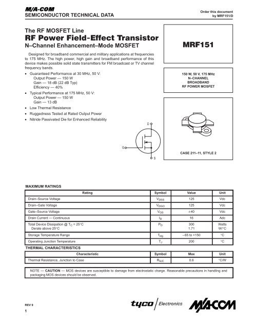
RF Power Field-Effect Transistor MRF151 - CB Tricks
RF Power Field-Effect Transistor MRF151 - CB Tricks
RF Power Field-Effect Transistor MRF151 - CB Tricks

You also want an ePaper? Increase the reach of your titles
YUMPU automatically turns print PDFs into web optimized ePapers that Google loves.
<strong>RF</strong> POWER MOSFET CONSIDERATIONSMOSFET CAPACITANCESThe physical structure of a MOSFET results in capacitorsbetween the terminals. The metal anode gate structure determinesthe capacitors from gate–to–drain (C gd ), and gate–to–source (C gs ). The PN junction formed during thefabrication of the MOSFET results in a junction capacitancefrom drain–to–source (C ds ).These capacitances are characterized as input (C iss ), output(C oss ) and reverse transfer (C rss ) capacitances on datasheets. The relationships between the inter–terminal capacitancesand those given on data sheets are shown below. TheC iss can be specified in two ways:1. Drain shorted to source and positive voltage at the gate.2. Positive voltage of the drain in respect to source and zerovolts at the gate. In the latter case the numbers are lower.However, neither method represents the actual operatingconditions in <strong>RF</strong> applications.GATEC gdC gsDRAINC dsSOURCEC iss = C gd = C gsC oss = C gd = C dsC rss = C gdLINEARITY AND GAIN CHARACTERISTICSIn addition to the typical IMD and power gain data presented,Figure 6 may give the designer additional informationon the capabilities of this device. The graph represents thesmall signal unity current gain frequency at a given drain currentlevel. This is equivalent to f T for bipolar transistors.Since this test is performed at a fast sweep speed, heating ofthe device does not occur. Thus, in normal use, the highertemperatures may degrade these characteristics to some extent.DRAIN CHARACTERISTICSOne figure of merit for a FET is its static resistance in thefull–on condition. This on–resistance, V DS(on) , occurs in thelinear region of the output characteristic and is specified underspecific test conditions for gate–source voltage and draincurrent. For MOSFETs, V DS(on) has a positive temperaturecoefficient and constitutes an important design considerationat high temperatures, because it contributes to the powerdissipation within the device.GATE CHARACTERISTICSThe gate of the MOSFET is a polysilicon material, and iselectrically isolated from the source by a layer of oxide. Theinput resistance is very high — on the order of 10 9 ohms —resulting in a leakage current of a few nanoamperes.Gate control is achieved by applying a positive voltageslightly in excess of the gate–to–source threshold voltage,V GS(th) .Gate Voltage Rating — Never exceed the gate voltagerating. Exceeding the rated V GS can result in permanentdamage to the oxide layer in the gate region.Gate Termination — The gate of this device is essentiallycapacitor. Circuits that leave the gate open–circuited or floatingshould be avoided. These conditions can result in turn–on of the device due to voltage build–up on the inputcapacitor due to leakage currents or pickup.Gate Protection — This device does not have an internalmonolithic zener diode from gate–to–source. If gate protectionis required, an external zener diode is recommended.Using a resistor to keep the gate–to–source impedancelow also helps damp transients and serves another importantfunction. Voltage transients on the drain can be coupled tothe gate through the parasitic gate–drain capacitance. If thegate–to–source impedance and the rate of voltage changeon the drain are both high, then the signal coupled to the gatemay be large enough to exceed the gate–threshold voltageand turn the device on.HANDLING CONSIDERATIONSWhen shipping, the devices should be transported only inantistatic bags or conductive foam. Upon removal from thepackaging, careful handling procedures should be adheredto. Those handling the devices should wear grounding strapsand devices not in the antistatic packaging should be kept inmetal tote bins. MOSFETs should be handled by the caseand not by the leads, and when testing the device, all leadsshould make good electrical contact before voltage is applied.As a final note, when placing the FET into the system itis designed for, soldering should be done with a groundediron.DESIGN CONSIDERATIONSThe M<strong>RF</strong>151 is an <strong>RF</strong> <strong>Power</strong>, MOS, N–channel enhancementmode field–effect transistor (FET) designed for HF andVHF power amplifier applications.M/A-COM Application Note AN211A, FETs in Theory andPractice, is suggested reading for those not familiar with theconstruction and characteristics of FETs.The major advantages of <strong>RF</strong> power MOSFETs includehigh gain, low noise, simple bias systems, relative immunityfrom thermal runaway, and the ability to withstand severelymismatched loads without suffering damage. <strong>Power</strong> outputcan be varied over a wide range with a low power dc controlsignal.DC BIASThe M<strong>RF</strong>151 is an enhancement mode FET and, therefore,does not conduct when drain voltage is applied. Draincurrent flows when a positive voltage is applied to the gate.<strong>RF</strong> power FETs require forward bias for optimum performance.The value of quiescent drain current (I DQ ) is not criticalfor many applications. The M<strong>RF</strong>151 was characterized atI DQ = 250 mA, each side, which is the suggested minimumvalue of I DQ . For special applications such as linear amplification,I DQ may have to be selected to optimize the criticalparameters.The gate is a dc open circuit and draws no current. Therefore,the gate bias circuit may be just a simple resistive dividernetwork. Some applications may require a more elaboratebias system.GAIN CONTROL<strong>Power</strong> output of the M<strong>RF</strong>151 may be controlled from itsrated value down to zero (negative gain) by varying the dcgate voltage. This feature facilitates the design of manualgain control, AGC/ALC and modulation systems.REV 97
PACKAGE DIMENSIONSAUMNOTES:1. DIMENSIONING AND TOLERANCING PER ANSIY14.5M, 1982.2. CONTROLLING DIMENSION: INCH.JQ12K34DMRBINCHES MILLIMETERSDIM MIN MAX MIN MAXA 0.960 0.990 24.39 25.14B 0.465 0.510 11.82 12.95C 0.229 0.275 5.82 6.98D 0.216 0.235 5.49 5.96E 0.084 0.110 2.14 2.79H 0.144 0.178 3.66 4.52J 0.003 0.007 0.08 0.17K 0.435 ––– 11.05 –––M 45 NOM 45 NOMQ 0.115 0.130 2.93 3.30R 0.246 0.255 6.25 6.47U 0.720 0.730 18.29 18.54HECSEATINGPLANESTYLE 2:PIN 1. SOURCE2. GATE3. SOURCE4. DRAINCASE 211–11ISSUE NSpecifications subject to change without notice.• North America: Tel. (800) 366-2266, Fax (800) 618-8883• Asia/Pacific: Tel.+81-44-844-8296, Fax +81-44-844-8298• Europe: Tel. +44 (1344) 869 595, Fax+44 (1344) 300 020Visit www.macom.com for additional data sheets and product information.REV 98