Design of a Novel Economic Multiplier in VLSI using Reversible ...
Design of a Novel Economic Multiplier in VLSI using Reversible ...
Design of a Novel Economic Multiplier in VLSI using Reversible ...

Create successful ePaper yourself
Turn your PDF publications into a flip-book with our unique Google optimized e-Paper software.
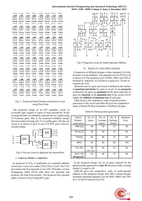
International Journal <strong>of</strong> Eng<strong>in</strong>eer<strong>in</strong>g and Advanced Technology (IJEAT)ISSN: 2249 – 8958, Volume-2, Issue-2, December 2012Fig 9: Proposed circuit for Multi-Operand AdditionFig. 7: Proposed Partial Product Generation Circuitus<strong>in</strong>g Peres GateThe proposed design <strong>of</strong> an 8*8 multiplier circuit <strong>in</strong>reversible logic requires 8 copies <strong>of</strong> each operand bit. In theexist<strong>in</strong>g literature on multiplier operand bits are copied us<strong>in</strong>g24 Feynman gates. But <strong>in</strong> the proposed multiplier designfan-out is achieved us<strong>in</strong>g only 12 reversible gates. The fan-outcircuit is as shown <strong>in</strong> fig.8. It uses 4*4 BVF gates with twoconstant <strong>in</strong>puts.IV. RESULTS AND DISCUSSIONSComparison <strong>of</strong> different designs is done separately for boththe parts <strong>of</strong> each multiplier. The quantum cost <strong>of</strong> a PFAG [14]is shown as 8.The quantum costs <strong>of</strong> HNG, MKG and TSG isdeclared as „unknown‟ <strong>in</strong> [14] but it is equal to 6, 10 and 10respectively [16].Quantum cost <strong>of</strong> a gate and circuit is def<strong>in</strong>ed as the number<strong>of</strong> quantum operations <strong>in</strong> a gate or circuit. In our proposedarchitecture the gates are quantum but the <strong>in</strong>terconnection <strong>of</strong>gates are classical, so the quantum cost <strong>of</strong> the circuit will besimply the addition <strong>of</strong> quantum cost <strong>of</strong> each gate.Table-II gives the comparative study <strong>of</strong> partial productgeneration <strong>of</strong> the circuit and table-III gives the comparativestudy <strong>of</strong> Partial Product Generation <strong>of</strong> different designs.PartialProductGenerationTable-II: Partial product generationNo. <strong>of</strong>GatesNo. <strong>of</strong>ConstantInputsNo. <strong>of</strong>GarbageOutputQuantumCostMKG[4] 40 40 32 88PFAG[5] 40 40 32 88TSG[6] 40 40 32 88HNG 40 46 80 104Fig 8: Fan-out circuit to duplicate the operand bits2. PARTIAL PRODUCT ADDITION:As proposed <strong>in</strong> [12], to implement an n-operand additioncircuit part a carry save adder [18] (CSA) is used. The CSAtree reduces the four operands to two [19]. Thereafter, a CarryPropagat<strong>in</strong>g Adder (CPA) adds these two operands andproduces the f<strong>in</strong>al 8-bit product. The proposed four operandadder is shown <strong>in</strong> Fig 9 us<strong>in</strong>g BVF gate.FG+PG 40 40 32 84(24+16)BVF+PG(Proposed)28 40 32 88In the proposed design, the no <strong>of</strong> gates required for thepartial product generation is only 28 whereas <strong>in</strong> other exist<strong>in</strong>gdesign it is equal to 40.Table-III gives the comparative study <strong>of</strong> multi-operandaddition <strong>of</strong> the proposed design with other exist<strong>in</strong>g designsassum<strong>in</strong>g m<strong>in</strong>imum quantum cost for HNG, MKG and TSGas 6, 10 and 10 respectively [16].319