Design of a Novel Economic Multiplier in VLSI using Reversible ...
Design of a Novel Economic Multiplier in VLSI using Reversible ...
Design of a Novel Economic Multiplier in VLSI using Reversible ...
You also want an ePaper? Increase the reach of your titles
YUMPU automatically turns print PDFs into web optimized ePapers that Google loves.
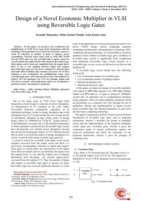
International Journal <strong>of</strong> Eng<strong>in</strong>eer<strong>in</strong>g and Advanced Technology (IJEAT)ISSN: 2249 – 8958, Volume-2, Issue-2, December 2012<strong>Design</strong> <strong>of</strong> a <strong>Novel</strong> <strong>Economic</strong> <strong>Multiplier</strong> <strong>in</strong> <strong>VLSI</strong>us<strong>in</strong>g <strong>Reversible</strong> Logic GatesKoushik Majumder, Malay Kumar Pandit, Asim Kumar JanaAbstract— In this paper, we present a new architecture formultiplication <strong>in</strong> <strong>VLSI</strong> (Very Large Scale Integration) with theadvantage <strong>of</strong> less quantum cost as well as less transistor count as aresult <strong>of</strong> reduction <strong>in</strong> number <strong>of</strong> gates to improve powerconsumption. Classical Logic Gates such as AND, OR, NAND(Except NOT) gates are not reversible that is <strong>in</strong>puts cannot berecovered from the output. On the other hand, <strong>in</strong> <strong>Reversible</strong> LogicGates <strong>in</strong>puts can be recovered completely from the output that isthere is one to one mapp<strong>in</strong>g between <strong>in</strong>puts and outputs.<strong>Reversible</strong> logic gates use less power compared to classical gatesand under ideal condition, they consume zero power. So we havedesigned a new architecture for multiplication us<strong>in</strong>g somereversible logic gates - BVF gate and Peres Gate. This helped us toachieve 24% less quantum cost, 15% less garbage output, and23% less no. <strong>of</strong> gates, which effectively reduces no. <strong>of</strong> transistors,and hence power consumption is m<strong>in</strong>imum.Index Terms— Adder, Garbage Output, <strong>Multiplier</strong>, QuantumCost, <strong>Reversible</strong> Logic, <strong>VLSI</strong>.I. INTRODUCTIONOne <strong>of</strong> the major goals <strong>in</strong> <strong>VLSI</strong> (Very Large ScaleIntegration) circuit design is reduction <strong>of</strong> power dissipation.As demonstrated by R. Landauer <strong>in</strong> the early 1960s,irreversible hardware computation, regardless <strong>of</strong> itsrealization technique, results <strong>in</strong> energy dissipation due to the<strong>in</strong>formation loss [1]. It is proved that the loss <strong>of</strong> each one bit<strong>of</strong> <strong>in</strong>formation dissipates at least kTln2 joules <strong>of</strong> energy(heat), where k=1.3806505x10 -23 m 2 kg -2 K -1 (joules Kelv<strong>in</strong> -1 )is the Boltzmann‟s constant and T is the absolute temperatureat which operation is performed [2]. <strong>Reversible</strong> logic circuitshave theoretically zero <strong>in</strong>ternal power dissipation becausethey do not lose <strong>in</strong>formation. Hence, <strong>in</strong> 1973, Bennett showedthat <strong>in</strong> order to avoid kTln2 joules <strong>of</strong> energy dissipation <strong>in</strong> acircuit, it must be built us<strong>in</strong>g reversible logic gates [3].A circuit is said to be reversible if the <strong>in</strong>put vector can beuniquely recovered from the output vector and there is aone-to-one correspondence between its <strong>in</strong>puts and outputs.Such gates or circuits allow the reproduction <strong>of</strong> the <strong>in</strong>putsfrom observed outputs and we can determ<strong>in</strong>e the <strong>in</strong>puts fromthe outputs [4-6], i.e. not only the outputs can be uniquelydeterm<strong>in</strong>ed from the <strong>in</strong>puts, but also the <strong>in</strong>puts can berecovered from the outputs [5-7]. Thus, the number <strong>of</strong> <strong>in</strong>putsand outputs <strong>in</strong> reversible logic gates or circuits are equal.<strong>Reversible</strong> logic has received significant attention <strong>in</strong> recentyears. It has applications <strong>in</strong> various research areas such as lowpower CMOS design, optical comput<strong>in</strong>g, quantumcomput<strong>in</strong>g, bio<strong>in</strong>formatics, thermodynamic technology, DNAcomput<strong>in</strong>g and nanotechnology. It is not possible to constructquantum circuits without reversible logic gates. Synthesis <strong>of</strong>reversible logic circuits is significantly more complicatedthan traditional irreversible logic circuits because <strong>in</strong> areversible logic circuit, we are not allowed to use fan-out andfeedback [5].A reversible logic circuit should have the follow<strong>in</strong>gfeatures [6]:• Use <strong>of</strong> m<strong>in</strong>imum number <strong>of</strong> reversible gates.• Use <strong>of</strong> m<strong>in</strong>imum number <strong>of</strong> garbage outputs.• M<strong>in</strong>imized quantum cost.• M<strong>in</strong>imized transistor countIn this paper, an improved design <strong>of</strong> reversible multiplierwith respect to 24% less quantum cost, 15% less GarbageOutput and 23% less no. <strong>of</strong> gates is proposed. <strong>Multiplier</strong>circuits play an important role <strong>in</strong> computational operationus<strong>in</strong>g computers. There are many arithmetic operations whichare performed, on a computer ALU [8], through the use <strong>of</strong>multipliers. <strong>Design</strong> and implementation <strong>of</strong> digital circuitsus<strong>in</strong>g reversible logic has attracted popularity to ga<strong>in</strong> entry<strong>in</strong>to the future comput<strong>in</strong>g technology.This paper is organized as follows: Section 2 gives the brief<strong>in</strong>troduction <strong>of</strong> reversible logic gates used <strong>in</strong> proposedarchitecture. Section 3 describes the design <strong>of</strong> multipliercircuit and the implementation <strong>of</strong> the proposed multipliercircuit us<strong>in</strong>g new reversible gates. Section 4 gives thecomparative study <strong>of</strong> various architectures aga<strong>in</strong>st ourproposed architecture and shows the advantage <strong>of</strong> ourproposed architecture. Section 5 gives the prospect <strong>of</strong>rema<strong>in</strong><strong>in</strong>g work.A. Feynman Gate:II. REVERSIBLE LOGIC GATESFig.1 shows a 2*2 Feynman gate [9]. The <strong>in</strong>put vector is I(A, B) and the output vector is O (P, Q). The outputs aredef<strong>in</strong>ed by P=A, Q=A B. Quantum cost <strong>of</strong> a Feynman gateis 1 [9].Manuscript received on December, 2012.Koushik Majumder, Electronics & Comm. Engg., Haldia Institute OfTechnology, Haldia, East Midnapore, IndiaPr<strong>of</strong>.(Dr.) Malay K. Pandit, Electronics & Comm. Engg., Haldia InstituteOf Technology, Haldia, East Midnapore, IndiaAsim K. Jana, Electronics & Comm. Engg., Haldia Institute OfTechnology, Haldia, East Midnapore, IndiaFig. 1: Feynman Gate317
International Journal <strong>of</strong> Eng<strong>in</strong>eer<strong>in</strong>g and Advanced Technology (IJEAT)ISSN: 2249 – 8958, Volume-2, Issue-2, December 2012Fig 9: Proposed circuit for Multi-Operand AdditionFig. 7: Proposed Partial Product Generation Circuitus<strong>in</strong>g Peres GateThe proposed design <strong>of</strong> an 8*8 multiplier circuit <strong>in</strong>reversible logic requires 8 copies <strong>of</strong> each operand bit. In theexist<strong>in</strong>g literature on multiplier operand bits are copied us<strong>in</strong>g24 Feynman gates. But <strong>in</strong> the proposed multiplier designfan-out is achieved us<strong>in</strong>g only 12 reversible gates. The fan-outcircuit is as shown <strong>in</strong> fig.8. It uses 4*4 BVF gates with twoconstant <strong>in</strong>puts.IV. RESULTS AND DISCUSSIONSComparison <strong>of</strong> different designs is done separately for boththe parts <strong>of</strong> each multiplier. The quantum cost <strong>of</strong> a PFAG [14]is shown as 8.The quantum costs <strong>of</strong> HNG, MKG and TSG isdeclared as „unknown‟ <strong>in</strong> [14] but it is equal to 6, 10 and 10respectively [16].Quantum cost <strong>of</strong> a gate and circuit is def<strong>in</strong>ed as the number<strong>of</strong> quantum operations <strong>in</strong> a gate or circuit. In our proposedarchitecture the gates are quantum but the <strong>in</strong>terconnection <strong>of</strong>gates are classical, so the quantum cost <strong>of</strong> the circuit will besimply the addition <strong>of</strong> quantum cost <strong>of</strong> each gate.Table-II gives the comparative study <strong>of</strong> partial productgeneration <strong>of</strong> the circuit and table-III gives the comparativestudy <strong>of</strong> Partial Product Generation <strong>of</strong> different designs.PartialProductGenerationTable-II: Partial product generationNo. <strong>of</strong>GatesNo. <strong>of</strong>ConstantInputsNo. <strong>of</strong>GarbageOutputQuantumCostMKG[4] 40 40 32 88PFAG[5] 40 40 32 88TSG[6] 40 40 32 88HNG 40 46 80 104Fig 8: Fan-out circuit to duplicate the operand bits2. PARTIAL PRODUCT ADDITION:As proposed <strong>in</strong> [12], to implement an n-operand additioncircuit part a carry save adder [18] (CSA) is used. The CSAtree reduces the four operands to two [19]. Thereafter, a CarryPropagat<strong>in</strong>g Adder (CPA) adds these two operands andproduces the f<strong>in</strong>al 8-bit product. The proposed four operandadder is shown <strong>in</strong> Fig 9 us<strong>in</strong>g BVF gate.FG+PG 40 40 32 84(24+16)BVF+PG(Proposed)28 40 32 88In the proposed design, the no <strong>of</strong> gates required for thepartial product generation is only 28 whereas <strong>in</strong> other exist<strong>in</strong>gdesign it is equal to 40.Table-III gives the comparative study <strong>of</strong> multi-operandaddition <strong>of</strong> the proposed design with other exist<strong>in</strong>g designsassum<strong>in</strong>g m<strong>in</strong>imum quantum cost for HNG, MKG and TSGas 6, 10 and 10 respectively [16].319
Malay Kumar Pandit received his B.E and M. E degrees<strong>in</strong> Electronics Eng<strong>in</strong>eer<strong>in</strong>g from Electronics and TelecomEngg Dept., Jadavpur University, India <strong>in</strong> 1989 and 1991,respectively. He received his PhD from UK‟s renownedCambridge University <strong>in</strong> 1996. He did his post-doc fromthe Optoelectronics Research Centre, City University <strong>of</strong>Hong Kong till 2002 where he pioneered the use <strong>of</strong> polymers for opticalwaveguide applications. .He then took a corporate career where he worked <strong>in</strong>a fiber optic company ―FONS (I) Ltd‖ <strong>in</strong> the doma<strong>in</strong> <strong>of</strong> optical network<strong>in</strong>g.Now he is a full Pr<strong>of</strong>essor <strong>in</strong> the Electronics Engg Dept. and Dean <strong>of</strong> School<strong>of</strong> Eng<strong>in</strong>eer<strong>in</strong>g <strong>of</strong> the reputed Haldia Institute <strong>of</strong> Technology where hefocuses on embedded systems and grid comput<strong>in</strong>g, <strong>in</strong>clud<strong>in</strong>g their usage <strong>in</strong>WDM optical networks. He currently leads a MODROBS project <strong>of</strong> theAICTE, Govt <strong>of</strong> India on embedded electronic systems. He has 45<strong>in</strong>ternational publications <strong>in</strong> this area. Dr. Pandit was awarded the NationalScholarship <strong>of</strong> the Government <strong>of</strong> India <strong>in</strong> 1983 and the Nehru Scholarship<strong>of</strong> the Government <strong>of</strong> India dur<strong>in</strong>g his Ph.D. studies.Asim Kumar Jana received his bachelor‟s andmaster‟s degree <strong>in</strong> Electronics & Telecomm Engg andMBA, respectively, from Jadavpur University, India<strong>in</strong> 1988 and 1995, respectively. He has 10 years <strong>of</strong><strong>in</strong>dustrial experience <strong>in</strong> the doma<strong>in</strong> <strong>of</strong> embeddedsystems. Currently he is an associate pr<strong>of</strong>essor oncomputer systems. He has 10 <strong>in</strong>ternational researchpapers.International Journal <strong>of</strong> Eng<strong>in</strong>eer<strong>in</strong>g and Advanced Technology (IJEAT)ISSN: 2249 – 8958, Volume-2, Issue-2, December 2012321


