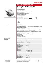
SSI / BiSS - Hengstler GmbH
SSI / BiSS - Hengstler GmbH
SSI / BiSS - Hengstler GmbH

Create successful ePaper yourself
Turn your PDF publications into a flip-book with our unique Google optimized e-Paper software.
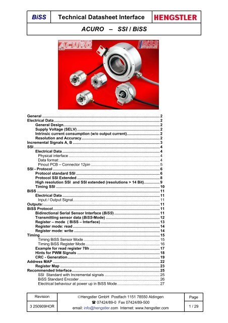
<strong>BiSS</strong>Technical Datasheet InterfaceACURO – <strong>SSI</strong> / <strong>BiSS</strong>General ............................................................................................................... 2Electrical Data.................................................................................................... 2General Design........................................................................................... 2Supply Voltage (SELV) .............................................................................. 2Intrinsic current consumption (w/o output current)............................... 2Resolution and Accuracy.......................................................................... 2Incremental Signals A, B .................................................................................. 3<strong>SSI</strong> ....................................................................................................................... 4Electrical Data ............................................................................................ 4Physical interface ...................................................................................... 4Data format:............................................................................................... 4Pinout PCB – Connector 12pin ................................................................. 5<strong>SSI</strong> - Protocol ..................................................................................................... 6Protocol standard <strong>SSI</strong> ............................................................................... 6Protocol <strong>SSI</strong> Extended .............................................................................. 8High resolution <strong>SSI</strong> and <strong>SSI</strong> extended (resolutions > 14 Bit)............... 9Timing <strong>SSI</strong> .................................................................................................. 10<strong>BiSS</strong> .................................................................................................................... 11Electrical Data ............................................................................................ 11Input / Output Signal.................................................................................. 11Outputs:.............................................................................................................. 11<strong>BiSS</strong> Protocol..................................................................................................... 11Bidirectional Serial Sensor Interface (<strong>BiSS</strong>) ........................................... 11Transmitting sensor data (<strong>BiSS</strong>-Mode) ................................................... 12Register – mode ( <strong>BiSS</strong> – Interface)........................................................ 13Register mode: read .................................................................................. 14Register mode: write ................................................................................. 14Timing ................................................................................................................. 15Timing <strong>BiSS</strong> Sensor Mode ........................................................................ 15Timing <strong>BiSS</strong> Register Mode ...................................................................... 16Example for read register 78h .................................................................. 17Hints for PWM Signals .............................................................................. 18CRC - Generation....................................................................................... 19Address MAP ..................................................................................................... 22Register Map .............................................................................................. 23Recommended Interface................................................................................... 25<strong>SSI</strong> Standard with Incremental signals .................................................... 25<strong>BiSS</strong> Standard Encoder ............................................................................ 26Electrical behaviour at power up in <strong>BiSS</strong> Mode ........................................ 27Revision3 250909HOR©<strong>Hengstler</strong> <strong>GmbH</strong> Postfach 1151 78550 Aldingen 07424/89-0 Fax 07424/89-500email: info@hengstler.com Internet: www.hengstler.comPage1 / 29
<strong>BiSS</strong>Technical Datasheet InterfaceACURO – <strong>SSI</strong> / <strong>BiSS</strong>CableFor clock and data should be twisted in pairs and shieldedBaud rate / Cable lengthcable length Baud rate< 25 m < 1 MHz< 50 m < 400 kHz< 100 m < 300 kHz< 200 m < 200 kHz< 400 m < 100 kHzPinout PCB – Connector 12pinRow b5 or 7-30 V Clock B- 0V (UN) A- Data(UB) gr/pk wt rd wt/gn ye bkRow aData/ A+ 0V Sens B+ Clock/ 5 V Sensvio gn bn/gn bl bn rd/blPIN 1 2 3 4 5 6Hint:5 V (UB) 5 V Sens0 V (UN) 0 V SensConnection on encoder side over12-pin PCB connector,Manufacturer Berg, Type: Minitek.Revision3 250909HOR©<strong>Hengstler</strong> <strong>GmbH</strong> Postfach 1151 78550 Aldingen 07424/89-0 Fax 07424/89-500email: info@hengstler.com Internet: www.hengstler.comPage5 / 29
<strong>BiSS</strong>Technical Datasheet InterfaceACURO – <strong>SSI</strong> / <strong>BiSS</strong><strong>SSI</strong> - ProtocolProtocol standard <strong>SSI</strong>The <strong>SSI</strong> data transmission of an absolute encoder position value is based on a shift register, wherethe shift clock is provided by the external control. The encoder provides its position data anddepending on configuration also status information synchronous to the external clock on the data line.Both lines are physically according to RS422 specification.Clock pulse diagramTransmission CycleFor correct transfer of the data a defined number of impulses (clock pulse brush) must be applied tothe clock input of the absolute shaft encoder. Next, a pause TP must be observed.As soon as a clock pulse brush is applied to the clock pulse input, the actual angle information will belatched.With the first shift of the clock signal from low to high the most significant bit (MSB) of the angulardata is applied to the shaft encoder’s serial output. With each succeeding rising edge, the next lesssignificant bit is shifted to the data output. After transmission of the least significant bit (LSB) the Alarmbit or other special bits are transferred, depending on configuration. Then the data line switches to low until the time tm has passed. A further transfer of data cannot be started until the data line switchesto high again. If the clock pulse sequence is not interrupted at point , the ring-register mode isactivated automatically. This means that the data stored at the first clock pulse transition arereturned to the serial input Si via the terminal SO. As long as the clock pulse is not interrupted at ,the data can be read out as often as wanted (multiple transfer). The number of clock pulses necessaryfor data transfer is independent of the resolution of the absolute shaft encoder. The clock signal canbe interrupted at any point, or continued in ring-register mode for repeated polling.Revision3 250909HOR©<strong>Hengstler</strong> <strong>GmbH</strong> Postfach 1151 78550 Aldingen 07424/89-0 Fax 07424/89-500email: info@hengstler.com Internet: www.hengstler.comPage6 / 29
<strong>BiSS</strong>Technical Datasheet InterfaceACURO – <strong>SSI</strong> / <strong>BiSS</strong>With a data length of 25 Bit (simple transmission) the transmission after the lowest Bit (LSB), the dataline holds on low, till the time tm is elapsed.Clock frequency: 100 kHz.....1,5 MHzMonoflop time tm : 12 µs =tm =20 µsClock pulse brush : 25 Clock cycles for Multiturn13 Clock cycles for SingelturnRevision3 250909HOR©<strong>Hengstler</strong> <strong>GmbH</strong> Postfach 1151 78550 Aldingen 07424/89-0 Fax 07424/89-500email: info@hengstler.com Internet: www.hengstler.comPage7 / 29
<strong>BiSS</strong>Technical Datasheet InterfaceACURO – <strong>SSI</strong> / <strong>BiSS</strong>Protocol <strong>SSI</strong> Extended<strong>SSI</strong> interface: extended <strong>SSI</strong> formatsIn extended <strong>SSI</strong> mode singleturn data of up to 21 bits and an additional 12 to 24 bits of multiturn datacan be transmitted. This is followed by the 8-bit temperature value.Expansions compared to <strong>SSI</strong> standard format:After the position data there are two additional bits that indicate the status of the encoder. First thealarm bit and then the warning bit.The reports from the LED current control or the temperature control can be assigned freely betweenthe two bits (alarm, warning).In the standard version the alarm bit is assigned to the LED current control and the warning bit isassigned to the internal temperature sensor.Function: If one of the fault conditions occurs, the alarm bit is set “high” (‚1’bit in the protocol). Afterreading a new position value the alarm bit is cleared automatically again. If the cause for the alarm isnot longer present, the alarm bit is set to ‘0’ (in the protocol is like '0'). Should the cause still bepresent, the alarm bit is set once more ('1').6 Bit CRC ChecksumTo guarantee a safe data transmission, there is a 6 bit CRC checksum over data and status bits.The start value of the checksum is 43h (1000011b) . The checksum is formed and transferred ininverted format. First of the 6 Bit CRC transmitted is CRC5 CRC0.TemperatureA temperature sensor with a resolution of 1 °C (LSB) within a range of -64 °C to +191 °C has beenincluded on the internal OptoAsic chip for the monitoring of the operating temperature. The currenttemperature is stored as an 8-bit value. The sensor is calibrated in such a way that the value "01000000" is produced at 0 °C. The sensor sets error bit when either the upper or lower alarm thresholdshave been exceeded.Example temperature value = 59h (59h –40h = 19h) temperature 25° C4 Bit CRC ChecksumTo guarantee a safe temperature transmission, there is a 4 bit CRC checksumThe start value of the checksum is 13h (10011b) . The checksum is formed and transferred invertedformat. First of the 4 Bit CRC transmitted is CRC3 CRC0.Revision3 250909HOR©<strong>Hengstler</strong> <strong>GmbH</strong> Postfach 1151 78550 Aldingen 07424/89-0 Fax 07424/89-500email: info@hengstler.com Internet: www.hengstler.comPage8 / 29
<strong>BiSS</strong>Technical Datasheet InterfaceACURO – <strong>SSI</strong> / <strong>BiSS</strong>High resolution <strong>SSI</strong> and <strong>SSI</strong> extended (resolutions > 14 Bit)For Singleturn resolutions > 14 Bit either the Clock frequency must not exceed 100 kHz, or with higherclock frequencies the first negative Clock pulse needs to be on low level for minimun t SAR time.This is due to the time needed for internal A/D conversion.TransmitDataClockt SART m =10...30µsDataMSBLSB*need only for Singleturn resolutions > 14 BitExample how to calculate t SAR : The resolution of the encoder shall be 1217, so the single turn part is17 bit. The 17 bit consists internally of 11 bit digital information and 6 bit interpolated information. Sowe need time for 6 bits interpolation. If n is the number of interpolation bits we need (worst case) 600 *(n+1) ns calculation time. Now you can calculate the delay: it is (6bit + 1) * 600ns= 4,2 µs . After thistime the output value is ready to be transmitted.Revision3 250909HOR©<strong>Hengstler</strong> <strong>GmbH</strong> Postfach 1151 78550 Aldingen 07424/89-0 Fax 07424/89-500email: info@hengstler.com Internet: www.hengstler.comPage9 / 29
<strong>BiSS</strong>Technical Datasheet InterfaceACURO – <strong>SSI</strong> / <strong>BiSS</strong>Timing <strong>SSI</strong>TMASClockt reqT MASlT MAShtimeoutDataMSBLSB*needed only for Singleturn resolutions > 14 Bit<strong>SSI</strong> ModeSymbol Parameter Conditions min typ max. Unittimeout sens (Ttos)* 9,9 12,4 14,9 µsTMAS Permissible Clock Period 250 ns 2*TtostMAShClock Signal Hi Level125 Ttos nsDurationtMASlClock Signal Lo Level125 Ttos nsDurationtreqData Request Lo Level only with SAR t SAR Ttos nsDurationconverterfclk Clock Frequency 4 5 6 MHztSARConversion Time SARConvertern = resolution ofSAR converter2(n+1)/fclk µS* Ttos = is programmable TimeRevision3 250909HOR©<strong>Hengstler</strong> <strong>GmbH</strong> Postfach 1151 78550 Aldingen 07424/89-0 Fax 07424/89-500email: info@hengstler.com Internet: www.hengstler.comPage10 / 29
<strong>BiSS</strong>Technical Datasheet InterfaceACURO – <strong>SSI</strong> / <strong>BiSS</strong><strong>BiSS</strong>Electrical DataInput / Output SignalClock and /Clock:RS485 (Input)Data and /Data:RS485 (Output)Clock frequency :100 kHz.....10 MHzTimeout SENS *: 12µsTimout reg .*: 51µs* Timeout SENS and timeout reg are programmableOutputs:Driver output current :Short circuit output current :max.60 mA± 250 mACableLeads for clock and data should be twisted in pairsEntire cable shielded and according to CAT 5Cable capacity ≤ 100 pF/mCable length max 100 mBaud rate < 10 MHz<strong>BiSS</strong> ProtocolBidirectional Serial Sensor Interface (<strong>BiSS</strong>)The Serial <strong>BiSS</strong> communication differentiates between the fast transmission of sensor data and theslower transmission of register data. The transmission of sensor data is unidirectional; here, ACUROcan only output data, whereas the bidirectional transmission of register data can include read andwrite access.The <strong>BiSS</strong> sensor interface can be operated in an <strong>SSI</strong> compatible mode, in which only a lowertransmission speed is possible and ACURO may not demand processing time for procedures such asinterpolation, for example.Revision3 250909HOR©<strong>Hengstler</strong> <strong>GmbH</strong> Postfach 1151 78550 Aldingen 07424/89-0 Fax 07424/89-500email: info@hengstler.com Internet: www.hengstler.comPage11 / 29
<strong>BiSS</strong>Technical Datasheet InterfaceACURO – <strong>SSI</strong> / <strong>BiSS</strong>Transmitting sensor data (<strong>BiSS</strong>-Mode)Transmission is initiated by a falling edge on the master line (MA). The master then again ramps themaster line up to high within a stipulated period (
<strong>BiSS</strong>Technical Datasheet InterfaceACURO – <strong>SSI</strong> / <strong>BiSS</strong>Register – mode ( <strong>BiSS</strong> – Interface)The register communication is initiated by a low signal following the first falling edge from the masteron the clock line. The master keeps the clock line on low until the ACURO reacts with a falling edge onthe data line and thus signaled the change over to register mode. After this has happened the mastertransmits the addressing data coded as a PWM signal (pulse width modulated clock signal). Theindividual sensors (slaves) are addressed by slave IDs which are generated automatically according tothe order of the slaves in the sequential circuit. ACURO uses two slave Ids (e.g. ID "000" and "001")so that it can extend the available addressing range from 7 to 8 bits.Revision3 250909HOR©<strong>Hengstler</strong> <strong>GmbH</strong> Postfach 1151 78550 Aldingen 07424/89-0 Fax 07424/89-500email: info@hengstler.com Internet: www.hengstler.comPage13 / 29
<strong>BiSS</strong>Technical Datasheet InterfaceACURO – <strong>SSI</strong> / <strong>BiSS</strong>Register mode: readOnce ACURO has signaled the changeover to register mode the master transmits the start bit, the 3-bit slave ID and the 7-bit register address for the addressing sequence, followed by the WNR bit ("0")and the 6-bit CRC. Each bit is coded by the duty cycle (PWM), including the start bit. The generatorpolynomial for the 4-bit CRC is 0x13 = "10011" (see the definitions in the description of the <strong>BiSS</strong>protocol). The ACURO does not require any processing time to read the internal registers andanswers immediately with the data of the addressed registers. When reading the external EEPROMregisters the output is delayed until the data from the EEPROM has been made available. All 8-bitread data can also be checked for transmission errors by the 4-bit CRC 0x13.3 *ID, 7 * ADR, WNR, 6 * CRCStartStopMAStopSLStartData7Data0/CRC3/CRC0StopLock< timeoutSENS timeoutSRegister mode: writeWhen data is being written to a register, after the ACURO has confirmed the mode changeover thesame addressing sequence as for read access is used (with the WNR bit at "1"). Following the secondstart bit the master transmits the data to be written which ACURO returns for verification, bit by bit oneclock pulse later. As in the above, a 4-bit CRC have to follow the 8-bit write data which is returned byACURO in the same manner, however not in PWM format. A transfer to the EEPROM registers isprocessed in the background and can be validated by a read access once transmission is over.Address : 3 *ID, 7 * ADR,StartData7Data0StopMAStopSLStartData7Data0/CRC3/CRC0StopLock< timeout SENS timeoutSENSRevision3 250909HOR©<strong>Hengstler</strong> <strong>GmbH</strong> Postfach 1151 78550 Aldingen 07424/89-0 Fax 07424/89-500email: info@hengstler.com Internet: www.hengstler.comPage14 / 29
<strong>BiSS</strong>Technical Datasheet InterfaceACURO – <strong>SSI</strong> / <strong>BiSS</strong>TimingTiming <strong>BiSS</strong> Sensor ModeClock Clock Clock Clock Clock nTMAMAReqSLtreqACKStart Data Data StopT MAShT MASltimeout sens<strong>BiSS</strong> Sensor ModeSymbol Parameter Conditions min typ max. Unittimeout sens (Ttos)* 9,9 12,4 14,9 µsTMAS Permissible Clock Period 100 ns 2* TtostMAShtMASlTreqClock Signal Hi LevelDurationClock Signal Lo LevelDurationData Request Lo LevelDurationonly with SARconverter50 Ttos ns50 Ttos ns50 Ttos ns* Ttos = is programmable TimeRevision3 250909HOR©<strong>Hengstler</strong> <strong>GmbH</strong> Postfach 1151 78550 Aldingen 07424/89-0 Fax 07424/89-500email: info@hengstler.com Internet: www.hengstler.comPage15 / 29
<strong>BiSS</strong>Technical Datasheet InterfaceACURO – <strong>SSI</strong> / <strong>BiSS</strong>Timing <strong>BiSS</strong> Register ModeClockClockClockTMATMATMAtMAtMAStopMAStartSLLockDataDataDataDataStopTtosTidlesend ‚0’ send ‚1’clock outTtor<strong>BiSS</strong> Register ModeSymbol Parameter Conditions Min Max. UnitTMAR Permissible Clock Period CFGTOR = 2Eh 4 52 µstidle Permissible Clock Halt (idle) 0 IndefinitetMARhClock Signal Hi Level read out of register 50 % % TMARDurationdatatMARlClock Signal Lo LevelTtor nsDurationtMA0h .Logic 0" Hi Level Duration 10 30 % TMARtMA1h .Logic 1" Hi Level Duration 70 90 % TMARRevision3 250909HOR©<strong>Hengstler</strong> <strong>GmbH</strong> Postfach 1151 78550 Aldingen 07424/89-0 Fax 07424/89-500email: info@hengstler.com Internet: www.hengstler.comPage16 / 29
<strong>BiSS</strong>Technical Datasheet InterfaceACURO – <strong>SSI</strong> / <strong>BiSS</strong>Example for read register 78hKeep clock active until start bit is sent by encoder. Approx. time ~ 416 µs416µsSee Figure: The clock should be applied until encoder sends ACK ( ~ 416 µs). This time is neededbecause the ASIC has to read the EEPROM internally before sending the data. There are differenttimes for different registers because registers are mapped either directly in the ASIC or externally toan EEPROM value (takes more time).Revision3 250909HOR©<strong>Hengstler</strong> <strong>GmbH</strong> Postfach 1151 78550 Aldingen 07424/89-0 Fax 07424/89-500email: info@hengstler.com Internet: www.hengstler.comPage17 / 29
<strong>BiSS</strong>Technical Datasheet InterfaceACURO – <strong>SSI</strong> / <strong>BiSS</strong>Hints for PWM SignalsCode sample for PWM with port bitClock ClockTMA TMAtransmit ‚0’trans_0 :; 1 time high 3 time lowset portx; Output = highclear portx ; Output lowclear portx ; Output lowclear portx ; Output lowret ; end send ‘0’trans_1 :; 3 time high 1 time lowset portx; Output = highset portx; Output = highset portx; Output = highclear portx ; Output = lowret ; end send ‘1’x = Output Pin MACode sample for PWM with SPI1 0 0 0 1 1 1 0transmit ‚0’transmit ‚1’Revision3 250909HOR©<strong>Hengstler</strong> <strong>GmbH</strong> Postfach 1151 78550 Aldingen 07424/89-0 Fax 07424/89-500email: info@hengstler.com Internet: www.hengstler.comPage18 / 29
<strong>BiSS</strong>Technical Datasheet InterfaceACURO – <strong>SSI</strong> / <strong>BiSS</strong>CRC - GenerationDepending on the configuration the length of the position data varies between 9 and 45 bits, plus anerror bit and a warning bit. With a maximum length of 47 bits this data is protected by a 6-bit cyclicredundancy check value or CRC (polynomial 0x43 = "1000011") which directly follows the data.A CRC "checksum" is the remainder of a binary division with no bit carry ( XOR used instead ofsubtraction), of the message bit stream, by a predefined (short) bit stream of length n, which representthe coefficients of a polynomial. Before the division, n zeros are appended to the message stream.Example:The Bit stream 1000011 is equivalent to the Polynom 1x 6 + 0x 5 + 0x 4 + 0x 3 + 0x 2 + 1x 1 + 1x 0= x 6 + x 1 + 1HardwareDataMSBDataCRCSETProcess:1 Shift register set to 02. Shift Data3. Shift CRC1 = Data0 = CRCRevision3 250909HOR©<strong>Hengstler</strong> <strong>GmbH</strong> Postfach 1151 78550 Aldingen 07424/89-0 Fax 07424/89-500email: info@hengstler.com Internet: www.hengstler.comPage19 / 29
<strong>BiSS</strong>Technical Datasheet InterfaceACURO – <strong>SSI</strong> / <strong>BiSS</strong>//***** function for calculating a new CRC *****//extern byte bitString[bitZ];int calcCRCnew (byte bitPolynom)// contains the data, one data bit per byte// parameter = 4 or 6 bit CRC{// CRC calculating for 4 bit polynom 1 0011 and 6 bit polynom 110 0011// XOR - function only by MSB = high of the working bytes !// Variablebyte crcByte, polynom ; // resulting crc byteint tmpx, msb, zB, tmpy; // temporary variablesif(bitPolynom==4) {zB=4;polynom = 0x13;}else if(bitPolynom == 6){zB=6;polynom = 0x63;}crcByte = 0;// calculate 4 Bit CRC or 6 Bit CRC// start value// BitString mit 4 oder 6 Nullen füllen// clear BitString for 4 or 6 bitsfor (tmpx = bitZ; bitZ < tmpx +bitPolynom;bitZ++) {bitString[bitZ] = 0;}// first fill up crc byte up to polynom lengthfor (tmpx=0,tmpy = bitPolynom;tmpx bitPolynom) & 1 ) { // check if MSB is 1crcByte = ( crcByte ^ polynom );// then do the exor}// shift++ zB;if (zB == bitZ) // check if all bits shifted ?break;// finishedelse {crcByte = (crcByte
<strong>BiSS</strong>Technical Datasheet InterfaceACURO – <strong>SSI</strong> / <strong>BiSS</strong>Sample: Set Preset4 Stop StartRevision3 250909HOR©<strong>Hengstler</strong> <strong>GmbH</strong> Postfach 1151 78550 Aldingen 07424/89-0 Fax 07424/89-500email: info@hengstler.com Internet: www.hengstler.comPage21 / 29
<strong>BiSS</strong>Technical Datasheet InterfaceACURO – <strong>SSI</strong> / <strong>BiSS</strong>Address MAPAddress0x00AccessProtectionBank 0 Bank 1 Bank 2 … 7securityConfigurationData0x5F0x60Command (wr) &Status (rd)RegisterOEMOEM0x610x690x6A0x770x780x7F0x80Position andStatus Data<strong>BiSS</strong> –Device IDOEM128Byte128Byte0xFE0xFFBank selectBank selectBank selectBank 0: 128 Byte - OEM useable MemoryBank 1: 256 Byte - OEM useable MemoryBank 2…7: optionalRevision3 250909HOR©<strong>Hengstler</strong> <strong>GmbH</strong> Postfach 1151 78550 Aldingen 07424/89-0 Fax 07424/89-500email: info@hengstler.com Internet: www.hengstler.comPage22 / 29
<strong>BiSS</strong>Technical Datasheet InterfaceACURO – <strong>SSI</strong> / <strong>BiSS</strong>Register Map0x60Command registerPreset functionWhen the command "Implement PRESET" (data0x02) is written to the command register (address0x60), the current position is written to the external configuration EEPROM as an OFFSET value. Atthe same time the relevant values are written to the six OFFSET registers, one after another.Sequence activity is signaled for a few microseconds after the start of the sequence with a "1" inPRES in the status register (address 0x60, bit 7). The bit switches back to "0" while the sequence isstill running.The entire preset sequence ends after the sixth BUSY "1>0" change (address 0x60, bit 2: serialcommunication active).0x67Temperature Data Register (read only)Bit 7...0 absolute temperature as 8 bit data0x68Error registerBit 7 = Temperature out of defined range default temperature range (see chapter 4.3)Bit 6 = External failure over NERRnot necessary in <strong>BiSS</strong> modeBit 5 = Serial interface failurenot necessary in <strong>BiSS</strong> modeBit 4 = Position data not validnot necessary in <strong>BiSS</strong> modeBit 3 = Failure configuration interface not necessary in <strong>BiSS</strong> modeBit 2 = Position Code ErrorControls the binary code single step by stepBit 1 = External Multiturn ErrorControls the communication between the gear PCBand singleturn PCBBit 0 = LED current out of control range Pollution; Condensation, Over temperature, Ageing ofLED0x78 ..0x7F<strong>BiSS</strong> Device ID0x78 0x41 A Product ID e.g. AC or AD0x79 0x43 C0x7A 0x3A 58 for ACURO0x7B ................................................................................................................................................................................................................................................. resolution0x7Ctimeout0x7D ................................................................................................................................................................................................................................................. free0x7E 0x48 H manufacturer code0x7F 0x45 E <strong>Hengstler</strong>Revision3 250909HOR©<strong>Hengstler</strong> <strong>GmbH</strong> Postfach 1151 78550 Aldingen 07424/89-0 Fax 07424/89-500email: info@hengstler.com Internet: www.hengstler.comPage23 / 29
<strong>BiSS</strong>Technical Datasheet InterfaceACURO – <strong>SSI</strong> / <strong>BiSS</strong>Encoder Characteristics (Produce datas, Resolutions)Reg. Adr. Discription Length Format 1. 2. 3. 4.Reg. 0x34 Serial No. 4 Byte Ser. – No. BCD format SS SS SS LLReg. 0x38 Production- Date 4 Byte Date BCD format DD MM JJ JJReg. 0x3C Article No. 4 Byte Article No. BCD format XX XX XX 0Reg. 0x40 MT- Resolution 1 Byte MT BCD format (0 / 12-Bit) 12Reg. 0x41 ST-Resolution 1 Byte ST BCD format (9...22-Bit) 19Reg. 0x42 Alignment Bits 1 Byte BCD format (0...11-Bit) 5Reg. 0x43 SinCos-Periods 2 Byte SinCos BCD format 20 48Example Data Output <strong>BiSS</strong> ProtocolResolution AD36 1219Reg. 0x40 MT-Resolution 1 Byte MT BCD 12Reg. 0x41 ST- Resolution 1 Byte ST BCD 19Reg. 0x42 Alignment Bits 1 Byte BCD 5MSBMT 12 Bit ST 19 Bit Al 5 Bit CRC BitsResolution AD36 001912 Clocks 24 ClocksReg. 0x40 MT- Resolution 1 Byte MT BCD 0Reg. 0x41 ST- Resolution 1 Byte ST BCD 19Reg. 0x42 Alignment Bits 1 Byte BCD 5MSBST 19 Bit Al 5 Bit CRC BitsResolution AD36 121424 ClocksReg. 0x40 MT- Resolution 1 Byte MT BCD 12Reg. 0x41 ST- Resolution 1 Byte ST BCD 14Reg. 0x42 Alignment Bits 1 Byte BCD 0MSBMT 12 Bit ST 14 Bit CRC Bits12 Clocks 14 ClocksRevision3 250909HOR©<strong>Hengstler</strong> <strong>GmbH</strong> Postfach 1151 78550 Aldingen 07424/89-0 Fax 07424/89-500email: info@hengstler.com Internet: www.hengstler.comPage24 / 29
<strong>BiSS</strong>Technical Datasheet InterfaceACURO – <strong>SSI</strong> / <strong>BiSS</strong>Recommended Interface<strong>SSI</strong> Standard with Incremental signalsz.B. Line-DriverType: ½ 75 179* 1z.B. Line-DriverType ½ 75 179z.B. Optok.PC 410* 1U 1Dimensioning:R1 = 91 Ω , R2 = 100 Ω , R3 = 10 Ω , R4 = 10kΩ ,R5 = R4* desired adjustment, Z0 = 120 ΩC1 = 1nFU1 = 2,5 V ± 0,5V (referred to operating voltage)*1) Alternative population for high transmission rates (> 2MHz) and simultaneousoperation of several encoders (i.e. common clock, separate data lines).Revision3 250909HOR©<strong>Hengstler</strong> <strong>GmbH</strong> Postfach 1151 78550 Aldingen 07424/89-0 Fax 07424/89-500email: info@hengstler.com Internet: www.hengstler.comPage25 / 29
<strong>BiSS</strong>Technical Datasheet InterfaceACURO – <strong>SSI</strong> / <strong>BiSS</strong><strong>BiSS</strong> Standard EncoderSupply10…30 Voltz.B. Line-DriverType: ½ 75 179120 Ohm10 Ohmz.B. Line-DriverType ½ 75 17910 OhmDC5 Volt 10 .. 30 VoltDCRevision3 250909HOR©<strong>Hengstler</strong> <strong>GmbH</strong> Postfach 1151 78550 Aldingen 07424/89-0 Fax 07424/89-500email: info@hengstler.com Internet: www.hengstler.comPage26 / 29
<strong>BiSS</strong>Technical Datasheet InterfaceACURO – <strong>SSI</strong> / <strong>BiSS</strong>Electrical behaviour at power up in <strong>BiSS</strong> ModePower supply (Up 12Volt)After 500µs the Data driveroutput (Data + ) switches to4.5 V level.Data +Clock +After 7ms it is possible to read out dataRevision3 250909HOR©<strong>Hengstler</strong> <strong>GmbH</strong> Postfach 1151 78550 Aldingen 07424/89-0 Fax 07424/89-500email: info@hengstler.com Internet: www.hengstler.comPage27 / 29
<strong>BiSS</strong>Technical Datasheet InterfaceACURO – <strong>SSI</strong> / <strong>BiSS</strong>Cable length and clock frequency<strong>SSI</strong> interfaceFor <strong>SSI</strong> the maximum data transmission rate depends on the length of the cable. The clock frequencyis variable between 100 kHz and 1.5 MHz. That means a long cable and a high clock frequency thatcan disturb the data signal due to propagation delay of the signals over copper wires. So it isnecessary to reduce the clock frequency or the cable length.<strong>BiSS</strong> interfaceDue to the buikt in propagation delay compensation of the <strong>BiSS</strong> interface (ACURO and <strong>BiSS</strong> - Master)the clock frequency can be up to 10 MHz and simultaneously the cable length up to a maximum of100 m. The maximum clock frequency is mainly determined by the cable and connecting elements thatare used. For 10 MHz the cable should be compliant with CAT 5.Cable length [m]19017015013011090705030100 2000 4000 6000 8000 10000Clock frequency [kHz]without delay compensation <strong>SSI</strong>with delay compensation <strong>BiSS</strong>Recommended cable length without delay compensation (<strong>SSI</strong>) and with delaycompensation (<strong>BiSS</strong>). The cable must be twisted pair and shielded.Revision3 250909HOR©<strong>Hengstler</strong> <strong>GmbH</strong> Postfach 1151 78550 Aldingen 07424/89-0 Fax 07424/89-500email: info@hengstler.com Internet: www.hengstler.comPage28 / 29
<strong>BiSS</strong>Technical Datasheet InterfaceACURO – <strong>SSI</strong> / <strong>BiSS</strong>© by HENGSTLERHENGSTLER claims copyright protection for this documentation.This documentation must not be modified, amended, copied or given to third parties without priorwritten approval by HENGSTLER.ACURO ® is a registered trademark of HENGSTLERWe reserve the right to make technical modifications and improvements that provide technicalprogress to our products.HENGSTLER <strong>GmbH</strong>Uhlandstr. 4978554 Aldingen / GermanyTel. +49 (0) 7424-89 0Fax +49 (0) 7424-89 500E-Mail: info@hengstler.comwww.hengstler.comRevision3 250909HOR©<strong>Hengstler</strong> <strong>GmbH</strong> Postfach 1151 78550 Aldingen 07424/89-0 Fax 07424/89-500email: info@hengstler.com Internet: www.hengstler.comPage29 / 29