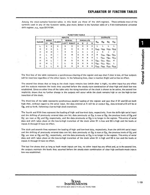
- Page 1 and 2: SDYD001TheTTLDataBookVolume!1984..
- Page 4 and 5: The TTL Data BookVolwne 1TEXASINSTR
- Page 8 and 9: The TTL Data Bool
- Page 11 and 12: 0 ••••••• 0 •••
- Page 13: , •••••••••••
- Page 20 and 21: 54174 FAMILIES OF COMPATIBLE TTL CI
- Page 22 and 23: GLOSSARYTTL SYMBOLS, TERMS, AND DEF
- Page 24 and 25: GLOSSARYTTL SYMBOLS, TERMS, AND DEF
- Page 28 and 29: The TTL Data- BookVolume 1General I
- Page 30 and 31: FUNCTIONAL INDEXGATES AND INVERTERS
- Page 32 and 33: FUNCTIONAL INDEXBUFFERS, DRIVERS, T
- Page 34 and 35: FUNCTIONAL INDEXLATCHES AND MULTIVI
- Page 36 and 37: FUNCTIONAL INDEXCOUNTERSSYNCHRONOUS
- Page 38 and 39: FUNCTIONAL INDEXDISPLAY DECODERS/DR
- Page 40 and 41: FUNCTIONAL INDEXMEMORIESUSER-PROGRA
- Page 42 and 43: The TTL Data BookVolume 1General In
- Page 44 and 45: PRODUCT GUIDEtypical performancelog
- Page 46 and 47: PRODUCT GUIDE06logic symboltHEX INV
- Page 48 and 49: PRODUCT GUIDE12TRIPLE 3-INPUTPOSITI
- Page 50 and 51: PRODUCT GUIDE18typical performance
- Page 52 and 53: PRODUCT GUIDE24logic symboltSCHMITT
- Page 54 and 55: PRODUCT GUIDElogic symbolt pin assi
- Page 56 and 57: PRODUCT GUIDE37 logic symboltQUADRU
- Page 58 and 59: PRODUCT GUIDE43typical performancel
- Page 60 and 61: PRODUCT GUIDEtypical performance lo
- Page 62 and 63: PRODUCT GUIDE544-WIDE AND-ORINVER
- Page 64 and 65: PRODUCT GUIDE57 logic symbol tGO-TO
- Page 66 and 67: PRODUCT GUIDE68DUAL 4-BIT DECADE CO
- Page 68 and 69: PRODUCT GUIDE72logic symbolt]'J~}pi
- Page 70 and 71: PRODUCT GUIDE75logic symbolt10ill-
- Page 72 and 73: PRODUCT GUIDE80GATED FULL ADDERSlog
- Page 74 and 75: PRODUCT GUIDE874-BIT TRUE/COMPLEMEN
- Page 76 and 77:
PRODUCT GUIDE93logic symbol, '93A,
- Page 78 and 79:
984-BIT DATA SELECTOR/STORAGE REGIS
- Page 80 and 81:
PRODUCT GUIDElogic symbol104tPRE~ 5
- Page 82 and 83:
PRODUCT GUIDE108DUAL J·K NEGATIVE
- Page 84 and 85:
PRODUCT GUIDElogic Iymbolt114DUAL J
- Page 86 and 87:
PRODUCT GUIDE123logic symboltpin as
- Page 88 and 89:
PRODUCT GUIDE128logic symboltLINE D
- Page 90 and 91:
PRODUCT GUIDEtypical performance lo
- Page 92 and 93:
PRODUCT GUIDE1383- TO 8-LINE DECODE
- Page 94 and 95:
PRODUCT GUIDElogic Iymboltpin assig
- Page 96 and 97:
PRODUCT GUIDElogic symbolt1511-0F-8
- Page 98 and 99:
PRODUCT GUIDElogic svmbolt1552-lIn.
- Page 100 and 101:
PRODUCT GUIDE1594· TO 16·LINE DEC
- Page 102 and 103:
PRODUCT GUIDE162SYNCHRONOUS 4-BITCO
- Page 104 and 105:
PRODUCT GUIDE167SYNCHRONOUS DECADER
- Page 106 and 107:
PRODUCT GUIDE17216-BIT REGISTER FIL
- Page 108 and 109:
PRODUCT GUIDE176 logic symbol, '176
- Page 110 and 111:
PRODUCT GUIDE182logic symbols tpin
- Page 112 and 113:
PRODUCT GUIDE185logic symboltpin as
- Page 114 and 115:
PRODUCT GUIDE192SYNCHRONOUS UP/DOWN
- Page 116 and 117:
PRODUCT GUIDE197PRESETTABLE BINARYC
- Page 118 and 119:
PRODUCT GUIDE219logic symboltpin as
- Page 120 and 121:
PRODUCT GUIDE225pin assignmentslogi
- Page 122 and 123:
PRODUCT GUIDE230,231OCTAL BUFFERS A
- Page 124 and 125:
PRODUCT GUIDE243logic symboltpin as
- Page 126 and 127:
PRODUCT GUIDElogic symbolt pin assi
- Page 128 and 129:
PRODUCT GUIDE251 logic symbolt pin
- Page 130 and 131:
PRODUCT GUIDE258 logic symbol, 'ALS
- Page 132 and 133:
PRODUCT GUIDE265 logic symbol tQUAD
- Page 134 and 135:
PRODUCT GUIDE278logic symbolt4-BIT
- Page 136 and 137:
PRODUCT GUIDE283logic symbolt}}{4-B
- Page 138 and 139:
PRODUCT GUIDE292 logic symboltPROGR
- Page 140 and 141:
PRODUCT GUIDE297 pin assignmentsDIG
- Page 142 and 143:
PRODUCT GUIDE319logic symbolt64-BIT
- Page 144 and 145:
PRODUCT GUIDE347 logic symbolt pin
- Page 146 and 147:
PRODUCT GUIDE351DUAL B·LINE TO 1·
- Page 148 and 149:
PRODUCT GUIDE355a·LINE TO 1·LINE
- Page 150 and 151:
PRODUCT GUIDE368 logic symbol tHEX
- Page 152 and 153:
PRODUCT GUIDE376logic symbol tpin a
- Page 154 and 155:
PRODUCT GUIDE382ARITHMETIC LOGIC UN
- Page 156 and 157:
PRODUCT GUIDE390DUAL DECADE COUNTER
- Page 158 and 159:
PRODUCT GUIDE412logic symboltpin as
- Page 160 and 161:
PRODUCT GUIDE436, 437 logic symbolt
- Page 162 and 163:
PRODUCT GUIDE440. 441,· 442. 443.
- Page 164 and 165:
PRODUCT GUIDE448QUAD TRIDIRECTIONAL
- Page 166 and 167:
PRODUCT GUIDE481pin assignmentsJ, N
- Page 168 and 169:
PRODUCT GUIDE484, 485 logic symbol
- Page 170 and 171:
PRODUCT GUIDE526FUSE PROGRAMMABLE 1
- Page 172 and 173:
PRODUCT GUIDE533OCTAL D-TYPE TRANSP
- Page 174 and 175:
PRODUCT GUIDE539 logic symbols t2-
- Page 176 and 177:
PRODUCT GUIDE560 logic symboltSYNCH
- Page 178 and 179:
I rPRODUCT GUIDE568logic symboltSYN
- Page 180 and 181:
PRODUCT GUIDEpin assignmentsJ. N PA
- Page 182 and 183:
PRODUCT GUIDElogic symbol t pin ass
- Page 184 and 185:
PRODUCT GUIDE594 logic symbolta-BIT
- Page 186 and 187:
PRODUCT GUIDE599 logic symbolta-BIT
- Page 188 and 189:
PRODUCT GUIDE602MEMORY REFRESHCONTR
- Page 190 and 191:
PRODUCT GUIDE608MEMORY CYCLECONTROL
- Page 192 and 193:
PRODUCT GUIDE620. 621622. 623OCTAL
- Page 194 and 195:
PRODUCT GUIDE627 typical performanc
- Page 196 and 197:
PRODUCT GUIDE632. 633logic diagram
- Page 198 and 199:
~PRODUCT GUIDE636, 6378-BIT PARALLE
- Page 200 and 201:
PRODUCT GUIDE640, 641, 642643, 644,
- Page 202 and 203:
PRODUCT GUIDE646, 647, 648, 649OCTA
- Page 204 and 205:
PRODUCT GUIDE651, 652logic symbol,
- Page 206 and 207:
PRODUCT GUIDE668, 669SYNCHRONOUS 4-
- Page 208 and 209:
PRODUCT GUIDE67316-BIT SHIFT REGIST
- Page 210 and 211:
PRODUCT GUIDE679, 680ADDRESS COMPAR
- Page 212 and 213:
PRODUCT GUiDE682, 683, 684, 685logi
- Page 214 and 215:
PRODUCT GUIDE688, 689logic symbol,
- Page 216 and 217:
PRODUCT GUIDE696, 697, 698, 699SYNC
- Page 218 and 219:
PRODUCT GUIDE758 logic symbol taUAD
- Page 220 and 221:
802logic symboltTRIPLE 4-INPUT ORIN
- Page 222 and 223:
PRODUCT GUIDE821logic symboltpin as
- Page 224 and 225:
PRODUCT GUIDE832logic symbol tHEX 2
- Page 226 and 227:
PRODUCT GUIDE846logic symbolt pin a
- Page 228 and 229:
PRODUCT GUIDE857HEX 2-TO-' UNIVERSA
- Page 230 and 231:
PRODUCT GUIDE870DUAL 16-BY-4 REGIST
- Page 232 and 233:
PRODUCT GUIDE873DUAL 4·BIT D·TYPE
- Page 234 and 235:
PRODUCT GUIDE878 logic symbol. 'ALS
- Page 236 and 237:
PRODUCT GUIDE882logic symboltpin as
- Page 238 and 239:
PRODUCT GUIDE890,891MICROSEQUENCERS
- Page 240 and 241:
PRODUCT GUIDE1000 logic Iymboltpin
- Page 242 and 243:
PRODUCT GUIDE1008 logic symboltQUAD
- Page 244 and 245:
PRODUCT GUIDE1034 logic symbolt pin
- Page 246 and 247:
PRODUCT GUIDE1243 logic symboltQUAD
- Page 248 and 249:
PRODUCT GUIDE1620, 1621, 1622, 1623
- Page 250 and 251:
PRODUCT GUIDE1640, 1641, 1642,1643,
- Page 252 and 253:
PRODUCT GUIDE2620,2623 pin assignme
- Page 254 and 255:
PRODUCT GUIDE8003 logic symboltDUAL
- Page 256 and 257:
PRODUCT GUIDE'PAL16R6FIELD-PROGRAMM
- Page 258 and 259:
~PRODUCT GUIDE'PAL20R6FIELD·PROGRA
- Page 260 and 261:
PRODUCT GUIDE'PALR19L8FIELD-PROGRAM
- Page 262 and 263:
PRODUCT GUIDE'PALT19L8FIELD-PROGRAM
- Page 264 and 265:
PRODUCT GUIDETBP14510 ('5287) This
- Page 266 and 267:
PRODUCT GUIDETBP24841 (,5476)logic
- Page 268 and 269:
PRODUCT GUIDETBP28l42logic symbol t
- Page 270 and 271:
PRODUCT GUIDETBP28L165logic symbolt
- Page 272 and 273:
PRODUCT GUIDETBP28SA42logic symbolt
- Page 274 and 275:
PRODUCT GUIDETBP28SA86APROGRAMMABLE
- Page 276 and 277:
The TTL Data BookVolume 1General In
- Page 278 and 279:
EXPLANATION OF NEW LOGIC SYMBOLSTAB
- Page 280 and 281:
EXPLANATION OF NEW LOGIC SYMBOLSby
- Page 282 and 283:
EXPLANATION OF NEW LOGIC SYMBOLSA c
- Page 284 and 285:
EXPLANATION Of NEW LOGIC SYMBOLSTAB
- Page 286 and 287:
EXPLANATION OF NEW LOGIC SYMBOLSThe
- Page 288 and 289:
EXPLANATION OF NEW LOGIC SYMBOLSIn
- Page 290 and 291:
=[ --a c
- Page 292 and 293:
EXPLANATION OF NEW LOGIC SYMBOLS4.7
- Page 294 and 295:
EXPLANATION OF NEW LOGIC SYMBOLSWhe
- Page 296 and 297:
EXPLANATION OF NEW LOGIC SYMBOLSIn
- Page 298 and 299:
EXPLANATION OF NEW LOGIC SYMBOLSIf
- Page 300 and 301:
EXPLANATION OF NEW LOGIC SYMBOLS6 C
- Page 302 and 303:
EXPLANATION OF NEW LOGIC SYM~OLS8 U
- Page 304 and 305:
EXPLANATION OF NEW LOGIC SYMBOLSSym
- Page 306 and 307:
The TTL Data Book. Volume 1General
- Page 308 and 309:
MECHANICAL DATAORDERING INSTRUCTION
- Page 310 and 311:
MECHANICAL DATAFH and FK ceramic ch
- Page 312 and 313:
MECHANICAL DATAJG ceramic dual-in-I
- Page 314 and 315:
MECHANICAL DATAJ ceramic dual-in-Ii
- Page 316 and 317:
MECHANICAL DATAceramic packages - s
- Page 318 and 319:
MECHANICAL DATAN plastic dual-in-li
- Page 320 and 321:
28-PIN N PLASTIC,e 36,6 (1.440) MAX
- Page 322 and 323:
MECHANICAL DATAP plastic dual-in-li
- Page 324 and 325:
NOTES
- Page 326 and 327:
NOTES
- Page 328 and 329:
NOTES
- Page 330 and 331:
NOTES
- Page 332 and 333:
NOTES
- Page 334 and 335:
NOTES
- Page 336 and 337:
Tl Sales OfficesALABAMA: Hunllville
- Page 339:
Printed in U.S.A.Creating useful pr