Power Reduction Techniques for LDPC Decoders
Power Reduction Techniques for LDPC Decoders
Power Reduction Techniques for LDPC Decoders
You also want an ePaper? Increase the reach of your titles
YUMPU automatically turns print PDFs into web optimized ePapers that Google loves.
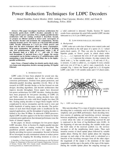
IEEE TRANSACTIONS ON VERY LARGE SCALE INTEGRATION SYSTEMS 1<strong>Power</strong> <strong>Reduction</strong> <strong>Techniques</strong> <strong>for</strong> <strong>LDPC</strong> <strong>Decoders</strong>Ahmad Darabiha, Student Member, IEEE, Anthony Chan Carusone, Member, IEEE, and Frank R.Kschischang, Fellow, IEEEAbstract—This paper investigates hardware architectures <strong>for</strong>low-density parity-check (<strong>LDPC</strong>) decoders amenable to lowvoltageand low-power operation. First, a highly-parallel decoderarchitecture with low routing overhead is described. Second,we propose an efficient method to detect early convergence ofthe iterative decoder and terminate the computations, therebyreducing dynamic power. We report on a bit-serial fully-parallel<strong>LDPC</strong> decoder fabricated in a 0.13-µm CMOS process andshow how the above techniques affect the power consumption.With early termination, the prototype is capable of decodingwith 10.4 pJ/bit/iteration, while per<strong>for</strong>ming within 3 dB ofthe Shannon limit at a BER of 10 −5 and with 3.3 Gbpstotal throughput. If operated from a 0.6-V supply, the energyconsumption can be further reduced to 2.7 pJ/bit/iteration whilemaintaining a total throughput of 648 Mbps, due to the highlyparallelarchitecture.Index Terms—Channel coding, low-density parity-check codes,very-large-scale integration, iterative message passing, 10 GigabitEthernet.I. INTRODUCTION<strong>LDPC</strong> codes [1] have been adopted <strong>for</strong> several new digitalcommunication standards due to their excellent errorcorrection per<strong>for</strong>mance, freedom from patent protection, andinherently-parallel decoding algorithm [2]–[4]. Most of theresearch on <strong>LDPC</strong> decoder design so far has focused on codedesigns, decoding algorithms, and decoder architectures thatimprove decoder throughput. Fewer papers have discussedlow-power architectures <strong>for</strong> <strong>LDPC</strong> decoders. Analog decodershave been proposed <strong>for</strong> low-power decoding of <strong>LDPC</strong> [5]and Turbo codes [6]. However, analog decoders have onlybeen demonstrated on codes with block lengths less than 250bits. Scaling analog decoders to longer block lengths will becomplicated by device mismatches and the need to store andbuffer hundreds of analog inputs to the decoder. The per<strong>for</strong>manceof such short block-length codes is insufficient <strong>for</strong> thetargeted applications, and the throughput of analog decoders islimited to less than 50 Mbps. In nanoscale CMOS processes,digital <strong>LDPC</strong> decoders appear to be the best solution <strong>for</strong> futurecommunication applications that demand per<strong>for</strong>mance near thelimits of channel capacity.In this paper, we discuss techniques <strong>for</strong> low-power digital<strong>LDPC</strong> decoders. First, in Section II a highly-parallel decoderarchitecture with low routing overhead is described. Theparallelism permits operation from a low supply voltage,thereby providing low-power consumption. Second, in SectionIII we investigate an early termination scheme to reduce powerconsumption by stopping the decoding iterations as soon asA. Darabiha, A. Chan Carusone and F. R. Kschischang are with The EdwardS. Rogers Sr. Department of Electrical and Computer Engineering, Universityof Toronto, Toronto M5S 3G4, Canada (email: ahmadd@eecg.utoronto.ca;tcc@eecg.utoronto.ca; frank@comm.utoronto.ca).a valid codeword is detected. Finally, Section IV reportsresults from a prototype bit-serial fully-parallel <strong>LDPC</strong> decoderfabricated in a 0.13-µm CMOS process.A. BackgroundII. LOW-POWER PARALLEL DECODERS<strong>LDPC</strong> codes are a sub-class of linear error control codes andcan be described as the null space of a sparse {0, 1}−valuedparity-check matrix, H. They can also be described by abipartite graph, or Tanner graph, in which check nodes{c 1 , c 2 , . . . , c C } represent the rows of H and variable nodes{v 1 , v 2 , . . . , v V } represent the columns. An edge connects thecheck node c m to the variable node v n if and only if H mnis nonzero. A code is called (d v , d c )-regular if every columnand every row of H has d v and d c ones, respectively. As anexample, Fig. 1 shows the Tanner graph <strong>for</strong> a (3, 6)-regular<strong>LDPC</strong> code with V =10 variable nodes and C=5 check nodes.Fig. 1.c 1c 2c 3c 4c 5from channelchecknodesv 1v 2v 3v 4v 5v 6v 7v 8 v 9v 10<strong>LDPC</strong> code Tanner graph.variablenodesMin-sum decoding [7] is a type of iterative message-passingdecoding that is commonly used in <strong>LDPC</strong> decoders due to itssimplicity and good BER per<strong>for</strong>mance. Each decoding iterationconsists of updating and transferring extrinsic messagesbetween neighboring variable and check nodes. A message isa belief about the value of corresponding received bit andis expressed in the <strong>for</strong>m of log-likelihood ratio (LLR). Atthe beginning of min-sum decoding, the variable nodes passthe LLR value of the received symbols (i.e. the intrinsicmessage) to all the neighboring check nodes. Then eachiteration consists of check update phase followed by variableupdate phase. During the check update phase the outgoingmessage on each edge of the check node is calculated as afunction of the incoming messages from all the other edges:the magnitude of the output is the minimum of the inputmagnitudes and the sign is the parity of the signs of the inputs.During the variable update phase the outgoing message on
IEEE TRANSACTIONS ON VERY LARGE SCALE INTEGRATION SYSTEMS 3while maintaining the same throughput: f 2 = f 1 /k. Since weare striving <strong>for</strong> low-power operation, each decoder operatesfrom the lowest supply voltage that will support its targetedclock frequency. Hence, the parallel design can be operatedfrom a lower supply voltage (V dd2 ) than the reference design(V dd1 ). Following an analysis similar to [10], we have V dd2 =v sc V dd1 , wheredissipation when operating at the maximum clockfrequency and with typical supply voltage values.This is also consistent with the power measurementsreported in [11].b) The overhead associated with the increased parallelismis negligible. This is the focus of SectionII.C.v sc = m +(1 − m)22k+√ (m +) 2(1 − m)2− m2k2 (1)and m = V t /V dd1 . There<strong>for</strong>e, the power savings offered bythe parallel design isP 2 = v2 sck (1 + β(k − 1)) P 1 ≡ ηP 1 , (2)Fig. 4(a) shows the normalized supply voltage, v sc , required<strong>for</strong> different values of k to maintain a constant throughputbased on (1) <strong>for</strong> a typical 0.13-µm CMOS process whereV t = 0.3V and V dd1 = 1.2V . Fig. 4(b) shows the normalizedpower, η, versus the parallelism factor, k, <strong>for</strong> different valuesof β based on (2). It can be seen that the power reductionis greatest <strong>for</strong> small values of β since in those cases C mis the dominant portion of C 1 , so added parallelism impliesa negligible increase in the system’s effective capacitance.However, significant power savings can be achieved even withhigh values of β. For example, with β = 0.95 and k = 4 thesupply voltage can be reduced by about 50%, resulting in a74% power saving compared with the reference design.Normalized supply voltage, v sc10.90.80.70.60.50.40.30.20.102 4 6 8 10Parallelism, k(a)Normalized power, η10.90.80.70.60.50.40.30.20.10β=0.95β=0.50β=0.052 4 6 8 10Parallelism, k(b)Fig. 4. <strong>Power</strong> reduction as a result of a parallel architecture: a) <strong>Reduction</strong>in supply voltage. b) <strong>Reduction</strong> in dynamic power dissipation.The preceding analysis makes two assumptions that havenot, yet, been discussed:a) <strong>Power</strong> consumption is dominated by dynamicpower dissipation. Our measurements <strong>for</strong> the decoderpresented this work suggest that leakagepower constitutes less than 1% of the total powerC. A fully-parallel decoder with bit-serial message passingFollowing the power efficiency discussion above, we haveadopted a fully-parallel architecture where a separate VNUor CNU is designated <strong>for</strong> each variable node or check nodein the code Tanner graph. Another advantage of fully-paralleldecoder architecture is that unlike most partially-parallel decodersthat are based on a particular code construction (suchas the (3, k)-regular construction in [12], or the Architecture-Aware code construction in [13]), the fully-parallel architecturecan be applied to irregular codes with no constraint on thecode structure. This is done simply by instantiating VNUsand CNUs of the desired degree and connecting them basedon the code graph. The only consideration is that the timingper<strong>for</strong>mance of the decoder <strong>for</strong> irregular codes will be typicallylimited by a critical path through the nodes with highestdegree.Fig. 5 shows the high-level architecture of the 0.13µm-CMOS bit-serial <strong>LDPC</strong> decoder implemented in this work.The decoder is based on a (4, 15)-regular <strong>LDPC</strong> code withV = 660 variable nodes and C = 176 check nodes. This codewas constructed using a progressive edge-growth algorithm[14] that minimizes the number of short cycles in the code’sTanner graph. It can be seen that the extrinsic memory blockof Fig. 2 is replaced with the interconnections. This is becausein a fully-parallel architecture each extrinsic message is onlywritten by one VNU or CNU, so the extrinsic memory cannow be distributed amongst VNUs and CNUs and no addressgeneration is needed.The major challenge in implementing highly-parallel decoders[11] is the large area and the overhead effects such asthe routing complexity that are not modeled in the discussionin Section II.B. To reduce the effect of routing complexity,we have used a bit-serial message-passing scheme in thiswork where multi-bit messages are communicated between thenodes over multiple clock cycles [15]. In addition to reducingthe routing complexity, the bit-serial message-passing requiresless logic to per<strong>for</strong>m min-sum <strong>LDPC</strong> decoding because boththe MIN and SUM operations are inherently bit-serial. Asa result, bit-serial VNUs and CNUs can be efficiently implementedto generate only partial 1-bit extrinsic messagesevery clock cycle. Although bit-serial message-passing reducesthe amount of global wiring, the routing complexity willeventually limit the maximum length of the <strong>LDPC</strong> codesthat can be implemented in a bit-serial fully-parallel decoder.However, the important point is that the bit-serial schemepushes the practical code length limit to higher values, makingit feasible to implement fully-parallel decoders <strong>for</strong> emerginghigh-speed standards such as 10GBase-T or Mobile WiMAXwhich specify code lengths of 2048 and 2304, respectively.
IEEE TRANSACTIONS ON VERY LARGE SCALE INTEGRATION SYSTEMS 4The decoder in this work per<strong>for</strong>ms an approximate min-sumdecoding algorithm that reduces the area of the CNUs by morethan 40% compared with conventional min-sum decodingwith only a 0.1dB per<strong>for</strong>mance penalty at BER=10 −6 [15].Fig. 6 shows the CNU schematic where the inputs and outputsare communicated bit-serially in sign-magnitude MSB-first<strong>for</strong>mat. The top section of the schematic is <strong>for</strong> calculatingthe output magnitudes as in [15] and the lower block inthe figure calculates the output sign using an XOR-tree. TheVNU logic in min-sum decoding must take the sum of all itsinputs. Unlike the CNUs, the SUM operations in the VNUsare more efficiently per<strong>for</strong>med <strong>for</strong> inputs in LSB-first 2’scomplement <strong>for</strong>mat. So, the message <strong>for</strong>mats are convertedaccordingly at the output of VNUs and CNUs. Convertingbetween LSB-first and MSB-first bit-serial communicationrequires additional registers to store the messages. However,these registers are already present in the CNUs and VNUs<strong>for</strong> the block interleaving as explained below. The design hasa core utilization of 72%, compared with 50% in the fullyparallel<strong>LDPC</strong> decoder reported in [11] that does not employbit-serial message passing. The high utilization implies thatthere is little routing overhead associated with the decoder’sparallelism.The timing diagram of the decoder is shown in Fig. 7. Inthis decoder, 4-bit quantized LLR messages are transferredbetween VNUs and CNUs bit-serially in 4 clock cycles. Asa result, each decoding iteration takes 4 clock cycles in thecheck node and 4 cycles in the variable node. After every 4cycles, the variable and check nodes swap messages, allowingtwo different frames to be simultaneously decoded in aninterleaved fashion.Chk_in(1)Bit-serialcheck nodeinputsFig. 6.Chk_in(d c )Sign/MagInputbufferDecoderOutputbufferQ(1)Q(d c)Q(1)Q(d c)‘001’Unique minimumdetectionXOR-outSign calculations(1)s(d c)MinMin+1Statusflagss(1)s(d c)The CNU schematic <strong>for</strong> approximate min-sum decoding.Frame # n-215 iterationsFrame # n Frame # n+1 Frame # n+2 Frame # n+3Frame # n-3Frame # n-1Frame # n-2Frame # n(a)Frame # n-1Frame # n+1Frame # n+2Frame # nCheck_out(1)Sign/MagBit-serialcheck nodeoutputsCheck_out(d c )Sign/MagFromchannelIntrinsicmemoryOutputbufferVNUsVNU 1VNU 2Interconnections(# of edges = 2Cd c= 2Vd v)CNUsCNU 1CNU CVNU VCNU 2Fig. 7.CLKCheck nodeVariablenodeFrame # nFrame #n+11 iteration4 cycles# n+1# n(b)# n# n+1# n+1# nTiming diagram <strong>for</strong> block-interlaced bit-serial decoding.Fig. 5.DecodedbitsControlThe fully-parallel iterative <strong>LDPC</strong> decoder architecture.Section IV will report the measured timing and powerper<strong>for</strong>mance of the implemented decoder. It will show howvoltage scaling can be used to trade high throughput <strong>for</strong> lowpowerdecoding. Even without the techniques described in thenext section, voltage scaling results in an energy efficiency of7.4 pJ/bit/iter at 648 Mbps throughput which is lower than thebest previously-reported digital and analog iterative decoders[11] [5].III. <strong>LDPC</strong> DECODING WITH EARLY TERMINATIONA. Background<strong>LDPC</strong> decoders generally correct most bit errors within thefirst few decoding iterations. Subsequent iterations provide diminishingincremental improvements in decoder per<strong>for</strong>mance.The number of iterations per<strong>for</strong>med by the decoder, I M , is usuallydetermined a priori and hard-coded based on worst-casesimulations. There<strong>for</strong>e, the decoder per<strong>for</strong>ms I M iterationseven though it will usually converge to its final output muchsooner. We propose a decoder architecture that automaticallydetects when it has converged to its final output and shuts offall VNUs and CNUs <strong>for</strong> the remainder of each frame to savepower.
IEEE TRANSACTIONS ON VERY LARGE SCALE INTEGRATION SYSTEMS 5Earlier work in this area has focused on identifying particularbits within each frame that appear likely to haveconverged [16], [17]. They have suggested that one can stopupdating extrinsic messages <strong>for</strong> those reliable bits while otherunreliable bits are still being decoded. The resulting powersavings depends on the specific criteria used to identify the reliablebits. Un<strong>for</strong>tunately, these bits are sometimes incorrectlyidentified, so the decoder’s per<strong>for</strong>mance suffers. In [18], anadditional post-processing decoder is introduced to mitigatethis per<strong>for</strong>mance degradation. Naturally, there is overheadassociated with identifying the reliable bits and with the postprocessingdecoder. The overhead reduces the potential powersavings of this approach.In this work, instead of trying to identify individual bitsthat appear to have converged early, we monitor the entireframe to determine when the decoder has converged to avalid codeword. We then deactivate the entire decoder <strong>for</strong>the remaining iterations to save power. The remainder of thissection describes a hardware-efficient implementation of thistechnique with significant power savings and no per<strong>for</strong>mancedegradation.B. Early terminationAlthough EXIT charts can be used to determine the averagenumber of iterations required <strong>for</strong> convergence of an <strong>LDPC</strong>decoder operating on very long block lengths [19], <strong>for</strong> practicalblock lengths of 1000 to 10,000 bits the estimates so obtainedare inaccurate. Instead, we have used extensive simulations toinvestigate the convergence behavior of two practical <strong>LDPC</strong>codes.Fig. 8 shows the BER versus input SNR <strong>for</strong> two different<strong>LDPC</strong> codes under 4bit-quantized min-sum decoding. Thecode in Fig. 8(a) is the Reed-Solomon based (6, 32)-regular2048-bit <strong>LDPC</strong> code as specified <strong>for</strong> the 10Gigabit Ethernetstandard [2], while the code in Fig. 8(b) is the same codeemployed in the hardware prototype described in Section II.Each code is simulated with different number of iterations, I M .These simulations indicate that little per<strong>for</strong>mance improvementis observed <strong>for</strong> either code as the number of iterationsis increased from I M = 12 to I M = 16. There<strong>for</strong>e, no morethan I M = 16 iterations are required <strong>for</strong> either code.The convergence behavior of the same two codes is shownin Fig. 9 which plots the average fraction of uncorrectedframes versus the iteration number. These two figures showthat the vast majority of frames are correctly decoded in thefirst few iterations. For example, <strong>for</strong> the code in Fig. 9(a), atan Eb/No of 5.1 dB more than 99.99% of all frames havebeen successfully decoded during the first 5 iteration.Fig. 10 plots the ratio of the average number of requirediterations to I M , α, versus input SNR <strong>for</strong> the same twocodes as in Fig. 9. The figure shows the graphs <strong>for</strong> I M =4,8, 12 and 16. For example, based on Fig. 10(b), <strong>for</strong> thecode implemented in this work with I M = 15, on averageless than 3 iterations are needed per frame at SNR=4.3dB(corresponding to BER=10 −5 ). As will be shown in the resultssection, by exploiting this behavior and turning off the decoderin the remaining un-needed iterations the total dynamic poweris reduced by 65%.BER10 -2 4 iter8 iter12 iter10 -316 iter10 -410 -510 -610 -710 -84 4.5 5 5.5Eb/N0 (dB)(a)BER10 -2 4 iter8 iter10 -312 iter16 iter10 -410 -510 -610 -710 -84 4.5 5 5.5Eb/N0 (dB)Fig. 8. BER vs. maximum number of iterations under 4-bit quantized minsumdecoding: (a) Reed-Solomon based (6, 32)-regular 2048-bit code and (b)PEG (4, 15)-regular 660-bit code.Fraction of uncorrected framesEBNo=4.5 dBEBNo=5.1 dB10 -1 EBNo=5.7 dB10 -210 -310 -410 -510 -60 5 10 1510 0 Iterations(a)Fraction of uncorrected frames(b)10 010 -110 -210 -310 -410 -5IterationsEBNo=4.0 dBEBNo=4.5 dBEBNo=4.9 dB10 -60 5 10 15Fig. 9. The fraction of uncorrected frames vs. iteration number <strong>for</strong> (a) aReed-Solomon based (6, 32)-regular 2048-bit code, (b) a PEG (4, 15)-regular660-bit code.C. Hardware ImplementationThe remaining task is to efficiently implement early terminationin hardware. In other words, to detect that the decoderhas converged to a correct codeword. A standard approach is tomake final decisions in each VNU at the end of each iterationand then check if all parity constraints are satisfied. This isreferred to as syndrome checking. Although straight<strong>for</strong>ward,this approach has a considerable hardware cost <strong>for</strong> two reasons.First, it requires additional hardware in the VNUs tomake the hard decisions at the end of each iteration. Second,the hard decisions must be distributed to the destination check(b)
IEEE TRANSACTIONS ON VERY LARGE SCALE INTEGRATION SYSTEMS 6Average ratio of active iterations, α10.90.80.70.60.50.40.30.20.1I M= 4I M= 8I M= 12I M= 16Average ratio of active iterations, α10.90.80.70.60.50.40.30.20.1I M= 4I M= 8I M= 12I M= 16FromchannelIntrinsicmemoryOutputbufferDecodedbitsVNUsCNUsENENENVNU 1VNU 2InterconnectionsControlCNU 1CNU 2ENCNU CVNU VENENCheck_enableVariable_enableXOR_outOR treeEnablelogicClkNew_frameReset04 4.5 5 5.5Eb/N0 (dB)(a)04 4.5 5Eb/N0 (dB)(b)Fig. 11. The fully-parallel iterative <strong>LDPC</strong> decoder with early terminationfunctionality.Fig. 10. Ratio of active iterations (a) Reed-Solomon based (6, 32)-regular2048-bit code and (b) PEG (4, 15)-regular 660-bit code.Evenframes# n-2I Miterations# n# n+2nodes in every iteration where syndrome checking can beper<strong>for</strong>med. This distribution can be done either by dedicatingextra hard wires from VNUs to the neighboring CNUs, orby sharing the same wires used <strong>for</strong> transferring extrinsicmessages in a bit-serial time multiplexed fashion. But neitherof these approaches are efficient because they either increasethe routing complexity by adding global wires or decreasedecoding throughput by increasing the number of clock cyclesper iteration.Alternatively, in this work we check the parity of the normalvariable-to-check messages that are already required by thedecoding iterations. If the parity of all these messages are satisfied,we stop decoding <strong>for</strong> that frame and compute the finalhard decision at the beginning of next iteration. Although notmathematically equivalent to the standard syndrome checking,we have simulated the two <strong>LDPC</strong> codes of Fig. 8 with the sameset of 10 6 frames both without and with early termination atEb/No ranging from 4 dB to 5.1 dB. The simulations showidentical per<strong>for</strong>mance between the two approaches <strong>for</strong> thesecodes.For the two codes discussed in this paper, our method onaverage needs one extra iteration to terminate compared withthe conventional syndrome checking method. This differencereduces the amount of power savings achieved compared tothe conventional syndrome checking. For example, in the 660-bit decoder presented in Section II.C, conventional syndromechecking could have improved the percentage of power savingsfrom 49% to 51% <strong>for</strong> low-SNR inputs (Eb/No ≈ 3 dB) andfrom 66% to 72% <strong>for</strong> high-SNR inputs (Eb/No ≈ 6 dB).In spite of the reduced power savings, we have adopted thisnew termination method <strong>for</strong> two reasons. First, in contrast toconventional early termination our termination method doesnot increase the number of VNU-to-CNU wires, nor does itrequire extra clock cycles per iteration to distribute the harddecision results to the CNUs. Second, this approach requiresminimal hardware overhead since most of the calculations arealready part of the normal VNU and CNU operations.OddframesEvenframesOddframesOR-treeoutput# n-2# n-1# n-1# n(a)I Miterations(b)# n+1# n+1# n+2Fig. 12. Block-interlaced decoding timing diagram (a) without earlytermination, (b) with early termination.Fig. 11 shows the block diagram of a decoder with earlytermination logic. It is similar to the one in Fig. 5 with afew added blocks: First, all the parity results are ORed. Theoutput of the OR tree is zero only when all the paritiesare satisfied. Second, a termination logic block generatesthe proper disable/enable signals <strong>for</strong> the VNUs and CNUsdepending on the value of the OR tree output. If the output ofthe OR tree is zero, it keeps the VNUs and CNUs disabled <strong>for</strong>the remaining iterations. Fig. 12 shows the timing diagrams ofthe decoder, with and without early termination. It shows thatthe decoding throughput is the same in both cases since thestart time <strong>for</strong> decoding the frames is identical. However thepower consumption is reduced in Fig. 12 because the decoderis turned off as soon as a correct codeword is detected.The synthesis results show that the added OR tree and theenable/disable functionality required in CNUs and VNUs addsonly less than 0.1% and 0.5% to the total decoder gate count,respectively. It should also be noted that no additional logic isrequired inside the CNUs to generate the XOR-out signals as
IEEE TRANSACTIONS ON VERY LARGE SCALE INTEGRATION SYSTEMS 7Control pins300ExtrapolatedMeasured1500ExtrapolatedMeasured3 mm44inputpins660VNUs&176CNUs44outputpinsMax. Frequency (MHz)250200150100<strong>Power</strong> (mW) (@ max. frequency)10005003 mm500.6 0.8 1 1.2V dd(V)00.6 0.8 1 1.2V dd(V)Fig. 13.Decoder die photo.<strong>Power</strong> (mW) (300 MHz, 1.2V)Fig. 14.16001200800400No early terminationWith early termination02 3 4 5 6 7 8Eb/No (dB)Decoder power consumption vs. input SNR.this value is already available from the sign-calculation blockinside the CNUs (Fig. 6).IV. RESULTSFig. 13 shows the die photo of the implemented decoder.The decoder per<strong>for</strong>ms 15 decoding iterations per frame as itwas shown in Fig. 8(b) that per<strong>for</strong>ming more than 12 iterationsresults in a negligible BER enhancement. It occupies 7.3 mm 2core area and operates at maximum frequency of 300 MHzwith a 1.2-V core supply voltage which results in a 3.3 Gbpstotal throughput. Since the code rate is 0.74, this correspondsto an in<strong>for</strong>mation throughput of 2.44 Gbps. The measuredBER per<strong>for</strong>mance of the decoder matches bit-true simulations.The BER curve is practically identical to the BER graph inFig. 8(b) <strong>for</strong> I M = 16.The total decoder power consumption is shown in Fig. 14as a function of input SNR at 300 MHz with 1.2-V supplyvoltage. The solid line in this graph is directly obtained frommeasurements. It was observed that approximately 20% of thetotal power dissipation is due to the clock tree. It was alsoFig. 15. Effect of supply voltage scaling on maximum frequency and powerconsumption.observed that only less than 1.4 mW (i.e., 0.1% of the totalpower consumption) is due to leakage current. The graph inFig. 14 also shows that in contrast to the fully-parallel <strong>LDPC</strong>decoder in [11], the power consumption is relatively flat <strong>for</strong> theSNR values of interest in this work. This is mostly becauseof the bit-serial message-passing and the block interleavingarchitecture which tend to maintain high switching activityindependent of the input SNR.The power consumption resulting from early termination asproposed in this work is shown by the dotted line in Fig. 14.Since early termination logic was not included in the fabricatedprototype, we have calculated the P D ′ data points on the dottedline from the P D data points on the solid line usingP ′ D = (1 + γ)(p c + α(1 − p c ))P D ,where γ accounts <strong>for</strong> the overhead of the early terminationlogic, p c is the fraction of dynamic power attributable to theclock tree, and α is the ratio of active iterations similar tothe values plotted in Fig. 10(b). This expression accounts <strong>for</strong>the fact that early termination does not decrease the dynamicpower in the clock tree. As explained in Section III, γ <strong>for</strong> thereported decoder is estimated to be less than 0.006. As alsomentioned, our measurements show that p c is approximately0.2. The figure shows that early termination reduces the powerconsumption by between 58% and 66% in the practical SNRrange of interest between Eb/No=4 dB and Eb/No=5.5 dB.Fig. 15 shows the effect of supply-voltage scaling on themeasured maximum frequency and the total power dissipationat that frequency. The dotted lines are the predicted valuesbased on the MOS square-law equation with V t = 0.3V .It can be seen that the measured results closely follow thepredicted results both <strong>for</strong> maximum frequency and <strong>for</strong> thepower consumption.Table I summarizes the characteristics of the fabricateddecoder. In Table II the results from other <strong>LDPC</strong> decodersreported in literature are listed. The decoder architecture in
IEEE TRANSACTIONS ON VERY LARGE SCALE INTEGRATION SYSTEMS 8TABLE ICHARACTERISTICS SUMMARY AND MEASURED RESULTS.Process0.13-µm CMOSArchitectureBit-serial fully-parallelCode constructionRegular 660-bitCode rate 0.74Decoding algorithmModified min-sumTotal area 9mm 2Core area 7.3mm 2Gate count690 kCore area utilization 72%Iterations per frame 15Message word length4 bitsPackageQFP160Supply voltage 1.2 V 0.6 VMaximum frequency (MHz) 300 59Total throughput (Mbps) 3300 648In<strong>for</strong>mation throughput (Mbps) 2440 480Early termination No Yes No Yes<strong>Power</strong> @ (Eb/No=4dB) (mW) 1408 518 72 26.5<strong>Power</strong> @ (Eb/No=5.5dB) (mW) 1383 398 71 20.5Energy (pJ/bit/iter) (@ Eb/No=4dB) 28.5 10.4 7.4 2.7Energy (pJ/bit/iter) (@ Eb/No=5.5dB) 27.9 8.0 7.3 2.1[11] is fully parallel, whereas the decoders in [20] and [21]are partially parallel. The power and throughput per<strong>for</strong>mancecomparison between these works is shown in Fig. 16. To takeinto account the varying number of iterations per frame and thedifferent code rates in the different decoders, the throughputon the vertical axis is the in<strong>for</strong>mation throughput normalizedto a maximum of 15 iterations per frame, which is usedin our decoder. The horizontal axis is the energy efficiencyof the decoder in pJ per bit per iteration. This value isobtained by dividing the decoder power consumption by totaldecoder throughput and the number of iterations per frame. Forcomparison purposes, we have also included scaled values <strong>for</strong>area, throughput and energy efficiency in Table II and Fig. 16.The area entries in the brackets in Table II are scaled downquadratically to a 0.13-µm CMOS process and also scaledlinearly to a block length of 660 bits. The throughputs andenergy efficiencies are scaled linearly and cubically to 0.13-µm CMOS process, respectively (Ref. [22], Chapter 16). Thecomparison graph confirms that fully-parallel decoders providebetter energy efficiency and decoding throughput compared tomemory-based partially-parallel decoders.The high energy efficiency in [11] can be attributed to itshigh level of parallelism as predicted in this paper. It canalso be explained with the fact that even though the decoderper<strong>for</strong>ms 64 iterations on each block, the vast majority ofblocks converge in the first few iterations, resulting in minimalswitching activity <strong>for</strong> the remaining iterations. This is incontrast with the bit-serial block-interlaced decoder presentedin our work where the switching activity does not scale downwith decoder convergence unless an early termination methodis applied. Finally, the average variable node degree in [11] is3.25 compared to the average degree of 4 in our decoder. Fortwo decoders with the same code length and the same coderate, the decoder with lower average node degree computesless messages in each iteration, and hence, consumes lesspower.One important dimension which is missing from Fig. 16is the decoder total silicon area and its routing complexity.For example, although the fully-parallel decoder in [11] hasgood power and throughput per<strong>for</strong>mance, its large area makesit very costly in practice. The bit-serial fully-parallel schemedemonstrated in this work combined with the early terminationscheme reduces routing complexity and area while maintainingthe throughput and energy efficiency advantages of fullyparalleldecoders. Compared to conventional fully-paralleldecoders, the logic area is reduced in bit-serial fully-paralleldecoders because only 1-bit partial results are generated ineach clock cycle. In addition, the reduced routing congestionallows <strong>for</strong> higher area utilization. This can be observed fromthe 52.5 mm 2 total area (18.1 mm 2 , if scaled <strong>for</strong> process andcode length) with about 50% area utilization in [11] comparedto the 9mm 2 total area with 72% area utilization in our design.With the power reduction achievable by early termination,the decoder consumes only 10.4 pJ/bit/iteration from 1.2Vsupply voltage and has a total throughput of 3.3 Gbps. Theprojected lines in the graph show that even further powerreductions are achievable if supply voltage scaling is combinedwith early termination. A minimum of 2.7 pJ/bit/iteration ispredicted with a 0.6-V supply voltage operating at 59 MHz andproviding 648 Mbps total throughput. These energy efficiencyresults even compare favorably with analog decoders which areaimed <strong>for</strong> energy efficiency. For example, the analog <strong>LDPC</strong>decoder reported in [5] consumes 0.83 nJ/bit (compared to lessthan 0.43 nJ/Bit in this work) with and has a throughput ofonly 6 Mbps .V. CONCLUSIONWe have discussed two techniques to improve the powerefficiencyof <strong>LDPC</strong> decoders. First, we analyzed how theincreased parallelism coupled with a reduced supply voltageis a particularly effective technique to reduce the power consumptionof <strong>LDPC</strong> decoders due to their inherent parallelism.Second, we proposed a scheme to efficiently implement earlytermination of the iterative decoding to further reduce thepower consumption. In spite of their superior speed and energyefficiency, it is known that their large area and complexinterconnect network limit the scalability of conventionalfully-parallel <strong>LDPC</strong> decoders [11]. The bit-serial fully-parallelarchitecture proposed in this work addresses these concernsby reducing both interconnect complexity and logic area. Itis preferable to memory-based partially-parallel architectures<strong>for</strong> applications such as 10GBase-T which use medium-size<strong>LDPC</strong> code (e.g., 2048 bit) and require multi-Gbps decodingthroughput. We reported on a fabricated 0.13-µm CMOS bitserialfully-parallel <strong>LDPC</strong> decoder and show the effect of theproposed techniques. The decoder has a 3.3 Gbps throughputwith a nominal 1.2-V supply and per<strong>for</strong>ms within 3 dB of theShannon limit at a BER of 10 −5 . With more than 60% powersaving achieved by early termination, the decoder consumes10.4 pJ/bit/iteration at Eb/No=4dB. Coupling early terminationwith supply voltage scaling results in even lower consumptionof 2.7 pJ/bit/iteration with 648 Mbps total decoding throughput.
IEEE TRANSACTIONS ON VERY LARGE SCALE INTEGRATION SYSTEMS 9TABLE IICOMPARISON WITH OTHER WORKS.[11] [20] [21]Process 0.16-µm CMOS 0.18-µm CMOS 0.18-µm CMOSArchitecture Fully-parallel Partially-parallel Partially-parallelCode construction Irregular 1024-bit Irregular 600-bit Regular 2048-bitCode rate 0.5 0.75 ProgrammableTotal area (mm 2 ) 52.5 (18.1) a 21.9 (12.6) a 14.3 (2.4) aIterations per frame 64 8 10Supply voltage (V) 1.5 1.8 1.8Maximum frequency (MHz) 64 80 125Total throughput (Mbps) 1000 640 640In<strong>for</strong>mation throughput (Mbps) 500 480 320<strong>Power</strong> (mW) 690 192 b 787Energy (pJ/bit/iter) 10.9 (5.8) c 37.5 (14.1) c 123 (46.3) ca Scaled linearly to 660-bit code length and quadratically to 0.13-µm processb The power consumption due to clock tree is not includedc Scaled cubically to 0.13-µm processNormalized throughput (Mbps)100001000100This work[11](Scaled)[11]0.6V[20](Scaled)EarlyterminationVoltageScaling1.2V[20][21](Scaled)1 10 100 1000Energy efficiency (pJ/bit/iteration)[21]Fig. 16.Comparison with other works. The effect of early shut-down and supply voltage scaling on power consumption is illustrated.VI. ACKNOWLEDGMENTThe authors thank Gennum Corporation, Canada, <strong>for</strong> supportingthis work.REFERENCES[1] R. G. Gallager, Low-Density Parity-Check Codes. Cambridge, MA: MITPress, 1963.[2] IEEE 802.3 10GBase-T Task Force, available athttp://www.ieee802.org/3/10GBT/public/novl04/ungerboeck-1-1104.pdf,Nov. 2004.[3] IEEE 802.16e Standard, available at http://standards.ieee.org/getieee802/download/802.16e-2005.pdf, Feb. 2006.[4] Draft European Telecommunication Standards Institue EN 302 307V1.1.1, 2004-06.[5] S. Hemati, A. H. Banihashemi, and C. Plett, “A 0.18-µm CMOS analogmin-sum iterative decoder <strong>for</strong> a (32,8) low-density parity-check (<strong>LDPC</strong>)code,” IEEE Journal of Solid-State Circuits, vol. 41, no. 11, pp. 2531–2540, Nov. 2006.[6] V. C. Gaudet and P. G. Gulak, “A 13.3-mb/s 0.35-µm CMOS analog turbodecoder IC with a configurable interleaver,” IEEE Journal of Solid-StateCircuits, vol. 38, no. 11, pp. 2010–2015, Nov. 2003.[7] N. Wiberg, Codes and decoding on general graphs, PhD thesis. Linkoping:Linkoping University, 1996.[8] A. P. Chandrakasan, S. Sheng, and R. W. Brodersen, “Low-power CMOSdigital design,” IEEE Journal of Solid-State Circuits, vol. 27, no. 4, pp.473–484, Apr. 1992.[9] B. H. Calhoun, A. Wang, and A. Chandrakasan, “Modeling and sizing<strong>for</strong> minimum energy operation in subthreshold circuits,” IEEE Journal ofSolid-State Circuits, vol. 40, no. 9, pp. 1778–1786, Sept. 2005.[10] S.-J. Lee, N. R. Shanbhag, and A. C. Singer, “A low-power VLSIarchitecture <strong>for</strong> turbo decoding,” in International Symposium on Low<strong>Power</strong> Electronics and Design, Aug. 2003, pp. 366– 371.[11] A. J. Blanksby and C. J. Howland, “A 690-mW 1-Gb/s 1024-b, rate-1/2low-density parity-check decoder,” IEEE Journal of Solid-State Circuits,vol. 37, no. 3, pp. 404–412, Mar. 2002.[12] T. Zhang and K. K. Parhi, “Joint (3,k)-regular <strong>LDPC</strong> code and decoder/encoderdesign,” IEEE Transactions on Signal Processing, vol. 52,no. 4, pp. 1065–1079, 2004.
IEEE TRANSACTIONS ON VERY LARGE SCALE INTEGRATION SYSTEMS 10[13] M. M. Mansour and N. R. Shanbhag, “High-throughput <strong>LDPC</strong> decoders,”Trans. on VLSI Systems, vol. 11, no. 6, pp. 976–996, Dec. 2003.[14] X.-Y. Hu, E. Eleftheriou, and D. M. Arnold, “Regular and irregular progressiveedge-growth tanner graphs,” IEEE Transactions on In<strong>for</strong>mationTheory, vol. 51, no. 1, pp. 386–398, Jan. 2005.[15] A. Darabiha, A. Chan Carusone, and F. R. Kschischang, “A bit-serialapproximate Min-Sum <strong>LDPC</strong> decoder and FPGA implementation,” inInternational Symposium on Circuits and Systems, Kos, Greece, May2006.[16] E. Zimmermann, G. Fettweis, P. Pattisapu, and P. K. Bo-ra, “Reducedcomplexity <strong>LDPC</strong> decoding using <strong>for</strong>ced convergence,” in Int. Symp. onWireless Personal Mul-timedia Communications, 2004.[17] L. W. A. Blad, O. Gustafsson, “An early decision decoding algorithm<strong>for</strong> <strong>LDPC</strong> codes using dynamic thresholds,” in European Conference onCircuit Theory and Design, Aug. 2005, pp. III/285– III/288.[18] E. Zimmermann, P. Pattisapu, and G. Fettweis, “Bit-flipping postprocessing<strong>for</strong> <strong>for</strong>ced convergence decoding of <strong>LDPC</strong> codes,” in EuropeanSignal Processing Conference, Antalya, Turkey, 2005.[19] S. ten Brink, “Convergence of iterative decoding,” Electronic Letters,vol. 35, no. 10, pp. 806–808, May 1999.[20] H.-Y. Liu and et al, “A 480mb/s <strong>LDPC</strong>-COFDM-based UWB basebandtransceiver,” in IEEE Int. Solid-State Circuits Conference, 2005.[21] M. M. Mansour and N. R. Shanbhag, “A 640-Mb/sec 2048-bit programmable<strong>LDPC</strong> decoder chip,” IEEE Journal of Solid-State Circuits,vol. 41, no. 3, Mar. 2006.[22] B. Razavi, Design of analog CMOS integrated circuits. Boston, MA:McGraw-Hill, 2001.


